
|
|
1.IntroductionToday's displays based on organic light-emitting diodes (OLEDs) are integrated in various applications such as cell phones, MP3 players, or digital cameras. At the moment, the OLED technology is on the verge of creating commercial applications in the lighting sector. The remarkable advantages of OLEDs will drive innovative products and open up new fields of application: They are thin, flat, and lightweight. Furthermore, the technology allows for the production of large-area lighting panels in a cheap and simple process. One evident drawback of state-of-the-art OLEDs is the fact that only a small amount of the internally generated light is finally emitted to the outside medium air. The mismatch of the refractive index between air and the organic layers (n ≈ 1.8) leads to most of the generated light being lost by total internal reflection into wave-guided modes and self-absorption. As a consequence, only ∼20% of the generated light is commonly extracted from the device.1 Light extraction can be enhanced by modifying the substrate surface (i.e., the light-emitting surface of the device), disturbing the total internal reflection at the substrate–air interface. By this means, almost 50% of the generated light can be extracted by well-known substrate surface modifications, such as microlens arrays2 or diffusers.3 However, a mirrorlike off-state appearance of the OLED device is desired for certain fields of application. In this case, substrate surface modification, usually leading to a milky off-state appearance, has to be avoided. The optimum device configurations for OLEDs with and without outcoupling enhancement differ from each other.1 However, for both configurations the internal luminescence quantum efficiency q—describing the radiative decay probability of an excited emitter molecule and thus the conversion of electrical into optical power—is of crucial importance. The external quantum efficiency (EQE) ηEQE is defined as4 [TeX:] \documentclass[12pt]{minimal}\begin{document}\begin{equation}
\eta _{{\rm EQE}} = \gamma \eta _{{\rm S/T}} q_{{\rm eff}} (q)\eta _{{\rm out}} ,
\end{equation}\end{document}
with γ being the fraction of injected charge carriers that form excitons (charge balance factor). The singlet-triplet factor ηS/T takes into account the material system specific fraction of excitons with transitions into the ground state being allowed by selection rules. (For phosphorescent emitters used in this study, this factor can be assumed to be unity).5 ηout is the classical outcoupling efficiency of the device. qeff denotes the effective internal luminescence quantum efficiency of the emitter material. It differs from the internal luminescence quantum efficiency q, (i.e., the quantum efficiency of the emitter material in an unbounded space filled by the light-emitting dye and its host material) because of modifications due to the presence of reflecting interfaces in an OLED structure. The optimum emitter position in the optical microcavity formed by the OLED thin-film stack depends on the value of q,6, 7 , 8, 9 as will be discussed further later. In the present paper, methods for the determination of the internal luminescence quantum efficiency q from photoluminescence (PL) experiments (giving qPL) and from the electroluminescence (EL) measurements (yielding qEL) are presented. Furthermore, we will show that these two quantities are significantly less than unity and that qEL is further reduced with increasing current density j. Finally, the impact of the q value on the optimum device design is discussed. The efficiency analysis is applied on a set of green-emitting phosphorescent OLEDs with systematically varied thickness of the electron transport layer.2.MethodsFor this study, a series of green bottom-emitting devices with an active area of 4 mm2 was fabricated. The structure of the devices was glass-substrate/110 nm indium tin oxide (ITO)/36-nm hole-transporting layer (HTL)/10-nm electron-blocking layer (EBL)/10-nm green-emitting layer (EML) consisting of an electron conductive host and a green phosphorescent dye [fac-tris(2-phenly-pyridyl)iridium (Ir(ppy)3)]/10 nm HBL/electron-transporting layer (ETL)/200 nm Ag-cathode. The thickness of the ETL was varied in the range from 34 to 284 nm. The organic layers were deposited onto an ITO-coated glass substrate using standard evaporation techniques. For better electron and hole transport, doped ETL and HTL were used, where the dopant was applied by coevaporation. This technique was also used for depositing the green dye inside the host. The evaporation rate was 0.5 Å/s at a base pressure of 10−7 mbar. After evaporating the Ag-cathode, all devices were encapsulated with a glass lid and getter. A scheme of the stack is shown in Fig. 1. Fig. 1Structure of the green-emitting electrophosphorescent OLEDs used in this study. The ETL thickness was varied in the range between 34 and 284 nm. 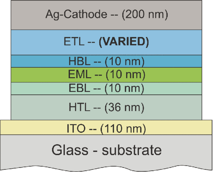 In order to provide reliable data for this study, the layer thicknesses of the diodes were checked using optical simulations. The complete series was produced on one substrate using a common mask for all the layers except the ETL. For the deposition of the ETL, different shadow masks were used to fabricate different ETL thickness only on several devices on the substrate. With this method, the thickness of the whole stack needs to be checked only once and, for all further devices, only the ETL needs to be changed in the simulations. For each diode, the spectrum of the emission in the 0-deg direction (i.e., the direction normal to the OLED substrate) and the spectra at different angles were simulated and the layer thicknesses were varied to fit the measured spectra. Figure 2 depicts the measured EL spectrum at an angle of 0 deg for a device with an ETL thickness of 65 nm. In order to enable for accurate simulation, the complex refractive indices as a function of wavelength were determined by means of reflection-transmission spectroscopy of single supported films for all materials used.10 The current density–voltage ( j–V ) characteristic of the OLEDs was also characterized, showing no significant difference between the devices with varying ETL thicknesses. This can be attributed to appropriate n-doping,9 yielding the possibility to neglect influences such as carrier injection or transport properties. Thus, only optical effects need to be considered in this study. Fig. 2Measured (black) and simulated (red) 0-deg emission spectrum of the device with an ETL thickness of 65 nm showing the good agreement between measurement and simulation. 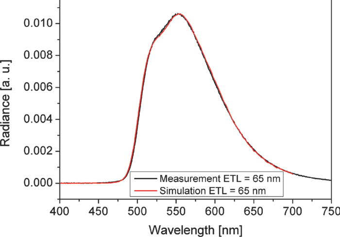 The setup for the time-resolved PL measurements was based on a Nd:YAG Laser (Ekspla PL2210) with a wavelength of 355 nm. The samples were excited under an angle of 20 deg to the surface normal. The pulse length was 30 ps with energy of 10 μJ per pulse. The measurement was performed with a repetition rate of 50 Hz. The time-dependent PL decay was recorded normal to the surface with a streak-camera system (Hamamatsu C5680). The EL measurements were performed in an integrating sphere, which was connected to a source-measurement unit (Keithley 2400) and a fiber spectrometer (Instrument Systems CAS 140). Prior to the measurement a calibration with a halogen lamp was performed with and without the device in order to correct for OLED self-absorption. The substrate edges were blackened in order to avoid an influence from side emission. The Keithley 2400 and the CAS 140 spectrometer were also used for the measurement of the emission spectra. 3.TheoryNear-field phenomena and the photonic mode density must be considered when computing the optical behavior of emissive sites inside the thin-film structure formed by the layers of an OLED. The algorithm used to perform the optical calculations in this study is based on an early work of Sommerfeld,11 who investigated the propagation of radiowaves due to dipole antennas above the Earth's surface by means of a Hertz-Vector representation. Later, this model was adapted by Chance12 [Chance, Prock, and Silbey (CPS)] for molecular fluorescence and energy transfer near interfaces. This rigorous approach uses dyadic Green's functions to describe effects classically. Danz13 extended the CPS model to the general case of arbitrary multilayer systems. According to CPS,12 the electric field [TeX:] $\vec E(\vec r)\exp \left( { - i\omega t} \right)$ due a harmonic oscillating current distribution [TeX:] $\vec j(\vec r)\exp \left( { - i\omega t} \right)$ in a thin-film system can be calculated by the use of the following Green's function G = G0 + S: [TeX:] \documentclass[12pt]{minimal}\begin{document}\begin{equation}
\vec E(\vec r) = i\omega \mu _0 \int {{\rm G}(\vec r,\vec r'} )\vec j(\vec r'){\rm d}^3 \vec r',
\end{equation}\end{document}
where μ0 is the free-space permeability, ω is the angular light frequency, and [TeX:] $t,\vec r$
denote time and space coordinates. Here, the total Green's function is decomposed into the Green's function G0 of the homogeneous emitter medium and a scattering contribution GS due to the multilayer system. The decay rate b (inverse lifetime) of a dipole emitter at the position [TeX:] $\vec r_0^{}$
with a dipole moment [TeX:] $\vec p$
inside a cavity can be derived from the rate of energy dissipation and is calculated using [TeX:] \documentclass[12pt]{minimal}\begin{document}\begin{equation}
\frac{b}{{b_0 }} = 1 + q\frac{{{\mathop{\rm Im}\nolimits} [\vec p{\rm G}_{\rm S} (r_0 ,r_0 )\vec p]}}{{{\mathop{\rm Im}\nolimits} [\vec p{\rm G}_{\rm 0} (r_0 ,r_0 )\vec p]}},
\end{equation}\end{document}
where q is the internal luminescence quantum efficiency and b0 is the decay rate of the infinite emitter medium. A more detailed analysis is given by Danz,13 and the references therein. In result, the relative change in transition rate of the dipole normalized to the spontaneous emission rate in the infinite emissive medium without boundaries can be calculated. The geometric configuration of the microcavity alters the radiative rate and the spatial distribution of the emitted radiation.9 The emitter cathode distance mainly determines the interference conditions at the position of the emissive sites. Consequently, the external output of an OLED structure (i.e., the light that is not total internally reflected but directed into the escape cone) severely depends on the thickness of the ETL defining the distance of the emission layer to the cathode mirror. The model outlined above allows calculating the extracted power as a function of ETL thickness by integrating the angular emission into the ambient over the entire half sphere.Our method for the determination of qEL is based on the computation of the fraction of light extracted from the device as a function of ETL thickness. Figure 3 depicts the calculated emitted power of the green OLED series as a function of ETL thickness for different values of q assuming a constant emission zone and isotropic emitter orientation distribution. These assumptions were experimentally verified by utilizing approaches presented elsewhere.14 Figure 3 shows the absolute emitted power calculated for four different q values. The emitted power strongly depends on the distance to the cathode mirror leading to two maxima at ETL thicknesses of about 60 and 200 nm for this green OLED series. Fig. 3Plot of the integral emission into air as a function of the ETL thickness for different assumptions of the internal luminescence quantum efficiency: (a) absolute values and (b) normalized to the value of the first maximum. 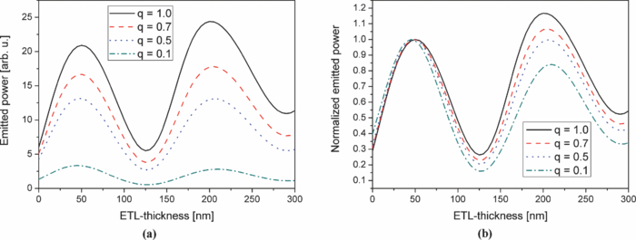 In Fig. 3, the calculated emitted power for the different q values were normalized to their first maximum. It can be seen that the value of q alters the shape of the power plot as a function of ETL thickness and is not acting as a multiplicative factor only [see Eq. 1]. For high q values (i.e., q > 0.5), the second maximum is higher than the first maximum, which has been observed before.15 On the contrary, for lower q values, the first maximum is higher. Consequently, the q value corresponding to the specific emitter system must be considered when designing OLEDs with optimum light output. The method for the determination of qPL uses the phosphorescence lifetime measured on the same OLED structures under PL excitation, as will be discussed in detail in Sec. 4. 4.Results and Discussion4.1.PhotoluminescenceTime-resolved measurements of the PL intensity allow for the determination of the phosphorescence lifetime τPL. Figure 4 shows an example of the measured decay time for the device with an ETL thickness of 34 nm, including a monoexponential fit to the long-living tail of the decay signal. The initial deviation from the monoexponential decay can be attributed to bimolecular annihilation processes.16 Here, the PL lifetime τPL is fitted to a value of τPL = 0.47 μs. The fitting was performed for all measured devices, and the results are plotted in Fig. 4. In the following, we describe how qPL (extracted from PL) can be quantified based on the measurement of the lifetime τPL. The measured lifetime is a superposition of the radiative (R) and nonradiative (NR) lifetimes, [TeX:] \documentclass[12pt]{minimal}\begin{document}\begin{equation}
\frac{1}{{\tau _{{\rm PL}} }} = b_{{\rm PL}} = b_{\rm R} + b_{{\rm NR}} .
\end{equation}\end{document}
The radiative lifetime depends not only on the internal luminescence quantum efficiency q of the emitter but also on the geometric configuration of the microcavity.17 By contrast, the nonradiative lifetime is not affected by the optical environment, as assumed for deriving the rate (inverse lifetime) relation given in Eq. 3. Recalling the definition of q, [TeX:] \documentclass[12pt]{minimal}\begin{document}\begin{equation}
q = \frac{{b_{\rm R} }}{{b_{\rm R} + b_{{\rm NR}} }}.\vspace*{-6pt}
\end{equation}\end{document}
points out that changes of the radiative lifetime correspond to changes in the resulting q value.Fig. 4(a) Measured (black) phosphorescence intensity after short-pulse PL excitation for the device with an ETL thickness of 34 nm. Best monoexponential fit for the long-living tail of the decay signal (red) yields a PL lifetime of 0.47 μs. (b) Fitted phosphorescence lifetimes for all devices under study as a function of ETL-thickness. The huge error bars at 126 and 284 nm ETL thickness originate from the weak PL signals due to emitter position in outcoupling minima to air (see Fig. 7). 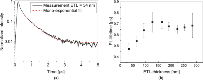 In Fig. 5, the resulting normalized PL lifetimes τPL obtained from these calculations are plotted as a function of ETL thickness for the different q values from 0.1 to 1 (solid lines). According to our simulations, the free-space lifetime yields τ0 = 0.69 μs. This allows fitting Eq. 3 to the measurement data. The measured values of the phosphorescence lifetime τPL (black squares) have also been normalized on τ0. The data are plotted in Fig. 5. Fig. 5Black squares: measured PL lifetime as a function of ETL thickness. Solid lines: simulated change in PL lifetime as a function of ETL thickness. All values are normalized to the free-space PL lifetime τ0 = 0.69 μs. 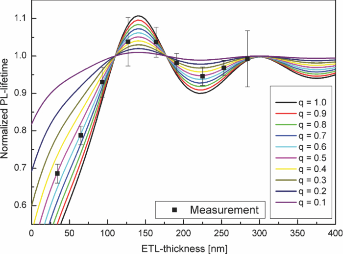 It can be clearly seen that the change of the PL lifetime depends on both the thickness of the ETL and the value of the internal luminescence quantum efficiency q, especially close to the mirror. For very thin ETL layers, the internal luminescence quantum efficiency strongly affects the lifetime because of strong coupling into surface plasmon polaritons8 close to the metal cathode. The comparison of measurement and simulation leads to a value of qPL = 0.5 ± 0.1. Hence, only half of the excitons generated by optical excitation are transferred into radiation, while the other half is lost by nonradiative transitions. 4.2.ElectroluminescenceThe determination of the internal luminescence quantum efficiency qEL under electrical operation is also based on a comparison of measured values with simulation results. Here the measurements are performed in an integrating sphere operating the OLEDs under different current densities. The measurements were performed in two modes: First, the OLEDs are measured without an outcoupling structure and, in a second measurement, with a half-ball lens optically coupled to the substrate surface. The lens has a 25-mm diameter and a refractive index of n = 1.52, matching the substrate refractive index exactly. Thus, the light that is trapped inside the substrate can be coupled out when applying the half-ball lens atop the device. The advantage of these two measurements is a good control, because both measurements have to yield to consistent results for qEL. In Fig. 6, the optical output power obtained from measurements with the half-ball lens at a current density of j = 1.0 mA/cm2 is plotted (right axis). Additionally, the corresponding results from the simulation of the light output into the substrate are given in the same graph. In the simulations, q has been varied between 0.2 and 1.0, allowing the extraction of qEL by comparing the measurement to the simulation. Both experimental and simulation data have been normalized to the light output of the device with 126-nm ETL thickness (right axis). This representation of the data allows comparing the curve progression of both data sets. Fig. 6Black squares: integrating sphere measurements of total emitted power with optically coupled half-ball lens. Lines: simulated emitted power as a function of ETL thickness for different values of the internal luminescence quantum efficiency q. The simulation data are normalized to an ETL thickness of 126 nm. 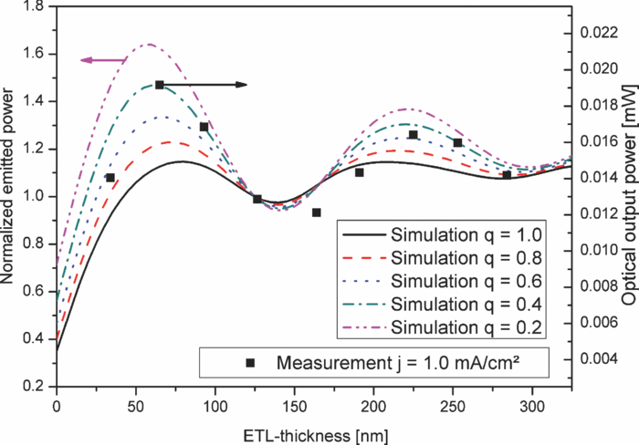 It can be seen that the results from the measurement follow the predicted variation in emitted power obtained from the simulations. Also in the case of electrical driven measurements, the curve progression of the power plot as a function of ETL thickness depends on the value of q. According to Fig. 6, the simulation assuming qEL = 0.4 reproduces the experimental data well. Moreover, the assumption of an internal luminescence efficiency of q = 1, often associated with phosphorescent emissive materials, will lead to wrong OLED efficiency predictions. Furthermore, the dependency of qEL on the current density can be investigated by performing these measurements at different current densities. In our devices, appropriate blocking materials are used and a charge balance factor of γ = 1 can be assumed [see Eq. 1]. When the measured quantum efficiency is brought into correlation with optical power data (obtained from the simulation), one should keep in mind that the outcoupled spectra depend on the ETL thickness, leading to ETL-dependent nonlinearity between EQE and power efficiency. By analyzing our measurement data, we have found a deviation of <4% between the values of the EQE and the corresponding values of power contribution of the green-emitting devices. In Fig. 7, the results for measurements at current densities from 0.1 to 1000 mA/cm2 with and without the half-ball lens as a function of ETL thickness are shown and compared to the simulation results. Fig. 7Measured EQE (dots) and simulated (lines) power contribution as a function of the ETL thickness for the measurement in an integrating sphere (a) with and (b) without the optically coupled half-ball lens. 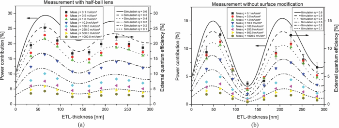 The decrease of the EQE with increasing current density can clearly be seen. In Fig. 7, the measurements and simulations with the half-ball lens are shown. In this case, the first maximum is always higher than the second. Consequently, the emissive sites should be placed in the first maximum when an outcoupling structure is used. This is in contrast to the measurements shown in Fig. 7. It can be seen that for q = 0.6 (and higher values, not shown in the graph), the second maximum is higher than the first one. Thus, if the efficiency of the emitter could be more than q = 0.5, then the emitter should be placed in the second maximum. In both cases, the comparison of the measurements to the simulation leads to the same value of the current dependent internal luminescence quantum efficiency. From these measurements, the current dependency of qEL can be extracted and is depicted in Fig. 8. Fig. 8Determined internal luminescence quantum efficiency of the green emitter as a function of current density. 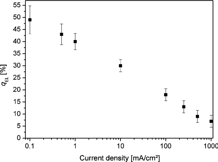 From the PL measurements, a value of qPL = 0.5 ± 0.1 was determined. For the electrical driven devices, this value is only reached for very low current densities. With increasing current density, the difference between qEL and qPL increases. One reason for this difference is the missing current flow during the PL measurements. Because the host of the dye is predominantly electron conductive, the generated excitons will mainly be located at the interface between the emitter and the EBL.18 This leads to a relatively narrow emission zone. In PL measurements, excitons are generated in the whole emitting layer and can recombine in the whole layer. This leads to lower exciton densities associated with weaker exciton quenching.19 With increasing current density, the difference between qPL and qEL increases strongly. This is expected because with increasing current density the rate of competing nonradiative processes, such as triplet-triplet or triplet-polaron, annihilation increases.20, 21 Especially at very high current density, the effect of Joule heating leads to significant singlet-heat annihilation and exciton dissocitation that can no longer be neglected.22 The knowledge of the current dependency of qEL is a very important fact for the design of the devices. The assumption of 100% internal luminescence quantum efficiency will lead to wrong simulation predictions, and also, the distance to the cathode has to be adapted to the desired current density. The internal luminescence quantum efficiency of the green emitter considered in the present study is about q = 0.5 for lower current densities. According to the simulation results (Fig. 3) and to our measurements of the devices with 65 and 225 nm ETL at low current densities, these two ETL thickness values will lead to devices of the same efficiency: From the plots in Figs. 3 and 7, it can be seen that for a q value of 0.5, the first and second maximum are at the same height. However, increasing the current densities the first maximum will lead to a higher efficiency because qEL is reduced to <0.5 due to triplet-triplet or triplet-polaron annihilation. On the other hand, for an emitter with q > 0.5, it will be more favorable to place it in the second maximum—provided that qEL is not significantly reduced by competing nonradiative processes. This is especially important for the design of high-brightness OLEDs, which are driven at higher current densities, resulting in a lower internal luminescence quantum efficiency under operation. 5.ConclusionIn conclusion, we have discussed two different methods to determine the internal luminescence quantum efficiency q of OLED emissive materials. The PL-measurement-based method allows one to get a rough estimation of the q value without the need to fabricate complete OLEDs. This is important for a rapid characterization of new emitter materials. The EL-based method enables for determining the internal luminescence quantum efficiency at different current densities. This is of great importance if OLEDs are designed for significantly higher or lower brightness levels. Consequently, the assumption of efficiency close to unity often used can lead to wrong efficiency predictions and layer thicknesses. At least a rough quantification of q from the PL-based measurements should be performed before designing OLEDs. In this study, the internal luminescence quantum efficiency of the emitter used is only half the value of the theoretical maximum of q = 1.0. Thus, the determination of the internal luminescence quantum efficiency gives the material and device developers feedback about the potential for further improvement of the emitter systems. AcknowledgmentsThe authors thank the Deutsche Forschungsgemeinschaft (DFG) and the German Federal Ministry of Education and Research (BMBF) for funding part of this work under Contract No. FKZ 13N10474 (TOPAS 2012). ReferencesT. Nakamura, N. Tsutsumi, N. Juni, and H. Fujii,
“Improvement of coupling-out efficiency in organic electroluminescent devices by addition of a diffusive layer,”
J. Appl. Phys., 96
(11), 6016
–6022
(2004). http://dx.doi.org/10.1063/1.1810196 Google Scholar
S. Möller and S. R. Forrest,
“Improved light out-coupling in organic light emitting diodes employing ordered microlens arrays,”
J. Appl. Phys., 91
(5), 3324
–3327
(2002). http://dx.doi.org/10.1063/1.1435422 Google Scholar
J. J. Shiang, T. J. Faircloth, and A. R. Duggal,
“Experimental demonstration of increased organic light emitting device output via volumetric light scattering,”
J. Appl. Phys., 95
(5), 2889
–2895
(2004). http://dx.doi.org/10.1063/1.1644038 Google Scholar
T. Tsutsui, E. Aminaka, C. P. Lin, and D.-U. Kim,
“Extended molecular design concept of molecular materials for electroluminescence: sublimed-dye films, molecularly doped polymers and polymers with chromophores,”
Phil. Trans. R. Soc. Lond. A, 355 801
–813
(1997). http://dx.doi.org/10.1098/rsta.1997.0045 Google Scholar
M. A. Baldo, D. F. O'Brien, Y. You, A. Shoustikov, S. Sibley, M. E. Thompson, and S. R. Forrest,
“Highly efficient phosphorescent emission from organic electroluminescent devices,”
Nature, 395 151
–154
(1998). http://dx.doi.org/10.1038/25954 Google Scholar
S. Nowy, B. C. Krummacher, J. Frischeisen, N. A. Reinke, and W. Brütting,
“Light Extraction and optical loss mechanisms in organic light-emitting diodes: influence of the emitter quantum efficiency,”
J. Appl. Phys., 104
(12), 123109
(2008). http://dx.doi.org/10.1063/1.3043800 Google Scholar
L. H. Smith, J. A. E. Wasey, I. D. W. Samuel, and W. L. Barnes,
“Light out-coupling efficiencies of organic light-emitting diode structures and the effect of photoluminescence quantum yield,”
Adv. Func. Mat., 15 1839
–1844
(2005). http://dx.doi.org/10.1002/adfm.200500283 Google Scholar
M. Flämmich, M. C. Gather, N. Danz, D. Michaelis, and K. Meerholz,
“In-situ measurement of the internal luminescence qunatum efficiency in organic light-emitting diodes,”
Appl. Phys. Lett., 95
(26), 263306
(2009). http://dx.doi.org/10.1063/1.3279144 Google Scholar
B. C. Krummacher, S. Nowy, J. Frischeisen, M. Klein, and W. Brütting,
“Efficiency analysis of organic light-emitting diodes based on optical simulation,”
Organ. Electron., 10 478
–485
(2009). http://dx.doi.org/10.1016/j.orgel.2009.02.002 Google Scholar
M. Flämmich, N. Danz, D. Michaelis, A. Bräuer, M. C. Gather, J. H.-W. M Kremer, and K. Meerholz,
“Dispersion-model-free determination of optical constants: application to materials for organic thin film devices,”
Appl. Opt., 48
(8), 1507
–1513
(2009). http://dx.doi.org/10.1364/AO.48.001507 Google Scholar
A. Sommerfeld,
“Über die Ausbreitung der Wellen in der drahtlosen Telegraphie,”
Ann. Phys., 333
(4), 665
–736
(1909). http://dx.doi.org/10.1002/andp.19093330402 Google Scholar
R. R. Chance, A. Prock, and R. Silbey,
“Molecular fluorescence and energy transfer near interfaces,”
Adv. Chem. Phys., 37 1
–65
(1978). http://dx.doi.org/10.1002/9780470142561.ch1 Google Scholar
N. Danz, R. Waldhäusl, and A. Bräuer,
“Dipole lifetime in stratified media,”
J. Opt. Soc. Am. B., 19
(3), 412
–419
(2002). http://dx.doi.org/10.1364/JOSAB.19.000412 Google Scholar
M. Flämmich, M. C. Gather, N. Danz, D. Michaelis, A. H. Bräuer, K. Meerholz, and A. Tünnermann,
“Orientation of dipoles in OLEDs: quantitative in situ analysis,”
Organ. Electron., 11 1039
–1046
(2010). http://dx.doi.org/10.1016/j.orgel.2010.03.002 Google Scholar
C.-L. Lin, T.-Y. Cho, C.-H. Chang, and C.-C. Wu,
“Enhancing light outcoupling of organic light-emitting diodes by locating emitters around the second antinode of the reflective metal electrode,”
Appl. Phys. Lett., 88
(8), 081114
(2006). http://dx.doi.org/10.1063/1.2178485 Google Scholar
M. A. Baldo, C. Adachi, and S. R. Forrest,
“Transient analysis of organic electrophosphorescence. II. transient analysis of triplet-triplet annihilation,”
Phys. Rev. B, 62
(16), 10967
(2000). http://dx.doi.org/10.1103/PhysRevB.62.10967 Google Scholar
S. Mladenovski, S. Reineke, and K. Neyts,
“Measurement and simulation of exciton decay times in organic light-emitting devices with different layer structures,”
Opt. Lett., 34
(9), 1375
–1377
(2009). http://dx.doi.org/10.1364/OL.34.001375 Google Scholar
F. So, B. Krummacher, M. K. Mathai, D. Poplavskyy, S. A. Choulis, and V.-E. Choong,
“Recent progress in solution processable organic light emitting devices,”
J. Appl. Phys., 102
(9), 091101
(2007). http://dx.doi.org/10.1063/1.2804122 Google Scholar
S. Reineke, K. Walzer, and K. Leo,
“Triplet-exciton quenching in organic phosphorescent light-emitting diodes with Ir-based emitters,”
Phys. Rev. B, 75
(12), 125328
(2007). http://dx.doi.org/10.1103/PhysRevB.75.125328 Google Scholar
N. C. Giebink and S. R. Forrest,
“Quantum efficiency roll-off at high brightness in fluorescent and phosphorescent organic light emitting diodes,”
Phys. Rev. B, 77
(23), 235215
(2008). http://dx.doi.org/10.1103/PhysRevB.77.235215 Google Scholar
J. Kalinowski, M. Cocchi, V. Fattori, L. Murphy, and J. A. G. Williams,
“Unified approach to electroluminescence efficiency in organic light-emitting diodes,”
Organ. Electron., 11 724
–730
(2010). http://dx.doi.org/10.1016/j.orgel.2010.01.011 Google Scholar
H. Nakanotani, H. Sasabe, and C. Adachi,
“Singlet-singlet and singlet-heat annihilations in fluorescence-based organic light-emitting diodes under steady-state high current density,”
Appl. Phys. Lett., 86
(21), 213506
(2005). http://dx.doi.org/10.1063/1.1939075 Google Scholar
BiographyDaniel S. Setz studied electrical engineering at the University of Ulm, Germany, and received his diploma in 2008. He is working toward his PhD at OSRAM Opto Semiconductors GmbH in Regensburg, Germany, supervised by Professor Albrecht Winnacker (University of Erlangen-Nuremberg, Germany). The focus of his research is the improvement of light extraction and internal efficiency analysis of organic LEDs. Tobias D. Schmidt is a PhD student at the University of Augsburg, Germany. He received his degree for teaching physics and mathematics in 2008. His current research interests are degradation processes and the exciton lifetime in organic LEDs. Michael Flämmich is a PhD student at Abbe School of Photonics at Friedrich-Schiller-University Jena, where he received his diploma in physics in 2007. Currently, he is with the Fraunhofer Institute of Applied Optics and Precision Engineering IOF in Jena, where he focuses on the optical characterization of OLED emissive materials. He has had several research articles published that provide methods to determine the emission zone, dipole orientation, and internal luminescence quantum efficiency for profound optical analyses and optimization of OLEDs. Stefan Nowy studied physics from 2000 to 2005 at the Technical University of Munich, Germany, and received his diploma in 2005. In 2006, he joined Prof. Brütting's OLED group at the University of Augsburg, Germany, as a PhD student, receiving his PhD in 2010. He is now with the Physikalisch-Technische Bundesanstalt in Braunschweig, Germany. Jörg Frischeisen studied physics at the University of Regensburg, Germany, including one year of studies in Boulder, Colorado. He received his diploma in 2006. Subsequently, he started working toward his PhD at the Institute of Physics at the University of Augsburg. He obtained a scholarship from the Elite Network of Bavaria in the framework of the International Graduate School of Materials Science of Complex Interfaces. His main field of research covers organic LEDs with a focus on light extraction and the role of surface plasmon polaritons and waveguide modes in OLEDs, as well as the influence of molecular orientation in doped organic thin films. Benjamin C. Krummacher joined OSRAM Opto Semiconductors in San Jose, California, in 2004, as PhD student in the OLED material and devices team directed by Franky So. His research activities were supervised by Prof. Albrecht Winnacker from the University of Erlangen, Bavaria. The focus of his work was the generation of white light by luminescence conversion of blue OLED-emission and light-extraction improvement. Since 2007, he has been development engineer at the OSRAM OLED R&D center in Regensburg and, currently, he is project leader in the OLED-Lighting Product Development Department. Dr. Krummacher has authored 10 refereed journal papers and created numerous patented inventions in his field. Thomas Dobbertin is heading the technology development for OLED Lighting at OSRAM Opto Semiconductors in Regensburg. He received his diploma in electrical engineering and his PhD in 2001 and 2005, respectively, both from the Technical University of Braunschweig, Germany. His studies covered device-related phenomena in organic optoelectronics with a dedicated focus on OLED stack design. He has been with OSRAM Opto Semiconductors since 2005. Karsten Heuser earned his PhD at the University of Augsburg in solid state physics. In 1999, he joined Siemens Corporate Technology in Erlangen to develop organic LEDs for display applications. In 2005, he joined OSRAM Opto Semiconductors to build up a development center for OLED Lighting. Today, he heads the OLED activities within OSRAM from technology toward lighting applications. Dirk Michaelis received his diploma and PhD in physics in 1994 and 1999, respectively, from the Friedrich-Schiller-University Jena. From 1999 to 2002, he was scientific assistant at the Friedrich-Schiller-University Jena. During that time, he worked in the field of nonlinear optics and dynamical systems. Since 2002, Dr. Michaelis has been with the Fraunhofer Institute of Applied Optics and Precision Engineering (IOF), Jena. At the Fraunhofer Institute, he works in the field of optical design. He is particularly interested in diffractive optics, nonimaging optics, and OLED optics. Norbert Danz received his diploma and PhD in physics from the Friedrich-Schiller-University Jena, Germany, in 1998 and 2003, respectively. Since 1998, he has been with the Fraunhofer-Institute for Applied Optics and Precision Engineering IOF in Jena. His major interests include optical biosensors based on surface plasmon resonance as well as fluorescence effects in inhomogeneous environments (e.g., in the field of OLED optics). Wolfgang Brütting received his PhD in physics from the University of Bayreuth, Bayreuth, Germany, in 1995, with a study on charge transport in 1-D charge-density wave systems. He then moved to the field of organic semiconductors, where he was involved in the development of organic LEDs for display applications. Since 2003, he has been a professor of experimental physics at the University of Augsburg, Augsburg, Germany. His research interests include physics of organic semiconductors, in particular, thin-film growth, photophysics, and electrical transport of these materials and related electronic devices. Albrecht Winnacker received his PhD from the University of Heidelberg, Germany, dealing with optical pumping of color centers. From 1970 to 1972, he was a postdoctoral researcher at the University of California in Berkeley, and in 1972, he joined the University of Heidelberg, where he became professor for experimental physics in 1980. From 1986 to 1991, he was with the Siemens AG, Corporate Technology in Erlangen, Germany, heading a group working on compound semiconductors and phosphors. Since 1991, he has been with the Friedrich-Alexander-University of Erlangen-Nuremberg, Germany, heading the department Materials for Electronics and Energy Technology until receiving emeritus status in 2009. Since 2006, he has been an honorary professor at the Faculty for Physics and Astronomy, University of Heidelberg. Prof. Winnacker has published more than 240 papers in the fields of semiconductors, crystal growth, phosphors, and organic LEDs. |


