|
|
1.IntroductionOver the past few years silicon photonics has experienced tremendous growth.1, 2 , 3, 4 The main reason is compatibility with CMOS technology, which allows one to use existing semiconductor fabrication techniques and provides fabrication of low-cost optoelectronic devices. Significant progress has been made in the fabrication of passive silicon-based devices such as modulators,5 photodetectors,6 and interconnects,7 but still it is difficult to achieve lasing in silicon because of its indirect bandgap. Different approaches to fabricate silicon lasers have been demonstrated, including nanocrystalline silicon structures,8 Si/Ge quantum cascade structures,9, 10 , 11 and Raman lasers,12 but the resulting efficiencies are very low. For example, the efficiency of a silicon nanocrystal-based LED is 0.1% (Ref. 13) and the efficiency of a Raman silicon laser is 8.5% (Ref. 12). The most successful approach to considerably increase silicon laser efficiency is the hybrid integration of a III–V quantum-well heterostructure with a silicon waveguide.14, 15, 16, 17, 18 This type of laser is called a hybrid silicon evanescent laser (SEL). Thus, differential quantum efficiencies of optical pumped and electrical pumped SELs are 15% (Ref. 19) and 46% (Ref. 15), respectively. A great deal of experimental data can be found in the literature concerning SELs, but there is still a need for theoretical research in this area. A numerical self-consistent dynamic model of electrically pumped hybrid silicon evanescent lasers is presented in this work. 2.Numerical SimulationA cross section of an electrically pumped SEL is schematically shown in Fig. 1 (Ref. 15). The laser consists of two regions: a silicon-on-insulator (SOI) passive rib waveguide and a InGaAlAs/InP active region that provides optical gain. The SOI waveguide width w is 2.5 μm, height h is 0.69 μm, and rib etch depth d is 0.52 μm. The active region is based on AlGaInAs quantum wells with photoluminescence peaks at 1303 nm. Optical radiation propagates mainly through the silicon waveguide. Laser gain in such a structure is achieved due to the silicon waveguide optical mode overlapping with an active layer. We have developed a numerical self-consistent dynamic model of the SEL based on these assumptions: quasi-stationary approximation, uniform distribution of light intensity and carrier concentration in the z-y plane, and neglected carrier diffusion. Carrier concentration and photon density dynamics in the resonator are described by coupled rate equations (for example, see Ref. 20). On the assumptions mentioned above, these equations take on the form [TeX:] \documentclass[12pt]{minimal}\begin{document}\begin{equation}
\frac{{dN(t)}}{{dt}} = \frac{J}{{ed}} - \frac{{N(t)}}{{\tau _{{\rm sp}} }} - \sum\limits_{i = 1}^m {\tilde \Gamma _i } G_i (t)S_i (t),
\end{equation}\end{document}
[TeX:] \documentclass[12pt]{minimal}\begin{document}\begin{equation}
\frac{{dS_1 (t)}}{{dt}} = \tilde \Gamma _1 \Gamma G_1 (t)S_1 (t) - \frac{{S_1 (t)}}{{\tau _{\rm p} }} + \Gamma \beta \frac{{N(t)}}{{\tau _{{\rm sp}} }},
\end{equation}\end{document}
[TeX:] \documentclass[12pt]{minimal}\begin{document}\begin{equation}
\frac{{dS_m (t)}}{{dt}} = \tilde \Gamma _m \Gamma G_m (t)S_m (t) - \frac{{S_m (t)}}{{\tau _{\rm p} }} + \Gamma \beta \frac{{N(t)}}{{\tau _{{\rm sp}} }},
\end{equation}\end{document}
where Si(t) is the resonator volume-averaged i’th optical mode photon density, N(t) is the active layer volume-averaged carrier concentration, J is the pump current density, e is the electron charge, d is the active layer thickness, τsp is the carrier spontaneous recombination time, τp is the photon lifetime in the resonator, β is the spontaneous recombination coefficient (fraction of spontaneous radiation that is amplified), Gi(t) is the i’th mode optical gain, Γ and [TeX:] $\tilde \Gamma _i$
are optical confinement factors, and m is the number of transversal optical modes that are taken into account.The first equation states that the speed of carrier concentration variations depends on spontaneous and stimulated recombination rates and electrical pumping. Second and subsequent equations state that photon density variation speed depends on photon production rate, spontaneous recombination rate, and photon losses in the resonator. Intensity evolution of the i’th optical mode can be described in terms of gain coefficients Gi(t), which can be calculated as: [TeX:] \documentclass[12pt]{minimal}\begin{document}\begin{equation}
G_i (t) = - 2\,{\mathop{\rm Im}\nolimits} \,\omega _i (t),
\end{equation}\end{document}
where Im represents the imaginary part of a complex number.These gain coefficients are time dependent, because the i’th optical mode complex frequency ωi (complex eigenvalue of wave equation) varies with time. To obtain Gi(t), resonant frequencies ωi are calculated in the first stage from resonator parameters by solving a scalar wave equation. Then, gain coefficients are used to calculate carrier concentrations at the next time step from Eqs. 1, 2, 3, 4. Carrier concentration variations lead to active layer refractive index variation; thus, it is necessary to recalculate resonant frequencies at which laser generation occurs and optical modes gain coefficients at every time step in a finite-difference algorithm. Total computational time directly depends on the time required for resonant frequency calculation. To decrease this time and enhance computational efficiency of the algorithm, we used a special computational technique that was proposed earlier in Ref. 21. 3.Results and DiscussionTwo lower order optical mode profiles calculated at the beginning of the simulation are shown in Fig. 2. Spatial intensity distribution was calculated at every time step during the simulation, with resonator optical property variations taken into account. The confinement factor, defined as the ratio of the average value of electromagnetic field intensity in the active region to its average value in the resonator, was calculated for each optical mode: [TeX:] \documentclass[12pt]{minimal}\begin{document}\begin{equation*}
\hspace*{94pt}\tilde \Gamma _i = \frac{{\int_{V_{{\rm act}} } {\left| {\psi _i (x)} \right|} ^2 dV/V_{{\rm act}} }}{{\int_{V_{{\rm cav}} } {\left| {\psi _i (x)} \right|} ^2 dV/V_{{\rm cav}} }},
\end{equation*}\end{document}
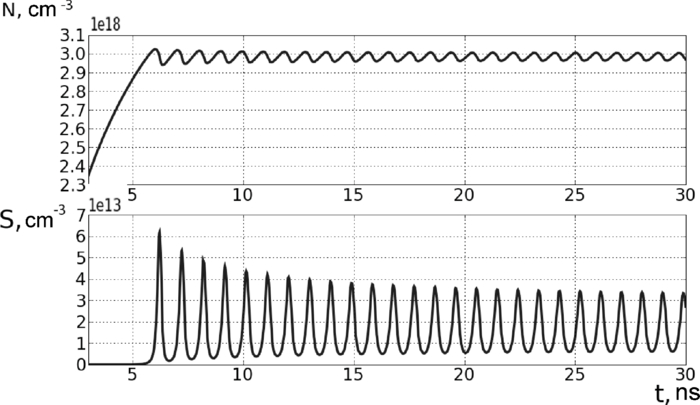
where ψi(x) is the i’th optical mode profile, Vact is the active region volume, and Vcav is the cavity volume. Confinement factor Γ is defined as the ration of the active region volume to the volume of the whole resonator: Γ = Vact/Vcav.Fig. 2Hybrid laser structure optical mode profiles: (a) TE0 and (b) TE0, where |ψ| is the magnitude of the normalized nonzero electrical field component and n is the profile of the real part of the refractive index. 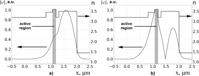 The proposed algorithm was used to determine laser structure mode composition. As follows from Fig. 2, the first-order mode overlapping with an active region is considerably higher than that for the fundamental mode. Therefore, laser generation is expected only for the first-order mode. This result is confirmed by experimental data.15 Thus, spatial separation between the active region and silicon waveguide leads to laser single-mode operation. Output radiation intensity as a function of time for a given pump current value was calculated. After the transient processes finished, output radiation power could be evaluated. Implementation of this procedure to several pump current values allows us to obtain laser P–I characteristics. These characteristics and corresponding experimental data15 are shown in Fig. 3. Approximations for linear sections of P–I characteristics are also presented. Calculated values of threshold current and curve slope—31 mA and 0.57 W/A, correspondingly—are in good agreement with experimental data of a threshold pump current of 29 mA and linear section slope of 0.42 W/A. Fig. 3SEL's output power P as a function of drive current I. Experimental data (Ref. 15) and obtained numerical results are presented. 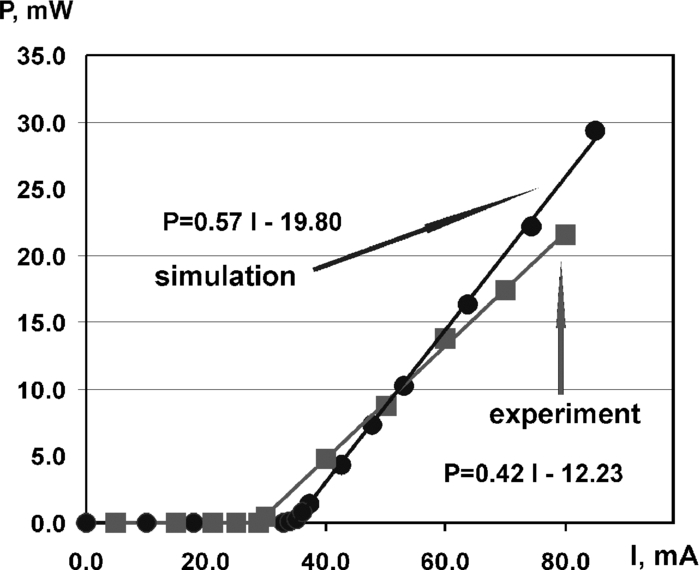 Dynamic properties of SELs were also investigated. It was shown that the laser current-step response is the typical inversion population and photon density relaxation oscillation process. When the pump current reaches some critical value, the laser response takes the form of periodical self-sustained pulses. An example of such a self-modulation process at 1.22 times the threshold pump current is shown in Fig. 4. The oscillation frequency is ~1 GHz. Self-modulation in SELs is of great interest because it provides a higher signal-to-noise ratio in optical communication and optical storage read-write systems. 4.ConclusionA self-consisted dynamic model of a silicon evanescent laser based on the numerical solution of a scalar wave equation and coupled rate equations is developed. In order to enhance the computational efficiency of the proposed method, a special technique for resonant frequency calculation from the resonator parameters is utilized. The SEL's output power as a function of drive current and its mode composition are obtained. These results are in good agreement with published experimental data. The proposed model also allows us to investigate dynamic processes in hybrid lasers. It is shown that the SEL's current-step response is the typical inversion population and photon density relaxation oscillation process. Under certain conditions, periodical self-sustained pulses are observed. ReferencesB. Jalali, M. Paniccia, and G. Reed,
“Silicon photonics.,”
IEEE Microwave Mag., 7 58
–68
(2006). http://dx.doi.org/10.1109/MMW.2006.1638290 Google Scholar
L. Tsybeskov, D. J. Lockwood, and M. Ichikawa,
“Silicon photonics: CMOS going optical,”
Proc. IEEE, 97 1161
–1165
(2009). http://dx.doi.org/10.1109/JPROC.2009.2021052 Google Scholar
R. A. Soref,
“Silicon-based optoelectronics,”
Proc. IEEE, 81 1687
–1706
(1993). http://dx.doi.org/10.1109/5.248958 Google Scholar
O. Bisi, S. U. Campisano, L. Pavesi, and F. Priolo, Silicon Based Micro-Photonics: From Basics to Applications, 279 IOS Press, Amsterdam
(1999). Google Scholar
D. Marris-Morini, L. Vivien, G. Rasigade, J.-M. Fedeli, E. Cassan, X. L. Roux, P. Crozat, S. Maine, A. Lupu, P. Lyan, P. Rivallin, M. Halbwax, and S. Laval,
“Recent progress in high-speed silicon-based optical modulators,”
Proc. IEEE, 97 1199
–1215
(2009). http://dx.doi.org/10.1109/JPROC.2009.2015337 Google Scholar
L. Vivien, J. Osmond, J.-M. Fedeli, D. Marris-Morini, P. Crozat, J.-F. Damlencourt, E. Cassan, Y. Lecunff, and S. Laval,
“42 GHz p.i.n. germanium photodetector integrated in a silicon-on-insulator waveguide,”
Opt. Express, 17 6252
–6257
(2009). http://dx.doi.org/10.1364/OE.17.006252 Google Scholar
A. Sure, T. Dillon, J. Murakowski, C. C. Lin, D. Pustai, and D. W. Prather,
“Fabrication and characterization of three-dimensional silicon tapers,”
Opt. Express, 11 3555
–3561
(2003). http://dx.doi.org/10.1364/OE.11.003555 Google Scholar
L. T. Canham,
“Silicon quantum wire array fabrication by electrochemical and chemical dissolution of wafers,”
Appl. Phys. Lett., 57 1046
–1048
(1990). http://dx.doi.org/10.1063/1.103561 Google Scholar
R. A. Soref,
“Prospects for novel Si-based optoelectronic devices: unipolar and p-i-p-i lasers,”
Thin Solid Films, 294 325
–329
(1997). http://dx.doi.org/10.1016/S0040-6090(96)09261-9 Google Scholar
G. Dehlinger, L. Diehl, U. Gennser, H. Sigg, J. Faist, K. Ensslin, and D. Grutzmacher,
“Intersubband electroluminescence from silicon-based quantum cascade structures,”
Science, 290 2277
–2280
(2000). http://dx.doi.org/10.1126/science.290.5500.2277 Google Scholar
L. Diehl, S. Mentese, H. Sigg, E. Muller, D. Grutzmacher, U. Gennser, I. Sagnes, T. Fromherz, J. Stangl, T. Roch, G. Bauer, Y. Campidelli, O. Kermarrec, D. Bensahel, and J. Faist,
“Electroluminescence from strain compensated Si0.2Ge0.8/Si quantum-cascade structures based on a bound-to-continuum transition,”
Appl. Phys Lett., 81 4700
–4702
(2002). http://dx.doi.org/10.1063/1.1528729 Google Scholar
O. Boyraz and B. Jalali,
“Demonstration of a silicon Raman laser,”
Opt. Express, 12 5269
–5273
(2003). http://dx.doi.org/10.1364/OPEX.12.005269 Google Scholar
G. Franzò, A. Irrera, E. C. Moreira, M. Miritello, F. Iacona, D. Sanfilippo, G. Di Stefano, P. G. Fallica, and F. Priolo,
“Electroluminescence of silicon nanocrystals in MOS structures,”
Appl. Phys. A, 74 1
–5
(2002). http://dx.doi.org/10.1007/s003390101019 Google Scholar
H. Park, A. W. Fang, S. Kodama, and J. E. Bowers,
“Hybrid silicon evanescent laser fabricated with a silicon waveguide and III–V offset quantum wells,”
Opt. Express, 13 9460
–9464
(2005). http://dx.doi.org/10.1364/OPEX.13.009460 Google Scholar
H.-H. Chang, A. W. Fang, M. N. Sysak, H. Park, R. Jones, O. Cohen, O. Raday, M. J. Paniccia, and J. E. Bowers,
“1310 nm silicon evanescent laser,”
Opt. Express, 15 11466
–11471
(2007). http://dx.doi.org/10.1364/OE.15.011466 Google Scholar
B. R. Koch, A. W. Fang, O. Cohen, and J. E. Bowers,
“Mode-locked silicon evanescent lasers,”
Opt. Express, 15 11225
–11233
(2007). http://dx.doi.org/10.1364/OE.15.011225 Google Scholar
A. W. Fang, E. Lively, Y.-H. Kuo, D. Liang, and J. E. Bowers,
“A distributed feedback silicon evanescent laser,”
Opt. Express, 16 4413
–4419
(2008). http://dx.doi.org/10.1364/OE.16.004413 Google Scholar
A. W. Fang, M. N. Sysak, B. R. Koch, R. Jones, E. Lively, Y.-H. Kuo, D. Liang, O. Raday, and J. E. Bowers,
“Single-wavelength silicon evanescent lasers,”
J. Sel. Top. Quant. Electron., 15 535
–544
(2009). http://dx.doi.org/10.1109/JSTQE.2009.2014251 Google Scholar
A. W. Fang, H. Park, S. Kodama, and J. E. Bowers,
“An optically pumped silicon evanescent laser,”
(2005) Google Scholar
B. Mroziewicz, M. Bugajski, and W. Nakwaski, Physics of Semiconductor Lasers, 366 PWN, Warszawa
(1991). Google Scholar
A. G. Rzhanov and S. E. Grigas,
“Determination of guided modes in multilayer dielectric waveguides,”
Numer. Meth. Program., 10 72
–76
(2009). Google Scholar
BiographyAlexey G. Rzhanov is an assistant professor at the M.V. Lomonosov Moscow State University, where he received his MS in physics in 1984 and PhD in radio physics and quantum electronics in 1994. He is the author of more than 40 journal papers. His current research interests include injection laser and photovoltaic light converters modeling and photonic and optoelectronic systems. Stanislav E. Grigas received his MS in physics from the M.V. Lomonosov Moscow State University in 2010, where he is currently a PhD student. He is the author of two journal papers. His current area of research is the modeling and numerical simulation of optoelectronic devices. His main areas of interest include silicon photonics, semiconductor lasers, and optical waveguides. |