
|
|
1.IntroductionThe continuous drift-diffusion approach in the mean-field (MF) approximation, usually applied in commercially available simulation tools, is often used to model the electric response of metal/insulator/metal (MIM) systems,1 such as organic light-emitting diodes.2, 3, 4 Because insulators are quasi-free of intrinsic charge carriers, carrier supplying contacts are inherently required, serving as source for all carriers entering the insulator and thus determining its conductivity. In order to adequately account for the contact in the overall response of MIM systems, it is therefore of crucial importance to appropriately describe the contact formation between insulator and conductor and the electrical response of such a contact.5 Often, two limits are employed, simplifying the problem. First, the charge-carrier injection is supposed to be strong, leading to an infinite carrier density pi(0) and thus derivative of the electric field strength Fi(0) at the interface in the insulator. Such a boundary condition is used to explain the space-charge limitation of MIM systems, where no influence of the injecting contact on the current voltage (IV) characteristic is observed.6 Second, the carrier supplying contacts are weak. In this case, it is assumed that only few carriers enter the insulator so that their self-induced electric field is always much smaller than the external electric field. As a consequence, the electric field appears to be constant over the entire insulator. This condition is used to model thermionic emission,7, 8 Fowler–Nordheim tunneling,8, 9 or other more suited injection models for an organic semiconductor (OS)10, 11, 12, 13 but fails to describe the equilibrium field and charge-carrier distribution in the MIM system because, in intrinsic insulators, enrichment contacts and, thus, space charge always prevail at zero bias. Apparently, the distinct separation of low and strong injection level does not enable smooth transition between the regimes, which however must be expected. On the one hand, e.g., the depletion of a charge-carrier reservoir provided by the contact should be stimulated by an externally applied voltage as long as the carrier supply by the contact is weak. Thus, eventually a transition from a carrier rich to an injection limited regime can occur. On the other hand, a transition from an injection-limited regime to a space-charge–limited regime can occur once the carrier supply from the contacts disproportionately grow with bias compared to the carrier extraction across the bulk of the insulator. Hence, to describe the IV characteristic of a MIM system over the entire voltage range, no assumptions should be made to fix the boundary conditions. In the first place, the entire MIM system must be comprehensively considered and the boundary conditions should be set far away from the metal/insulator contact in the contact materials itself. There, the contact has no influence on the system condition. In this contribution, the adequate boundary condition at the interface will be first determined, self-consistently, using the drift-diffusion approach in the framework of the MF approximation.5, 14, 15 This already allows for a determination of the electrical response across a wide voltage range in both bias directions, including the transitions between injection-limited and space-charge–limited currents (SCLCs). However, it will be shown that the obtained response of the MIM system on basis of the self-consistent MF boundary conditions is insufficient to describe the IV characteristics appropriately because single-particle (SP) phenomena are not considered.16, 17 On basis of an estimation of the transition criteria between mean-field and SP dominance (SPD), a validity chart will be presented and a modification of the MF boundary conditions will be suggested. 2.Results and Discussion2.1.Mean-Field Drift-Diffusion ApproachFirst consider a single metal/insulator contact, the insulator is semi-infinite in the positive half space in contact with a conductor reaching from 0 to –∞. It is assumed that the conductor can be described in the framework of the linearized Thomas–Fermi approximation. Far away from the conductor/insulator interface, the conductor is not supposed to be influenced by the contact and, thus, the derivative of the electric field vanishes for x → –∞, and the carrier density approaches the equilibrium density. As a consequence, the electric field distribution Fc for the contact material can be derived to be [TeX:] \documentclass[12pt]{minimal}\begin{document}\begin{equation}
F_{\rm c} = \left[ {F_{\rm c} \left( 0 \right) - \frac{j}{{\sigma _{\rm c} }}} \right]\exp \left( {\frac{x}{{l_{{\rm TF}} }}} \right) + \frac{j}{{\sigma _{\rm c} }},
\end{equation}\end{document} where σc is the conductivity of the conductor, lTF is the Thomas–Fermi screening length and j is the current density. The respective electrochemical potential κc reads:
[TeX:] \documentclass[12pt]{minimal}\begin{document}\begin{equation}
\kappa _{\rm c} = el_{{\rm TF}} \left[ {F_{\rm c} \left( x \right) - \frac{j}{{\sigma _{\rm c} }}} \right] + \kappa _\infty + e\phi _{\rm c} + E_{\rm b} ,
\end{equation}\end{document} where Eb is the position of the conduction band bottom, κ∞ the equilibrium value of the chemical potential in the electrode far away from the interface and e is the positive elementary charge.The electric field distribution Fi in the insulator is described by the one dimensional drift-diffusion equation: [TeX:] \documentclass[12pt]{minimal}\begin{document}\begin{equation}
\frac{{k_{\rm B} T}}{e}F''_i - F_i F'_i = - \frac{j}{{\mu _i \varepsilon _i \varepsilon _0 }},
\end{equation}\end{document} where T is the absolute temperature, kB is the Boltzmann constant, μi is the carrier mobility, ɛi is the dielectric constant of the insulator, and ɛ0 is the permittivity of vacuum. Far away from the conductor/insulator interface, the insulator is not supposed to be influenced by the contact and, thus, the derivative of the electric field and the carrier density (wide bandgap material) vanishes for x → +∞. The respective electrochemical potential κi considering Boltzmann statistics reads
[TeX:] \documentclass[12pt]{minimal}\begin{document}\begin{equation}
\kappa _i = E_{\rm b} + \kappa _\infty + \Delta + k_{\rm B} T\ln \left( {\frac{{p_i }}{{N_i }}} \right) + e\phi _i ,
\end{equation}\end{document} where Δ is the injection barrier at the insulator/conductor contact, pi is the carrier density, Ni is the effective density of states, and ϕi is the electrostatic potential in the insulator.The contact formation between insulator and conductor requires, in the first place, the following continuity conditions at the interface to be fulfilled:
Without loss of generality the restrictions to the lack of surface charges and dipole layers can be assumed. Applying these continuity conditions to Eqs. 1, 4, the following boundary condition can be found to solve Eq. 3: [TeX:] \documentclass[12pt]{minimal}\begin{document}\begin{equation}
p_i \left( 0 \right) \approx N_i \exp \left\{ { - \frac{1}{{k_{\rm B} T}}\left[ {\Delta - el_{{\rm TF}} \frac{{\varepsilon _i }}{{\varepsilon _{\rm c} }}F_i \left( 0 \right)} \right]} \right\}.
\end{equation}\end{document} Equation 5 connects the carrier density pi(0) at the interface within the insulator to the prevailing electric field Fi(0). Apparently, an effective injection barrier Δeff = Δ – elTF(ɛi/ɛc)Fi(0) can be defined that contains a field-induced change of the barrier Δ by the voltage drop within a surface near region of thickness lTF in the conductor. Yet, keeping in mind that lTF is on the order of angstroms, an essential contribution of the barrier modification requires rather high electric fields at the interface—respectively, external voltages—to match the expectations.18 Let us assume an injection-limited case where the electric field is constant across the insulator. Then, for an ITO/OS contact with an injection barrier of 0.4 eV, a lTF of 8.6 Å, and ɛi/ɛc = 3/9.3, a reduction of Δ by half would require an electric field on the order of 109 V/m, which would be 100 V for a 100-nm-thick insulator. Be aware that an effective injection barrier of 0.2 eV would yield already severe space-charge effects.14, 18, 19 A transition voltage of 100 V from injection to SCLC with an initial barrier height of only 0.4 eV is, however, an unrealistic high value. 2.2.Single-Particle InfluenceThe discussed problematic stems from an inherent problem of the used one-dimensional mean-field approximation, implying averaging of all variables over the plane perpendicular to the injection current density. However, this procedure is restricted to relatively high carrier densities and does not account for single-particle phenomena, such as the well-known and considered Schottky effect,20, 21 describing the coulombic coupling of a single charge in the insulator to its image in the conductor.8 The superposition of the resulting image charge potential and the external potential yields a modification of the injection barrier, which is given by [TeX:] \documentclass[12pt]{minimal}\begin{document}\begin{equation}
\begin{array}{l}
{{\delta \phi _{{\rm sch}} = \sqrt {\displaystyle\frac{{eF_i \left( 0 \right)}}{{4\pi \varepsilon _i \varepsilon _0 }}} }}\vspace*{6pt}\\
{{x_{\mathop{\rm m}\nolimits} = \sqrt {\displaystyle\frac{e}{{16\pi \varepsilon _i \varepsilon _0 F_i \left( 0 \right)}}} }}
\end{array},
\end{equation}\end{document} where δϕsch is the barrier lowering induced by the Schottky effect, whereas xm denotes the distance of the potential barrier maximum from the physical conductor/insulator contact. Apparently, the barrier lowering due to the Schottky effect is stronger than the aforementioned barrier modification by the field penetration in the contact. Considering again an injection barrier of 0.4 eV and a dielectric constant of the insulator of 3, a reduction of Δ by half would now require an electric field of only 8 × 10⁷ V/m, which would be 8 V for a 100-nm-thick insulator.It is thus essential to estimate the validity region of the MF approximation and the SPD approach. This can be simply done by considering the force on a single carrier in the insulator17 [TeX:] \documentclass[12pt]{minimal}\begin{document}\begin{equation}
f\left( {\vec r} \right) = f_{{\rm ext}} \left( {\vec r} \right) - \frac{{e^2 }}{{16\pi \varepsilon _i \varepsilon _0 x^2 }} - \displaystyle\frac{\partial }{{\partial x}}\int {d^3 r' \cdot } p_i \left( {\vec r'} \right)\displaystyle\frac{{e^2 {\mathop{\rm sgn}} \left( {x'} \right)}}{{4\pi \varepsilon _i \varepsilon _0 \left| {\vec r - \vec r'} \right|}}
\end{equation}\end{document} being composed out of the force from an external field (first term), the force from the coulombic coupling to the individual image charge (second term), and the force from the coulombic coupling to all other charges (last term). It is feasible that the MF approximation is better suited when the interaction with other charges exceeds the one with its own image. On the other hand, the SPD approach should be applied once the coupling to the image charge dominates. Thus, the last term has to be compared to the second term of Eq. 7 at position xm. A rough estimation given in Ref. 17 yields a transition criterion for the validity of the MF and SPD approach,
[TeX:] \documentclass[12pt]{minimal}\begin{document}\begin{equation}
x_{\rm m} \cong 0.2r_i ,
\end{equation}\end{document} expressed in terms of the two characteristic length scales of both approximations: the distance from the Schottky barrier maximum xm to the physical contact and ri = pi(0)−1/3 the average carrier distance in the insulator. The critical field at the contact can thus be extracted from the following transcendental equation:
[TeX:] \documentclass[12pt]{minimal}\begin{document}\begin{equation}
\sqrt {\frac{e}{{16\pi \varepsilon _i \varepsilon _0 F_i \left( 0 \right)}}} = 0.2\left\{ {N_i^{ - 1/3} \exp \left[ {\frac{\Delta }{{3k_{\rm B} T}} - \frac{{eF_i \left( 0 \right)l_{{\rm TF}} }}{{3k_{\rm B} T}}\frac{{\varepsilon _i }}{{\varepsilon _{\rm c} }}} \right]} \right\}.
\end{equation}\end{document} Equation 9 can be solved graphically as depicted in Fig. 1, where the characteristic length xm and 0.2 ri are plotted, exemplarily, in dependence of the electric fields at the interface Fi(0) for typical parameters of ITO and organic semiconductors.22, 23, 24, 25, 26 Apparently, two points of intersection exist and, thus, there are an upper and lower limit for the use of the SPD regime. The dependence of the two corresponding critical fields on the barrier height Δ is depicted in Fig. 2. The SPD approximation is valid in the range of interface fields between Fmin and Fmax, where 0.2·ri > xm. The MF approximation is, on the contrary, below Fmin and above Fmax applicable. Yet, Fmax lies for some fields in a region above the line Flim, above which the applied Boltzmann statistics is violated and hence has no physical meaning. FL marks the field that relates to a ri equal to the insulator thickness L (100 nm) and thus, below FL, the use of the continuous description is by all means inappropriate. This is the SP region. Be aware, that the transitions between regimes are not abrupt but rather indicate a transition region that is however much narrower than the indicated MF, SPD, and SP regimes, themselves.17 Fig. 1xm and ri in dependence of the electric field prevailing at the interface. Two interception points are found. ITO: n∞ = 1020 cm−3, εc = 9.3, μ = 30 cm2/Vs, κ∞ = 0.23 eV, Organic: Ni = 1021cm−3, εi = 3, and μh = 10−4cm2/Vs. 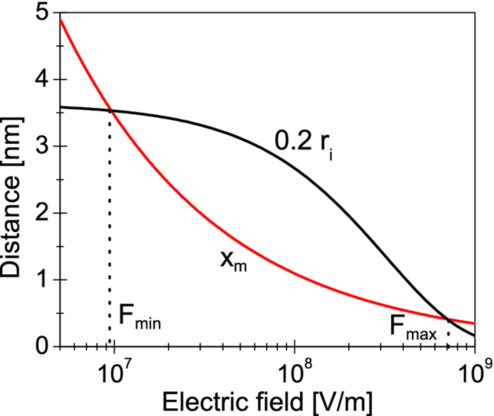 Fig. 2(a) Critical electric fields Fmin and Fmax at the interface, separating the validity of the SPD and MF approximations versus the injection barrier of the contact. The parameters are those used in Fig. 1. In the SP region below FL, where ri is smaller than the insulator thickness L (100 nm), the continuous description is by all means inappropriate. Above Flim, the Boltzmann statistics are violated (Ref. 17). (b) The associated validity chart in the plane of injection barrier and external bias. The dashed-dotted line indicates the critical injection barrier below which the MF approach is always valid. 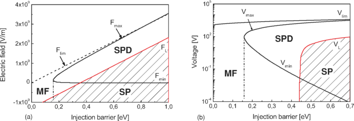 Using Eq. 3 in conjunction with the critical field values from Fig. 2 and the fact that the integral over the field along the MIM system yields the external voltage, a validity chart of the used SP, SPD, and MF approximations in the plane of external bias and the injection barrier can be established. The result is depicted in Fig. 2 as well. For the given example, the MF approximation holds over the entire voltage range as long as the injection barrier is <0.16 eV. With the growing Δ value, the bias window for the SPD region gains. Below Vmin, the MF approximation always holds because, at low bias, the reservoir of the enrichment contact is not depleted and the diffusion field at the contact does not allow for a Schottky effect at all. Above the line Vmax the barrier lowering due to the field penetration in the contact is so strong that, again, a substantial amount of carriers penetrate the insulator. The MF approximation holds again. In the striped SP region, the use of continuous particle densities is impossible because less than one carrier exists between the contact plates. 2.3.Modified Mean-Field ApproachThe deficit of the MF approximation to describe the carrier injection within the SPD regime but outside the striped parameter range results from the absence of the individual image force dragging on each single charge carrier. As long as xm < 0.2ri, such a strong but short-range deviation from the mean field near the interface can be modeled like a dipole layer, with a characteristic width xm. Because each injected charge carrier traversing the dipole layer needs to perform the work Δ–eδϕsch due to its individual image charge force, the electrostatic potential at the interface will be shifted by [TeX:] \documentclass[12pt]{minimal}\begin{document}\begin{equation}
\phi _i ( + 0) - \phi _{\rm c} ( - 0) = \delta \phi _{{\rm sch}}.
\end{equation}\end{document} Equation 10, defined at the interface between insulator and conductor, implies that the dipole layer is supposed to be infinitesimally thin, thus leading rather to a dipole jump of the electrostatic potential right at the interface. The resulting modified boundary condition at the interface thus reads [TeX:] \documentclass[12pt]{minimal}\begin{document}\begin{equation}
p_i \left( 0 \right) = N_i \exp \left\{ { - \frac{1}{{k_{\rm B} T}}\left[ {\Delta - eF_i \left( 0 \right)l_{{\rm TF}} \frac{{\varepsilon _i }}{{\varepsilon _{\rm c} }} - \left( {1 - \frac{{x_{\rm m} }}{{0.2r_i }}} \right)\delta \phi _{{\rm sch}} } \right]} \right\}
\end{equation}\end{document} where the effective barrier Δeff defined on basis of Eq. 5 is extended by the third term in the square brackets. Equation 11 holds in the SP region for max{Vmin, VL} ≤ V <min{Vmax, Vlim}. The empirical interpolation factor 1 – xm/(0.2 ri) simply provides a smooth transition between regimes.Because of the modification of the boundary condition, Fig. 2 must be reconsidered. Certainly, the critical voltages Vmin, Vmax do not change because, at these bias conditions, Eq. 5 is obtained. However, the unassailable SP regime framed by VL is supposed to shrink because the density of injected charge carriers will increase within the insulator. In the remaining SPD regime, the modified MF (MMF) approximation is now applicable. Despite the inviolable SP regime, the MMF approximation is suited to describe MIM systems across a large parameter space. The difference between the MMF-approximated drift-diffusion approach and the MF approximation is illustrated on basis of current voltage characteristics of a symmetric MIM system of ITO/intrinsic OS/ITO, assuming at both interfaces an injection barrier of 0.4 eV. The IV characteristics are depicted in Fig. 3. For both approximations, the IV characteristic is linear at low bias. The barrier lowering is small, and the contacts provide Ni exp[–Δ/kBT] carriers. Because the conductivity is independent from the bias, an ohmic behavior is observed. For voltages of >0.1 V, the MMF approach starts to deviate from the MF approach. As the Schottky lowering of the injection barrier exceeds the potential drop in the injecting electrode, a steeper increase in the current density is observed for the MMF approximation approaching the space-charge limit faster. The transition to the SCLC indeed appears now at voltages of ∼10 V, whereas the MF approximation yields a transition voltage of 100 V. In the SCLC regime, both characteristics merge again because the OS bulk (drift term), but not the contacts (boundary conditions), limits the current density. Fig. 3IV characteristic of an ITO/OS/ITO MIM diode assuming unipolar transport. Parameters are given in the captions of Fig. 1. The dotted lines are calculations using the MF approximation, and the continuous lines represent the results on basis of the MMF approximation. Calculations were done for an intrinic semiconductor and a charge-transfer-doped semiconductor with a doping level of 1017 cm−3. The dotted line indicates the quadratic voltage dependence of the SCLC. (Color online only). 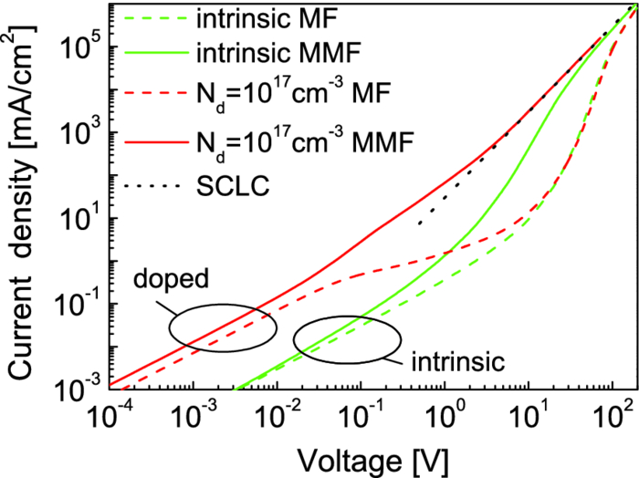 In Fig. 3, another example of a charge-transfer-doped OS within the very same MIM structure is shown. Be aware that depletion contacts develop in the considered case. The doping density of 1017 cm−3 increases, in the first place, the current density in the low-voltage regime if compared to the intrinsic case, but retains the ohmic behavior. This is due to the doping-induced background carriers providing a larger OS conductivity as the one embossed by the contacts. Yet, for the MF approach, the current density fades away above 10−2 V, approaching the characteristic of the undoped MIM system. The doping-induced carriers are depleted from the OS because the supply of carriers from the weak injecting contact is hampered. At increased voltage, the barrier lowering due to the voltage drop in the contact gains, the current increase growth again, and the current density approaches the SCLC regime. For the MMF approximation, such a dependence is not observed. The space-charge region within the depletion width at the injecting contact provides a substantial electric field. In conjunction with the MMF approximation and the associated Schottky lowering, the deliverance of carriers across the depletion contact is sufficient to prevent the depletion of the OS bulk. As a consequence, the high current density level is maintained. At higher voltages, space-charge effects set in again. The above-discussed topic is by far not restricted to OS but is also applicable to other insulators, such as inorganic dielectrics. The substantial material diversity opening wide parameter windows requires, however, the evaluation of the validity chart of each particular parameter set. An interesting parameter aspect is related to the prevailing dielectric constant of the insulator because it codetermines the strength of the barrier modifications given in Eq. 11. Because the dielectric constant of common organic materials is small, typically <10, the discrepancy between the MMF and MF approximations within the SPD regime is supposed to be stronger than for high-k materials. This is because the Schottky barrier lowering given by Eq. 6 shows a ɛi−1/2 dependence and thus growth with decreasing ɛi. At higher ɛi, the Schottky effect becomes less important and the IV characteristics of the MMF and MF approximations approach each other. This fact underlines the importance of the modified mean-field approach for the calculation of the electrical response of MIM systems based on organic semiconductors. 3.ConclusionsIn conclusion, the mean-field drift-diffusion approach used to describe the electrical device behavior of MIM systems has been critically reexamined in terms of prevailing single-particle effects. In particular, the Schottky effect has been recognized to be of crucial importance to appropriately describe the IV characteristic of MIM diodes. The transition region between the mean-field and single particle dominance was found by comparing mean-field and image charge contributions of the mean force on an individual carrier. The obtained validity charts in the bias/injection barrier plane show substantial SPD windows opening above a critical barrier with increased barrier height. For low and high external bias, the MF approach always holds because, in this region, large carrier densities are established in the insulator either due to charge-carrier diffusion from the contacts or due to severe barrier lowering, respectively. In order to be applicable in at least part of the emerged SP regime, the MF boundary conditions were extended to account for the Schottky effect. The resulting IV characteristics display a substantially improved behavior in the injection-limited regime with an improved transition voltage for entering space-charge limitation. The thus developed extension of the common drift-diffusion approach is not restricted to device design and shape or material classes discussed here. An extension to other devices, such as MIS diodes, field-effect transistors, photovoltaic cells, or to other materials or material systems is conceivable. Hence, the presented considerations here must be seen in a more general context than being restricted to organic electronics. AcknowledgmentsThis work was supported by the Deutsche Forschungsgemeinschaft through the Sonderforschungsbereich 595 and the BMBF funded Project TOPAS2012 (Project No. 13N10474). ReferencesL. J. A. Koster, E. C. P. Smits, V. D. Mihailetchi, and P. W. M. Blom,
“Device modle for the operation of polymer/fullerene bulk heterojunction solar cells,”
Phys. Rev. B, 72
(8), 085205
(2005). http://dx.doi.org/10.1103/PhysRevB.72.085205 Google Scholar
P. W. M. Blom, M. J. M. de Jong, and J. J. M. Vleggaar,
“Electron and hole transport in poly(p-phenylene vinylene) devices,”
Appl. Phys. Lett., 68
(23), 3308
–3310
(1996). http://dx.doi.org/10.1063/1.116583 Google Scholar
V. Kumar, S. C. Jain, A. K. Kapoor, W. Geens, T. Aernauts, J. Poortmans, and R. Mertens,
“Carrier transport in conducting polymers with field dependent trap occupancy,”
J. Appl. Phys., 92
(12), 7325
–7329
(2002). http://dx.doi.org/10.1063/1.1523142 Google Scholar
F. Neumann, Y. A. Genenko, R. Schmechel, and H. von Seggern,
“Role of diffusion on SCLC transport in double injection devices,”
Synth. Met., 150
(3), 291
–296
(2005). http://dx.doi.org/10.1016/j.synthmet.2005.03.005 Google Scholar
F. Neumann, Y. A. Genenko, C. Melzer, S. V. Yampolskii, and H. von Seggern,
“Self-consistent analytical solution of a problem of charge-carrier injection at a conductor/insulator interface,”
Phys. Rev. B, 75
(20), 205322
(2007). http://dx.doi.org/10.1103/PhysRevB.75.205322 Google Scholar
K. C. Kao and W. Hwang, Electrical Transport in Solids with Particular Reference to Organic Semiconductors, Pergamon Press, Oxford
(1981). Google Scholar
P. S. Davids, I. H. Campbell, and D. L. Smith,
“Device model for single carrier organic diodes,”
J. Appl. Phys., 82
(15), 6319
–6325
(1997). http://dx.doi.org/10.1063/1.366522 Google Scholar
S. M. Sze, Physics of Semiconductor Devices, Wiley, Hoboken, NJ
(1981). Google Scholar
G. G. Malliaras and J. C. Scott,
“The role of injection and mobility in organic light emitting diodes,”
J. Appl. Phys., 83
(10), 5399
–5403
(1998). http://dx.doi.org/10.1063/1.367369 Google Scholar
J. C. Scott and G. G. Malliaras,
“Charge injection and recombination at the metal–organic interface,”
Chem. Phys. Lett., 299
(2), 115
–119
(1999). http://dx.doi.org/10.1016/S0009-2614(98)01277-9 Google Scholar
V. I. Arkhipov, E. V. Emelianova, Y. H. Tak, and H. Bässler,
“Charge injection into light-emitting diodes: Theory and experiment,”
J. Appl. Phys., 84
(2), 848
–856
(1998). http://dx.doi.org/10.1063/1.368146 Google Scholar
M. N. Bussac, D. Michoud, and L. Zuppiroli,
“Electrode injection into conjugated polymers,”
Phys. Rev. Lett., 81
(8), 1678
–1681
(1998). http://dx.doi.org/10.1103/PhysRevLett.81.1678 Google Scholar
J. J. M. Van Der Holst, M. A. Uijttewaal, R. Balasubramanian, R. Coehoorn, P. A. Bobbert, G. A. de Wijs, and R. A. de Groot,
“Modeling and analysis of the three-dimensional current density in sandwich-type single-carrier devices of disordered organic semiconductors,”
Phys. Rev. B, 79
(8), 085203
(2009). http://dx.doi.org/10.1103/PhysRevB.79.085203 Google Scholar
F. Neumann, Y. A. Genenko, C. Melzer, and H. von Seggern,
“Self-conistent theory of unipolar charge-carrier injection in metal/insulator/metal systems,”
J. Appl. Phys., 100
(8), 084511
(2006). http://dx.doi.org/10.1063/1.2360383 Google Scholar
S. V. Yampolskii, Y. A. Genenko, C. Melzer, K. Stegmaier, and H. von Seggern,
“Bipolar charge-carrier injection in semiconductor/insulator/conductor heterostructures: self-consistent consideration,”
J. Appl. Phys., 104
(7), 073719
(2008). http://dx.doi.org/10.1063/1.2990051 Google Scholar
Y. A. Genenko, S. V. Yampolskii, C. Melzer, and H. von Seggern,
“Self-consistent phenomenological theory of charge injection at the conductor/insulator interface,”
Integr. Ferroelectr., 106 49
–60
(2009). http://dx.doi.org/10.1080/10584580903213225 Google Scholar
Y. A. Genenko, S. V. Yampolskii, C. Melzer, K. Stegmaier, and H. von Seggern,
“Charge carrier injection into insulating media: Single-particle versus mean-field approach,”
Phys. Rev. B, 81
(12), 125310
(2010). http://dx.doi.org/10.1103/PhysRevB.81.125310 Google Scholar
P. W. M. Blom and M. C. J. M. Vissenberg,
“Charge transport in poly(p-phenylene vinylene) light-emitting diodes,”
Mater. Sci. Eng., 27 53
–94
(2000). http://dx.doi.org/10.1016/S0927-796X(00)00009-7 Google Scholar
C. Melzer, V. V. Krasnikov, and G. Hadziioannou,
“Charge transport, injection and photovoltaic phenomena in oligo(phenylen vinylene) based diodes,”
J. Poly. Sci. Part B, 41
(21), 2665
–2673
(2003). http://dx.doi.org/10.1002/(ISSN)1099-0488 Google Scholar
E. Tutis, M.-N. Bussac, and L. Zuppiroli,
“Image force effects at contacts in organic light-emitting diodes,”
Appl. Phys. Lett., 75
(24), 3880
–3882
(1999). http://dx.doi.org/10.1063/1.125487 Google Scholar
E. Tutis, M. N. Bussac, B. Masenelli, M. Carrard, and L. Zuppiroli,
“Numerical model for organic light-emitting diodes,”
J. Appl. Phys., 89
(1), 430
–439
(2001). http://dx.doi.org/10.1063/1.1327286 Google Scholar
S. J. Martin, A. B. Walker, A. J. Campbell, and D. D. J. Bradley,
“Electrical transport characteristic of single-layer organic devices from theory and experiment,”
J. Appl. Phys., 98
(6), 063709
(2005). http://dx.doi.org/10.1063/1.2058199 Google Scholar
N. W. Ashcroft and N. D. Mermin, Solid State Physics, Thomson Learning, Florence
(1976). Google Scholar
D. Mergel and Z. Qiao,
“Dielectric modeling of optical spectra of thin In2O3:Sn films,”
J. Phys. D, 35
(8), 794
–801
(2002). http://dx.doi.org/10.1088/0022-3727/35/8/311 Google Scholar
D. Mergel and Z. Qiao,
“Correlation of lattice distortion with optical and electrical properties of In2O3:Sn films,”
J. Appl. Phys., 95
(10), 5608
–5615
(2004). http://dx.doi.org/10.1063/1.1704852 Google Scholar
H. Fujiwara and M. Kondo,
“Effects of carrier concentration on the dielectric function of ZnO:Ga and In2O3:Sn studied by spectroscopic ellipsometry: analysis of free-carrier and band-edge absorption,”
Phys. Rev. B, 71
(7), 075109
(2005). http://dx.doi.org/10.1103/PhysRevB.71.075109 Google Scholar
|


