|
|
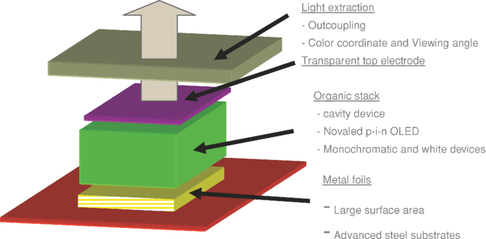
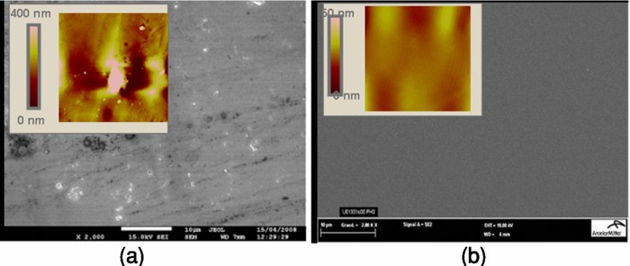
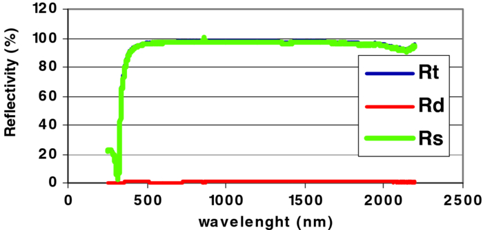
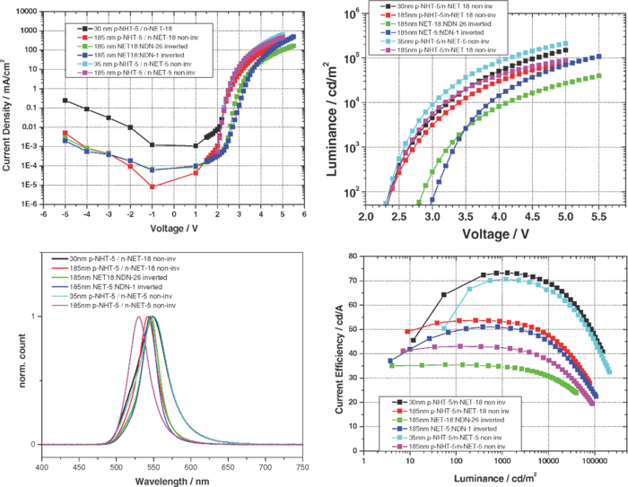
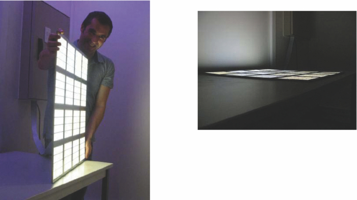
1.IntroductionOrganic light-emitting diodes (OLEDs) will provide a new generation of lighting sources.1, 2 This solid state light source is a “green-energy” source with low power consumption and high energy savings without using mercury. It is a low-cost technology that enables many nice applications, such as flexible and shaped panel, large-area sources, and diffuse and planar emission. OLEDs can be integrated to a variety of substrates, such as glass, plastic, or metal. Although glass material is the most conventional substrate to fabricate organic solid state lighting,3, 4, 5 steel material is a promising alternative because it provides many advantages at once versus plastic or glass.6, 7, 8 Metal will be a very good support for developing a novel lighting source panel. OLEDs on steel offer flexible, rigid, or even formable devices. Steel has very good oxygen- and water-barrier properties. It is a very good electrical and thermal conductor, which can greatly improve the lifetime of the device thanks to heat dissipation. And, devices on steel will be produced in a roll-to-roll process, which is a low-cost and competitive process. Several markets have already been identified: Automotive industry, appliance, general lighting, public lighting, signage, and obviously, other original flexible applications for the near future. Although several niche markets are promising, the general lighting market is the most promising market. Several physical properties have to be investigated to prepare OLEDs on metal foil (Fig. 1). This is a top-emitting device, where a rough surface over a large surface area must be taken into account. A specific treatment must be developed on metal foils. Moreover, thick organic electron and hole transport layers (ETL/HTL) can be n- and p-type doped.9, 10 Doped layers provide efficient carrier injection from both contacts into the doped transport layers and ohmic losses in those highly conductive layers are reduced dramatically. By combination of so-called doped PIN-OLEDs8 with advanced metal foils, high device performances are obtained with low driving voltage, high power, and luminous efficiencies. Furthermore, a transparent electrode with high conductivity is necessary to obtain constant current distribution over a large surface area.11 Last but not least, a light extraction solution must be developed to achieve good device performance.12 That will help to extract trapped light out of the device as well as to minimize the shift of color coordinates over viewing angle due to microcavity effect in such organic resonator devices.13, 14, 15, 16 Here we report improved large-area OLED devices. An advanced steel substrate for OLED integration is presented. We achieved high performances of monochromatic red, green, and blue devices integrated on steel, with a power efficiency of >70 lm/W at 1000 cd/m2 for the green color. In addition, we also show large white OLED panel lighting prototypes on metal foils with dimensions of – 600 × 600 mm2. 2.Advanced Steel SubstratesArcelorMittal has developed a new advanced steel substrate17 dedicated to OLED integration overcoming difficulties in lighting applications. It covers a large range of steel substrate types from highly polish steel, stainless steel, and copper foil. It is based on a multilayer and patterned coating. Some of the solutions are already manufactured in a continuous-roll process. Besides the advantages metal foils provide, several essential physical properties are required to reach high OLED device reliability. Prior to any device fabrication steps, the surface of the steel foil can be chemically or mechanically polished to reduce peak-to-peak and Ra surface roughness. It is first submitted to a cleaning process that would combine wet and dry processes in a clean-room environment. That consists of a bath of specific sequences of cleaning agents, mainly solvent for degreasing, and afterward, a treatment by reactive plasma. This cleaning step (and its sequence) is important to ensure device reliability. It will minimize defect density and remove contaminations. Thereafter, a first passivation system based on a multilayer system will ensure two mains functions. It will serve as a dielectric coating to electrically decouple the conductive substrate from both the anode and the cathode, and also acts as planarization layer of the steel surface. This passivation system must be able to fully cover the whole surface of the substrate to prevent any electrical shortcuts. The difficulty resides in macroapplication to prevent local defects at a microscale range or even lower. On the other hand, the planarization coating will drastically reduce the surface roughness, and gap or morphological defects will be covered at the surface. Images showing the surface before and after dielectric coating deposition are illustrated in Fig. 2. Figure 2 shows SEM and AFM images (tapping mode, 50 × 50 μm2) of a conventional tin-plated steel surface. The surface roughness values are Ra = 110 nm (Z range = 1645 nm) measured with AFM instrument. These values will not afford to make any reliable devices. Figure 2 shows SEM and AFM images (tapping mode, 50 × 50 μm2) after planarization of a steel surface. The surface roughness values are now measured to be Ra = 3.3 nm (Z range = 25 nm). Such surface roughness is ensured on a large surface area as demonstrated by the SEM images. Note that the upper limit value of Ra = 10 nm is empirically imposed in order to reach reliable devices. In order to evaluate the quality of the coating, the leakage current is measured through a metal-insulator-metal (MIM) junction, formed by the conductive surface, the dielectric multilayer coating, and some topmost evaporated Ag pads (10 mm2). Those metallic pads are spatially and uniformly distributed on the surface to form a matrix network, as indicated in Fig. 3. As an example, on a 150 × 150 mm2 surface with 36 pads, a leakage current of <0.1 μA at 10 V was measured (lower limit of the Keithley 2400), indicating very good insulating properties across the surface without cracks or an electrical short circuit. It was verified that the MIM junctions are not altered, even after applying a voltage of 220 V. Note that a lower limit has been fixed at 10−6 mA/cm2 in dc current. The latter value is much lower than the leakage current measured on an OLED device. Note also that this measurement can be taken any substrate sizes, which allows evaluating larger foils from line processing. Fig. 3Leakage current measurement of large surface area through MIM junction (Ileakage < 10−6 mA/cm2). 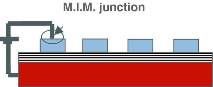 Top-emitting OLEDs can be tuned to emit more light in the forward direction. In this case, a resonant cavity is formed in which the anode and the semitransparent cathode act as the mirrors of the microcavity. The distance between the two mirrors is defined by the organic layer thickness. The resonant cavity is thus tuned, and spontaneous emission of emitters in all top-emitting devices can be enhanced. The bottom electrode, conventionally the anode, can consequently be improved by offering a high optical reflectivity and low absorption coefficient. Figure 4 illustrates typical optical reflectivity curves measured using a Varian Instrument. Spectra show a high total reflectivity value of >95% in the visible range, with a diffuse component equal to zero. Such a condition is reached because the reflective electrode is deposited onto the coated advanced steel surface with a very low roughness value. 3.Organic Light-Emitting Diodes Device on Metal Foils3.1.Monochrome-Emitting DevicesThe typical structure of monochromatic devices is shown in Fig. 5: Advanced steel/p-type-doped HTL/interlayer on hole side, emission layer (guest and phosphorescent emitters host)/interlayer on electron side, n-type doped ETL/semitransparent cathode-capping layer. Fig. 5Typical energetic diagram used for monochromatic devices. (For doped transport layers, band bending is observed at both electrode junctions, which is not shown here.) 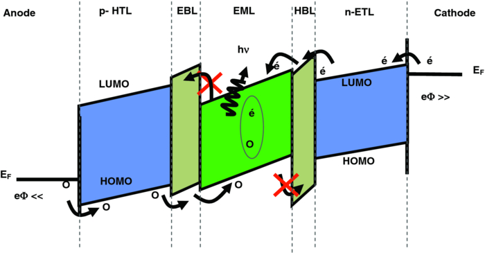 Doped transport layers have two main advantages.9 First, high conductivity is reached. The device operates close to flatband condition. The IV characteristics are then determined by space-charge-limited conduction instead of injection-limited conduction.18 Second, a thin and high-energy tunneling barrier is produced between the transport level of the semiconductor and contact metal by band bending. The contact at this interface is thus considered as an ohmic contact, which allows the use of several different metallic materials with different work functions. This is in contrast to undoped transport layers, where charge injection depends more strictly on the material's work function; thus, the carriers must overcome the barrier at the interface. It is possible to improve operating voltage and efficiency by the insertion of a thin organic interlayer. Electron-blocking layer (EBL), and hole-blocking layer (HBL) adjacent to the emission layer. This will prevent the formation of nonradiative recombination paths. With an energetic diagram of organic material carefully chosen, a blocking layer exhibits a LUMO (respectively, HOMO) higher (respectively, lower) than the corresponding energy level of the emission layer host. In that case, penetration of electrons (respectively, holes) into the HTL (respectively, ETL) is prevented. In other words, the interlayers confine the charge carriers (and excitons) in the emission zone and further prevent exciplex formation. Figure 6 shows J–V–L characteristics for a set of green-emitting PIN-OLEDs, where ETL and HTL thicknesses as well as the nature of materials were varied. In this case, for p-HTL and n-ETL layers, we use Novaled portofolio material: Novaled hole-transport (NHT) and Novaled electron-transport (NET) layers (commercial Novaled material designation). Moreover, we compare both inverted (from anode to anode), and noninverted (from cathode to anode) structures. Cathode material can be based on one monolayer semitransparent metallic material or on a multilayer system in order to optimize the electrical conductivity of the trnaparent cathode. This device exhibits excellent current–voltage curves with exponential behavior up to current densities of a few tens of milliamps per centimeters squared. It attains efficient carrier injection, with low leakage current as observed in the backward range. The brightness of 1000 cd/m2 is reached at a very low operating voltage of 2.5–3.5 V, which approximately corresponds to the energy of the green photons emitted from this device. The current efficiency reaches values of >70 cd/A. Devices are optimized by selecting HTL and ETL materials, dopant materials, and transport layer thicknesses as indicated in the legend of Fig. 6. In this example, two types of dopant are used, NDN 26 and NDN 1 (Novaled commercial designation), with two types of electron transport layers NET 18 and NET 5 (Novaled commercial designation). On the basis of the assumption that the contact at this interfaces is purely an ohmic contact, optical and electrical properties are decoupled. We can consequently tune the resonant cavity with different HTL and ETL thicknesses on the identical devices. Equivalent inverted structures have also been evaluated. Compared to noninverted structures, similar good performance was obtained but luminous power efficiency and current efficiency of inverted structures did not fully reach values measured in noninverted samples. 3.2.White-Emitting DevicesA first simple white OLED with doped hole and electron transport layers was realized thanks to two color emissive layers (blue and yellow). Figure 7 shows the respective EL emission spectrum. Fig. 7J–V–L characteristics of white PIN-OLED devices on advanced steel substrate. The brightness of 1000 cd/m2 is reached at a very low operating voltage of 3–5 V. The power efficiency at a brightness of 1000 cd/m2, 22 lm/W, and 25 lm/W is demonstrated. Color coordinates are CIE-x = 0.38–0.40 and CIE-y = 0.39–0.41. 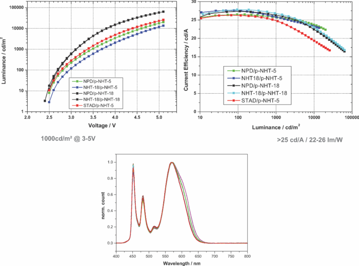 This device also exhibits already remarkable excellent current–voltage–luminance curves (Fig. 7). Here again, in this example we compare transport layer and dopant materials. It attains efficient carrier injection with low leakage current. The brightness of 1000 cd/m2 is reached at a very low operating voltage of 3–5 V. Although, the power efficiency at a brightness of 1000 cd/m2 is generally ∼10 lm/W, here we measure to up to 22 lm/W (NHT 5) and 26 lm/W (NHT 18), within integrated sphere. Warm white emission can be obtained (Fig. 7). In contrast to monochromatic devices, the microcavity effect significantly alters the white OLED performances. Variations of the cavity thickness disturb white emission white spectra and shift the color coordinate over the viewing angle due to interference phenomena. One way to correct this dependence is the use of an external scattering layer. Several kinds of materials have been screened for use as a capping layer to replace the commonly used NPD. NLE–17 material [Novaled light-extraction layer (NLE)] gives very uniform emission over angle with color coordinates at illuminant A, even in the case of thin metallic top contacts. This cap layer enhances light outcoupling by a factor of 1.5. 3.3.Large-Area PanelOn the basis of preliminary WOLED (white OLED) on steel performance, we were able to build lighting panels first, as shown in Fig. 8. As an example, the presented OLED lighting panel with dimensions of 60 × 60 cm, emits white light at illuminant A. Complex light scenarios can be adjusted by the driver setup. 4.ConclusionIn this work, we have briefly shown and discussed the OLED device integration on metal foils for lighting applications. The optimization of the devices needs the tailoring of the physical properties of metal foil. Such an original advanced steel substrate has been developed by ArcelorMittal Research. It covers several functionalities, such as high optical reflectivity, low roughness surfaces, high electrical insulator barrier over a large surface area, and a high anode electrical conductivity of the anode. In order to evaluate the advanced foils, doped transport layers, so-called PIN-OLEDs, have been used. This combination leads to very high OLED performances working at low voltage. Power efficiencies at 1000 cd/m2 of >70 lm/W for monochromatic and 22–26 Lm/W for white color have been measured. AcknowledgmentsThis work is financially supported by Wallon Region (Marshall plan), and the authors thank, in particular, all partners involved. ReferencesN. Ide, H. Tsuji, N. Ito, H. Sasaki, T. Nishimori, Y. Kuzuoka, K. Fujihara, T. Miyai, and T. Komoda,
“High-performance OLEDs and their application to lighting,”
Proc. SPIE, 7051 705119
(2008). http://dx.doi.org/10.1117/12.798190 Google Scholar
V. van Elsbergen, H. Boerner, H.-P. Löbl, C. Goldmann, S. Grabowski, E. Young, G. Gaertner, and H. Greiner,
“OLEDs for lighting applications,”
Proc. SPIE, 7051 70511A
(2008). http://dx.doi.org/10.1117/12.797457 Google Scholar
R. F. Service,
“Organic LEDs look forward to a bright, white future,”
Science, 310
(5755), 1762
–1763
(2005). http://dx.doi.org/10.1126/science.310.5755.1762 Google Scholar
S. R. Forrest,
“The path to ubiquitous and low-cost organic electronic appliances on plastic,”
Nature, 428 911
–918
(2004). http://dx.doi.org/10.1038/nature02498 Google Scholar
S. Reineke, F. Lindner, G. Schwartz, N. Seidler, K. Walzer, B. Lüssem, and Karl Leo,
“White organic light-emitting diodes with fluorescent tube efficiency,”
Nature, 459 234
–238
(2009). http://dx.doi.org/10.1038/nature08003 Google Scholar
C. C. Wu, S. D. Theiss, G. Gu, M. H. Lu, J. C. Sturm, S. Wagner, and S. R. Forrest,
“Integration of organic LED's and amorphous Si TFT's onto flexible and lightweight metal foil substrates,”
IEEE Electron Device Lett., 18
(12), 609
–612
(1997). http://dx.doi.org/10.1109/55.644086 Google Scholar
N. Yamada, S. Koga, Y. Kubo, T. Hamada, S. Nagasaki, and T. Ishi,
“Nippon Steel,”
(2006). Google Scholar
Ph. Guaino,
(2009) Google Scholar
M. Pfeiffer, K. Leo, X. Zhou, J. S. Huang, M. Hofmann, A. Werner, and J. Blochwitz-Nimoth,
“Doped organic semiconductors: Physics and application in light emitting diodes,”
Organic Electronics, 4 89
–103
(2003). http://dx.doi.org/10.1016/j.orgel.2003.08.004 Google Scholar
J. Kido and T. Matsumoto,
“Bright organic electroluminescent devices having a metal-doped electron-injecting layer,”
Appl. Phys. Lett., 73 2866
–2868
(1998). http://dx.doi.org/10.1063/1.122612 Google Scholar
J. Birnstock, A. Lux, M. Ammann, P. Wellmann, M. Hofmann, and T. Stübinger,
“Novel materials and structures for highly-efficient, temperature-stable, and long-living AM OLED sisplays,”
SID Int. Symp. Digest Tech. Papers, 37 1866
–1869
(2005). Google Scholar
Ulrich Todt, Y. Sun and S. R. Forrest,
“Enhanced light out-coupling of organic light-emitting devices using embedded low-index grids,”
Nat. Photon., 2 483
–487
(2010) http://dx.doi.org/10.1038/nphoton.2008.132 Google Scholar
M. Thomaschke, R. Nitsche, M. Furno, and K. Leo,
“Optimized efficiency and angular emission characteristics of white top-emitting organic electroluminescent diodes,”
Appl. Phys. Lett., 94 083303
(2009). http://dx.doi.org/10.1063/1.3088854 Google Scholar
C.-C. Liu, S.-H. Liu, K.-C. Tien, M.-H. Hsu, H.-W. Chang, C.-K. Chang, C.-J. Yang, and C.-C. Wu,
“Microcavity top-emitting organic light-emitting devices integrated with diffusers for simultaneous enhancement of efficiencies and viewing characteristics,”
Appl. Phys. Let., 94 103302
(2009). http://dx.doi.org/10.1063/1.3097354 Google Scholar
Q. Huang, S. Reineke, K. Walzer, M. Pfeiffer, and K. Leo,
“Quantum efficiency enhancement in top-emitting organic light-emitting diodes as a result of enhanced intrinsic quantum yield,”
Appl. Phys. Let., 89 263512
(2006). http://dx.doi.org/10.1063/1.2425014 Google Scholar
S. Reineke, F. Lindner, G. Schwartz, N. Seidler, K. Walzer, B. Lussem, and K. Leo,
“White organic light-emitting diodes with fluorescent tube efficiency,”
Nature, 459 234
–238
(2009). http://dx.doi.org/10.1038/nature08003 Google Scholar
Ph. Guaino, F. Maseri, and L. Avril,
“ArcelorMittal Liege Research,”
(2010). Google Scholar
J. Kalinowski, Organic Light-Emitting Diodes, Principles, Characteristics, and Processes, Marcel-Dekker, New York
(2005). Google Scholar
|