|
|
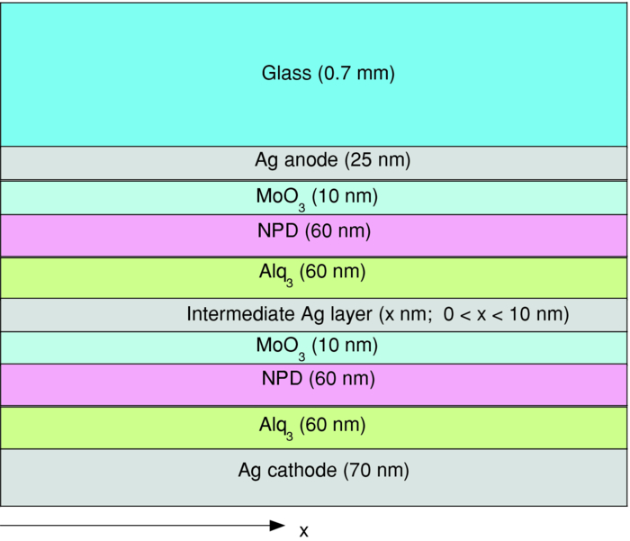
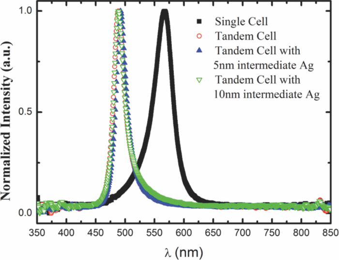
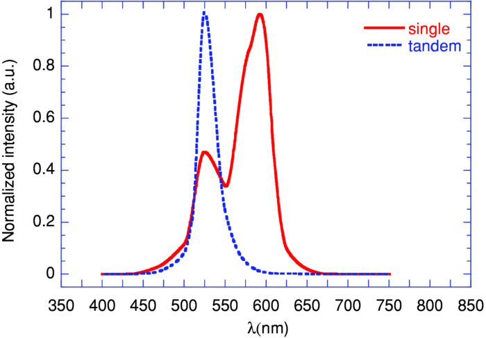
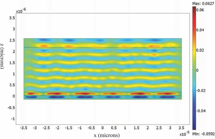
1.IntroductionMicrocavity organic light-emitting diodes (OLEDs) have attracted much attention since they have a number of properties that are superior to common single-unit OLEDS. Cavity OLEDs have a resonant cavity generated by partially reflecting surfaces, within which the emitting layer lies. The resonant modes of the cavity occur when integer multiples of half a wavelength can fit within the cavity. When the resonant modes of the cavity lie within the spectrum of the organic emitter a number of sharp wavelengths can be emitted from the cavity. Utilizing multiple wavelength emission from a cavity has been demonstrated to be a viable solution for achieving white light OLEDs.1, 2, 3, 4 Tandem OLEDs are formed by combining in series single units5, 6 separated by a charge generation layer (CGL), analogous to tandem solar cells. Tandem OLEDs with different emitting species in each repeat unit can generate multiple wavelength emission, which can be combined to generate white light. If the same emitting species is incorporated in each repeat unit, narrower electroluminescence (EL) spectra may be obtained. OLED architectures combining microcavities with tandem structures have been shown3, 5 to yield strong enhancement in efficiency. This paper describes the results of simulations of the emission from microcavity tandem OLEDs, using rigorous finite element and Fourier space solutions of Maxwell's equations, and compares them to experimental results. Good agreement with the experimental results is obtained, and the potential of this simulation approach to predict the properties of more complex OLED architectures is discussed. 2.ResultsThe basic single OLED unit (“UNIT A,” does not include the electrodes) was 10-nm MoO3/60 nm [N,N′-bis(naphthalen-1-yl)-N,N′-bis(phenyl)benzidine (α-NPB)/60-nm tris (8-hydroxyquinoline)] Al (Alq3), where, α-NPB is a standard hole-transporting layer and Alq3 is a standard emitting and electron-transporting layer. Recombination of excitons occurs within the Alq3 layer very close (0 to 10 nm) to the α-NPB/Alq3 interface. The microcavity single unit OLED was 0.7-mm glass/25-nm semitransparent partially reflecting Ag anode/UNIT A/1-nm LiF/1-nm Al / 70-nm reflecting Ag cathode. The microcavity 2-unit tandem OLED (Fig. 1) was 0.7-mm glass/25-nm semitransparent partially reflecting Ag anode/UNIT A/1-nm LiF/x-nm Ag/UNIT A/1-nm LiF/1nm Al/70-nm reflecting Ag cathode. The intermediate Ag layer, of thickness 0 ≤ x ≤ 10 nm, was added to enhance the CGL between the two units and explore its potential effect on the device's optical properties. Transition metal oxides have alternatively been used as a CGL between stacked OLEDs.6 2.1.Experimental Results on the Fabricated OLEDsTandem and single cavity OLEDs were fabricated by standard thermal evaporation techniques on 0.7-mm thick glass substrates. The most notable feature in the measured front EL spectra was a peak near 560 nm for the microcavity single unit OLED that blueshifted to 480 nm in the microcavity tandem device (Fig. 2). The spectrum of the latter was also considerably narrower than Fig. 2. As clearly seen, the intermediate Ag layer had no effect on the peak wavelength or width of the EL spectrum. 2.2.Simulation Results With Real-Space Solutions of Maxwell's EquationsWe first performed simulations of the microcavity single and tandem OLEDs by finite-element solutions of Maxwell's equations in real space within the COMSOL simulation package. Experimental values of the frequency-dependent dielectric functions were utilized for individual layers. Spectroscopic ellipsometry measurements7 provided the wavelength-dependent dielectric functions of Alq3 and α-NPB throughout the relevant wavelength range (400 to 800 nm). In the simulations, a distribution of emitting sources, represented by small dipoles, were placed near the interface of Alq3 and α-NPD, to simulate the stochastic nature of light emission in the OLED. The emitting dipole sources were placed uniformly along the x-direction of the OLED (Fig. 1). The orientational distribution of dipole sources is random so that the dipoles sample all the orientations in the planes parallel and perpendicular to the plane of Fig. 1, as found for Alq3.8 We do not assume a preferred dipole orientation as found for blue emitting materials.8 Both polarizations of the field were simulated. The structure was discretized with an adaptive real space grid. Since the glass is far thicker than the rest of the structure, the calculations were done for a thinner glass substrate (2 μm) to determine the electric and magnetic fields, at the upper air boundary of the structure. The near-to-far field transformation was done to extend these field components to infinity. This accurately determines the fields in the air region and takes into account the trapped wave-guided modes inside the glass. The field of each individual current source is calculated in the far-field. Since the individual sources are incoherent, the field intensities are added to obtain the resulting far-field emitted intensities. For computational convenience, the calculation was performed for all sources at the same time rather than the equivalent procedure of performing the calculation for each source individually and summing the results. The computational domain spanned 7 μm in the x-direction. The far-field emitted intensity was calculated at each wavelength to obtain the transmitted field intensity. That intensity was multiplied by the experimentally known emission profile of the Alq3 emission that peaks at ∼525 nm, to obtain the resulting far-field emitted intensity, which can then be directly compared to the experimental EL. The transmitted field for a microcavity single unit OLED has a primary peak near 600 nm [Fig. 3]. The optical length of the single cavity is ∼260 to 300 nm, so the 600-nm peak represents the fundamental n = 1 mode where half a wavelength fits within the cavity. In addition there is a small peak at 520 nm. The tandem OLED, with an intermediate Ag thickness x = 10 nm, has two peaks in the transmitted field intensity near 520 and 720 nm [Fig. 3]. These two wavelengths represent two different resonant modes in the microcavity. The tandem OLED has an optical length of ∼520 nm so the 520 nm peak is a n = 2 mode. After convolution with the Alq3 emission profile the 720-nm peak is suppressed and we are left with the microcavity tandem OLED having a peak near 520 nm, compared to the microcavity single unit device having a peak at 590 nm (Fig. 4). There is a small peak in the simulated emission intensity for the single cavity at 520-nm, as evident in the transmitted intensity. This 520-nm peak is not present in experiment. We interpret the origin of the 520-nm peak as arising from the convolution of a sharply peaked source profile with the transmittance function which magnifies small features of the transmittance at the wavelength of 520 nm. The values of the peak emission wavelengths [520 nm (tandem), 590 nm (single)] compare reasonably well with experimentally measured values of 490 nm (tandem) and 570 nm (single). The peak width of the tandem OLED is narrower than the single OLED (Fig. 4) consistent with the experimental results (Fig. 3). Fig. 3(a) Simulated transmitted electric field intensity for a single OLED. (b) Simulated transmitted field intensity for a tandem OLED with an intermediate Ag thickness of x = 10 nm. 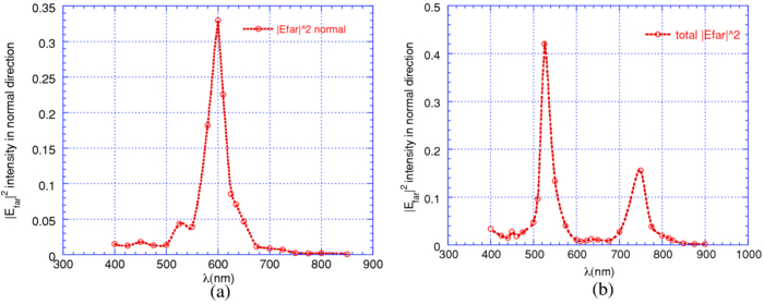 The redshift of the simulated values compared with measurement may be due to slight differences between the individual α-NPB and Alq3 layer thicknesses (60 nm each) utilized in the calculation and those fabricated. We have verified that reducing the NPB and Alq3 layer thicknesses to 40-nm blueshifts the simulated peak wavelengths to lower values. The intensity profile (Fig. 5) shows considerable emission in the normal direction traversing through the glass region, with the separation between the maxima in intensity corresponding to half the wavelength of the wave in the glass and air regions. The results are equivalent to performing simulations for each source sequentially and adding the intensities incoherently. 2.3.Results With the Scattering Matrix SimulationWhile the previous real-space solutions (Sec. 2.2) are a direct approach to simulating OLED emission, they are laborious to perform for optimizing OLED geometries. Furthermore the distribution of dipole orientations is approximated by the discretization within the real space grid and better averages over dipole orientations are required. For these reasons we have developed an alternative, powerful, fully parallelized technique for simulation and design of OLEDs based on rigorous solutions of Maxwell's equations in a plane wave basis, i.e. in Fourier space. This technique allows far faster optimization of OLED geometries for design problems. This technique is based on a scattering matrix method that has been very successful in simulation of optical properties of photonic crystals9, 10, 11, 12 and we show for the first time that it can be applied to OLEDs. In each layer of the OLED stack, the materials are represented by realistic frequency-dependent absorptive dielectric functions obtained from experimental measurements for Alq3 and NPD,7 by measurements for Ag,13 with measurements for ITO14 and MoO3.15 In the scattering matrix formalism the OLED is composed of layers stacked in the z direction. Rather than assuming that all layers are planar in the (x,y) plane we adopt a more general formalism where the layers can have a periodic structure in the planar (x,y) directions with a repeat vector R = n1a1 + n2a2, with lattice vectors a1 and a2. This general formalism allows for the investigation of out-coupling of trapped modes inside the glass using periodic microlens structures or out-coupling of organic/ITO modes with grating structures at the ITO-glass interface, which we plan for later studies. Within each layer of the OLED structure the dielectric function is ɛ(x,y): a function of x and y but not a function of z, so the dielectric function has the Fourier expansion of [TeX:] \documentclass[12pt]{minimal}\begin{document}\begin{equation}
\varepsilon (r) = \sum\limits_G {\varepsilon ({\bf G})e^{i{\bf G} \bullet {\bf r}} }\vspace*{-7pt}
\end{equation}\end{document} where G are the reciprocal lattice vectors of the system. The electric and magnetic fields are also expanded in Fourier components with strengths represented by lowercase symbols (e,h):
[TeX:] \documentclass[12pt]{minimal}\begin{document}\begin{equation}
E_\alpha ({\bf r}) = \sum\limits_{i = 1}^{NG} {e_{Gi,\alpha }(z)\exp [ - i({\bf k} + {\bf G}_i })\cdot {\bf x}_{||}],
\end{equation}\end{document} where k is a Bloch vector, and α is the Cartesian component, with an analogous expansion for the magnetic field.The source inside the OLED is treated through the well-developed formalisms of Whittaker and Culshaw,16 and Rigenault17 as a point dipole at position (r0,z0) at the interface of the e-transporting (Alq3) and hole-transporting (NPB) layers, with a current density J(r). The localized current can then be expanded in a Fourier series:16, 17 [TeX:] \documentclass[12pt]{minimal}\begin{document}\begin{equation}
{\bf J}(r,z) = {\bf J_0} \delta (r - r_0)\delta (z - z_0) = \sum\limits_{k,G} {{\bf j_k} ({\bf G})\exp [i({\bf k} + {\bf G}) \cdot r]\delta (z - z_0 }),
\end{equation}\end{document}
where jk(G) = J0exp [ − i(k + G) · r0].The localized source is converted into a superposition of periodic sources with the same amplitude but differing phase. With the OLED source term, Maxwell's equations for each frequency ω are [TeX:] \documentclass[12pt]{minimal}\begin{document}\begin{equation}
{\bm\nabla} \times {\bf H} = {\bf J} - i\omega \varepsilon (r){\bf E},
\end{equation}\end{document}
[TeX:] \documentclass[12pt]{minimal}\begin{document}\begin{equation}
{\bm\nabla} \times {\bf E} = i\omega {\bf H}.
\end{equation}\end{document}
In Fourier space Maxwell's equations can be compactly written as
[TeX:] \documentclass[12pt]{minimal}\begin{document}\begin{equation}
i{\mathop k\limits^ \wedge} _y h_z (z) - h_y' (z) = j_x \delta (z - z_0) - i\mathop \varepsilon \limits^ \wedge e_x (z),
\end{equation}\end{document}
[TeX:] \documentclass[12pt]{minimal}\begin{document}\begin{equation}
h_x' (z) - i{\mathop k\limits^ \wedge} _x h_z (z) = j_y \delta (z - z_0) - i\mathop \varepsilon \limits^ \wedge e_y (z),
\end{equation}\end{document}
[TeX:] \documentclass[12pt]{minimal}\begin{document}\begin{equation}
i{\mathop k\limits^ \wedge} _x h_y (z) - i{\mathop k\limits^ \wedge}_y h_x (z) = j_z \delta (z - z_0) - i\mathop \varepsilon \limits^ \wedge e_z (z),
\end{equation}\end{document} where jka are the Fourier components of the currents (which vanish outside the source layer). The lowercase (e,h) are the Fourier components of the electric and magnetic fields.At all layers, with the exception of the layer containing the sources, the parallel components of the fields (Ex, Ey) and (Hx, Hy) are continuous. However at the layer containing the source the parallel component of the fields are discontinuous. For dipole moments oriented in the plane (Jz = 0) the discontinuity of (Hx, Hy) is related to the current (jy, jx),16 [TeX:] \documentclass[12pt]{minimal}\begin{document}\begin{equation}
\begin{array}{l}
e_{||} (z_0^ +) - e_{||} (z_0^ -) = 0, \\[6pt]
h_{||} (z_0^ +) - h_{||} (z_0^ -) = p_{||}. \\
\end{array}
\end{equation}\end{document} For dipole moments oriented in the z-direction (Jx = 0 = Jy) the boundary conditions are that the discontinuity of (Ex, Ey) related to the curl of the currents.16
[TeX:] \documentclass[12pt]{minimal}\begin{document}\begin{equation}
\begin{array}{l}
e_{||} (z_0^ +) - e_{||} (z_0^ -) = p_z, \\[10pt]
h_{||} (z_0^ +) - h_{||} (z_0^ -) = 0. \\
\end{array}
\end{equation}\end{document} Here p∥ and pz are in-plane and z-components of the dipole moment in the emitting layer.16Thus this formalism allows for the radiation rates to be dependent on the local fields inside the emissive layer, a feature necessary to realistically describe OLEDS and enhanced emission intensities. The discontinuity of the fields can be combined with the scattering matrix formalism. For an arbitrary oriented dipole p at the interface between layers l and l + 1 the boundary conditions become [TeX:] \documentclass[12pt]{minimal}\begin{document}\begin{equation}
\begin{array}{l}
e_{||}^{l + 1} (0) - e_{||}^{l + 1} (d_l) = p_z, \\[6pt]
h_{||}^{l + 1} (0) - h_{||}^{l + 1} (d_l) = p_{||}. \\
\end{array}
\end{equation}\end{document} The remaining layers can be treated within a transfer matrix formalism developed by many authors.9, 10, 11, 12 Within each layer the fields satisfy the transfer matrix equations which can can be compactly written,
[TeX:] \documentclass[12pt]{minimal}\begin{document}\begin{equation}
\frac{\partial }{{\partial z}}E = M_1 H;\frac{\partial }{{\partial z}}H = M_2 H,
\end{equation}\end{document}
[TeX:] \documentclass[12pt]{minimal}\begin{document}\begin{equation}
\frac{{\partial ^2 }}{{\partial z^2 }}E = M_1 M_2 E,
\end{equation}\end{document} where
[TeX:] \documentclass[12pt]{minimal}\begin{document}\begin{eqnarray}
\frac{\partial }{{\partial z}}E_{G,x} = - \frac{{i(k + G)_x }}{{\omega /c}}\sum\limits_G {\varepsilon ^{ - 1} (G,G')[ {(k + G')_x H_{G',y} - (k + G')_y H_{G',x} } ]} - i(\omega /c)H_{G,y}\nonumber\\
\end{eqnarray}\end{document} defines the transfer matrix M1 for each layer, with a similar expression for M2.This eigenvalue equation 13 for the matrix M = M1M2 is solved in each layer to obtain eigenmodes. The boundary condition is enforced that parallel components of the fields are continuous at each interface. This leads to individual scattering matrices for each layer. A standard convolution algorithm11 combines the individual scattering matrices to provide the scattering matrix linking the emissive layer (l) to the air region.11 Multiple reflections are automatically accounted for in this formalism. The dipole can be oriented randomly in the three-dimensional space and can be located at different spatial locations within the OLED. In the absence of a microlens or periodic structure within the OLED all spatial locations are equivalent. The simulation of emitted fields is repeated for each (i) orientation, and (ii) spatial position of the dipole, to obtain the emitted field intensity outside the OLED, which is summed to get the total field intensity outside the OLED over all emission angles. Within the geometry chosen for the OLED (Fig. 1) x and y dipole orientations represent p-polarized emission and z-dipole orientation represents s-polarization. The simulation for each orientation and spatial position involves a sum over (a) Bloch vectors and a (b) finite set of reciprocal lattice vectors G. This rigorous solution of Maxwell's equations inside the OLED explicitly accounts for the reflected electric fields at the position of the dipole, that modify the radiation rate of dipoles in the OLED over their free-space value—an essential feature of OLED emission.18 However, it does not account for the reabsorption and re-emission of photons within the OLED layer since our simulation is done for a single source at each spatial position. This scattering matrix algorithm is routinely used in transmission and reflection of waves from photonic crystals when illuminated externally9, 10, 11, 12, 19 without an internal source. The algorithm differs from the approach of calculating reflection and transmission from a layered structure with a gain layer, which does not consider enhancement of radiation rates from local fields. Our scattering matrix formalism has many common features with the real-space transfer matrix simulations of Nowy,18 which also emphasizes the need for modifying radiation rates with local field enhancements. We first simulate the reflection and absorption for plane waves incident normally on the glass side of the OLED, with no emissive dipoles. These simulations show the microcavity modes at 530 and 730 nm for the tandem OLED compared to 600 nm for the single unit OLED (Fig. 6), as evidenced by sharp reflection minima and absorption maxima. Fig. 6Simulated reflection and absorption for (a) tandem and (b) single OLEDs with the scattering matrix method, showing the presence of microcavity modes. 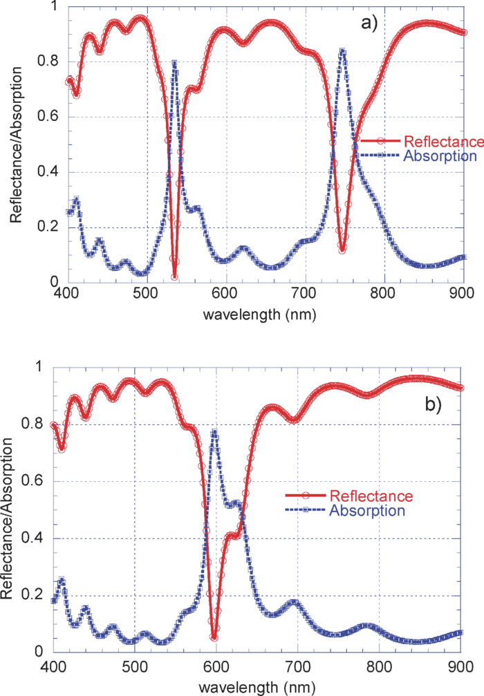 The simulated fields from tandem OLEDs also show maxima at 530 nm (Fig. 7). When the fields are convoluted with the Alq3 source emission profile this generates the normal emission at 520 nm for the tandem and ∼560 nm for the single unit OLED (Fig. 7). The total emission in all directions is broader (Fig. 7), displaying maxima at 525 nm for the tandem and 550 nm for the single unit OLED. This is in reasonable agreement with experimental measurements. Under these conditions the emissive layer lies at the antinode of the electric fields as found in earlier studies of tandem OLEDs.5 As discussed in Sec. 2.3, for the single cavity OLED (Fig. 7) there is an additional peak in the normal emission at 520 nm, which results from convoluting the emitted intensity with the source profile which has a peak at 520 nm, and provides an additional small peak at this wavelength. The shoulder at 590 nm (Fig. 7) for the single cavity device arises from the microcavity mode at this wavelength observed in the reflectance/absorption simulation [Fig. 6]. Additional smaller peaks at shorter wavelengths below 500 nm do appear. The peak width of the normal emission tandem OLED (∼18 nm) is narrower than the single OLED [∼34 nm, Fig. 7] consistent with the experimental results (Fig. 2), that find peak widths of 22 and 40 nm for the tandem and single devices, respectively. Roughness of interfaces in the device can broaden peak widths in experiment compared to simulation. Fig. 7Simulated normal emission and total emission (over all angles) from microcavity tandem and single unit OLEDs. The source profile of Alq3 emission is utilized. Averaging is performed for dipole sources in the upper and lower unit cells. 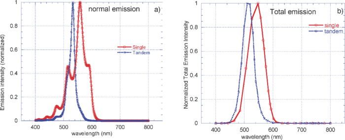 The thickness of the organic layers controls the microcavity properties. As mentioned earlier (Sec. 2.2) this organic layer thickness of 120 nm corresponds to an optical thickness of (260 to 300 nm) or ∼λ/2 for each unit, or for the single-cavity structure, and λ for the tandem structure. The emission spectrum of the microcavity OLEDs changes with the viewing angle as found in recent studies.20, 21, 22 Hence we simulated the angular emissivity of our microcavity OLEDs. For the single microcavity device we find [Fig. 8] the peak in the simulated angular emission spectrum occurring at 560 nm in the normal direction shifting to a stronger peak at 540 nm at a larger viewing angle around 40 deg in s-polarization, similar to the results found by Reinke20 for microcavity OLEDs. There is also an additional narrow peak at 520 nm for larger viewing angles of 50 to 60 deg. In comparison the angular variation is smoother in p-polarization with the peak emission occurring at 570 nm in the normal direction moving to a stronger peak near 560 nm between 10 and 30 deg [Fig. 8]. The p-polarized emission is weaker than the s-polarized emission, similar to the results of Wehlus22 and Reinke20 Fig. 8Emitted field intensity as a function of emission angle for the single microcavity OLED in (a) s and (b) p-polarizations. Emitted field intensity as a function of emission angle for the tandem microcavity OLED in (c) s and (d) p-polarization. The angle is measured in the x-z plane (Fig. 1) with respect to the surface normal. The s- and p-emission spectra are normalized by the same factor in the single and tandem plots. 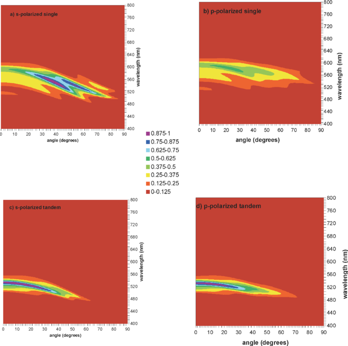 The tandem microcavity device has superior angular emissivity compared to the single microcavity OLED. In both s- and p-polarizations the tandem microcavity OLED displays a peak emission in the normal direction at the wavelength of 520 nm, which remains the peak emission intensity upto viewing angles of ∼30 deg (Figs. 8, 8]. In all cases there is negligible intensity at a large viewing angle. As found in earlier studies20, 21, 22 the strong polarization and angular dependence of the emission is a marked signature of microcavity effects in the OLED, and places constraints on the application of microcavity OLEDs for lighting applications. The emission spectra are also very dependent on the thickness of the emitting layers in the OLED, which needs to be optimized accurately to achieve the brightest OLEDs. 3.ConclusionIn conclusion, both measurements and simulations found blueshifts in the emission between microcavity single unit and tandem OLEDs. The EL spectra narrowed for the microcavity tandem OLEDs relative to the single unit devices. The simulation methods are proved to be consistent with the experimental results and can be considered as a useful tool for directing tandem OLEDs fabrication. We have developed a new scattering matrix method for simulating OLEDs, where Maxwell's equations are solved in Fourier space and the dipoles in the emissive layer represent the sources. This versatile technique has computational advantages and is used to simulate the normal and total emission of the OLED and the angular dependence of the emitted radiation. This technique is a powerful platform for future investigations of white light tandem OLEDs where different emissive layers can be utilized within the tandem structure, and the wavelengths can be combined to provide white light emission with good chromaticity. AcknowledgmentsWe acknowledge very helpful discussions with K. M. Ho and Ames Laboratory Photonics group members. Research at the Ames Laboratory was supported by the Department of Energy, Division of Basic Energy Sciences, under Contract No. DE-AC02–07CH11358. R.B. acknowledges funding from the National Science Foundation through Grant No. ECCS-0601377. ReferencesA. Dodabalapur, L. J. Rothberg, and T. M. Miller,
“Color variation with electroluminescent organic semiconductors in multimode resonant cavities,”
Appl. Phys. Lett., 65 2308
–2310
(1994). http://dx.doi.org/10.1063/1.112726 Google Scholar
T. Shiga, H. Fujikawa, and Y. Taga,
“Design of multiwavelength resonant cavities for white organic light-emitting diodes,”
J. Appl. Phys., 93 19
–22
(2003). http://dx.doi.org/10.1063/1.1527708 Google Scholar
Q. Wang, J. Ding, Z. Zhang, D. Ma, Y. Cheng, L. Wang, and F. Wang,
“A high performance tandem white OLED combining highly effective white-units and their interconnection layer,”
J. Appl. Phys., 105 076101
(2009). http://dx.doi.org/10.1063/1.3106051 Google Scholar
M. Gather, N. M. Kroenberg, and K. Meerholz,
“Monolithic integration of multi-color organic LEDs by grayscale lithography,”
Adv. Mater., 22 4634
–4638
(2010). http://dx.doi.org/10.1002/adma.201002033 Google Scholar
T.-Y. Cho, C.-L. Lin, and C.-C. Wu,
“Microcavity two-unit tandem organic light-emitting devices having a high efficiency,”
Appl. Phys. Lett., 88 111106
(2006). http://dx.doi.org/10.1063/1.2185077 Google Scholar
S. Hamwi, J. Meyer, M. Kroger, T. Winkler, M. Witte, T. Riedl, A. Kahn, and W. Kowalsky,
“The role of transition metal oxides in charge generation layers for stacked organic light emitting diodes,”
Adv. Func. Mater., 20 1762
–1766
(2010). http://dx.doi.org/10.1002/adfm.201000301 Google Scholar
S. Hermann, O. D. Gordan, M. Friedrich, D. R. T. Zahn,
“Optical properties of multilayered Alq3/α-NPD structures investigated with spectroscopic ellipsometry,”
Phys. Status Solidi C, 2 4037
–4042
(2005). http://dx.doi.org/10.1002/pssc.200562211 Google Scholar
J. Frischeisen, D. Yokoyama, C. Adachi, and W. Brütting,
“Determination of molecular dipole orientation in doped fluorescent organic thin films by photoluminescence measurements,”
Appl. Phys. Lett, 96 073302
(2010). http://dx.doi.org/10.1063/1.3309705 Google Scholar
R. Biswas, S. Neginhal, C. G. Ding, I. Puscasu, E. Johnson,
“Mechanisms underlying extraordinary transmission in sub-wavelength hole arrays,”
J. Opt. Soc. of America B, 24 2489
–2495
(2007). Google Scholar
D. Zhou, and R. Biswas,
“Photonic crystal enhanced light-trapping in thin film solar cells,”
J. Appl. Phys., 103 093102
(2008). http://dx.doi.org/10.1063/1.2908212 Google Scholar
Z. Y. Li and L. L. Lin,
“Photonic band structures solved by a plane-wave-based transfer-matrix method,”
Phys. Rev. E., 67 046607
(2003). http://dx.doi.org/10.1103/PhysRevE.67.046607 Google Scholar
L.-L Lin, Z.-Y. Li, and K.-M. Ho,
“Lattice symmetry applied in transfer-matrix methods for photonic crystals,”
J. Appl. Phys., 94 811
–823
(2003). http://dx.doi.org/10.1063/1.1587011 Google Scholar
Handbook of the Optical Constants of Solids II, Academic Press, Boston
(1991). Google Scholar
K. S. Nalwa, and S. Chaudhury,
“Design of light trapping microscale-textured surfaces for efficient organic solar cells,”
Opt. Exp., 18 5168
–5178
(2010). http://dx.doi.org/10.1364/OE.18.005168 Google Scholar
F. Hamelmann, A. Brechling, A. Aschentrup, U. Heinzmann, P. Jutzi, J. Sandrock, U. Siemeling, T. Ivanova, A. Szekeres, and K. Gesheva,
“Thin molybdenum oxide films produced by molybdenum pentacarbonyl 1-methylbutylisonitrile with plasma-assisted chemical vapor deposition,”
Thin Solid Films, 446 167
–171
(2004). http://dx.doi.org/10.1016/j.tsf.2003.09.045 Google Scholar
D. Whittaker and I. Culshaw,
“Scattering-matrix treatment of patterned multilayer photonic structures,”
Phys. Rev. B, 60 2610
–2618
(1999). http://dx.doi.org/10.1103/PhysRevB.60.2610 Google Scholar
H. Rigenault, F. Lemarchand, and A. Sentenac,
“Dipole radiation into grating structures,”
J. Opt. Soc. Am. A, 17 1048
–1058
(2000). http://dx.doi.org/10.1364/JOSAA.17.001048 Google Scholar
S. Nowy, B. Krummacher, J. Frischeisen, N. Reinke, and W. Brutting,
“Light extraction and optical loss mechanisms in OLEDs: Influence of the emitter quantum efficiency,”
J. Appl. Phys., 104 123109
(2008). http://dx.doi.org/10.1063/1.3043800 Google Scholar
R. Biswas, C. G. Ding , I. Puscasu, M. Pralle, M. McNeal, J. Daly, A. Greenwald, and E. Johnson,
“Theory of subwavelength hole arrays coupled with photonic crystals for extraordinary thermal emission,”
Phys. Rev. B., 74 045107
(2006). http://dx.doi.org/10.1103/PhysRevB.74.045107 Google Scholar
N. A. Reinke, C. Ackermann, and W. Bruting,
“Light extraction via leaky modes in OLEDs,”
Opt. Comm., 266 191
–197
(2006). http://dx.doi.org/10.1016/j.optcom.2006.04.081 Google Scholar
M. Flammich, M. C. Gather, N. Danz, D. Michaelis, A. H. Brauer, K. Meerholz, and A. Tunnermann,
“Orientation emissive dipoles in OLEDs: quantitative in situ analysis,”
Org. Electron., 11 1039
–1046
(2010). http://dx.doi.org/10.1016/j.orgel.2010.03.002 Google Scholar
T. Wehlus, T. Körner, S. Nowy, J. Frischeisen, H. Karl, B. Stritzker, and W. Brütting,
“Hybrid organic–inorganic materials for integrated optoelectronic devices,”
Phys. Status Solidi. A, 208 264
–275
(2010). http://dx.doi.org/10.1002/pssa.201026524 Google Scholar
|