|
|
1.IntroductionLighting consumes a significant fraction of the world's total energy budget, and the need for more efficient lighting products has been apparent for a number of years. The replacement of the incandescent light bulb is well underway, however the efficiency of the currently available compact fluorescent bulbs is still lower than is necessary in the long term, and these can also suffer from other issues such as poor color rendering. In addition to achieving high power efficiency with a high color rendering index, it is necessary for any proposed solution to be suitable for large volume low cost manufacture. Polymer organic light-emitting diode (OLED) devices are well suited to this requirement as they use a simple device structure which minimizes the number of deposition steps. An additional advantage is that the materials are well-suited to solution processing which enables efficient material utilization and a reduced number of deposition steps requiring high vacuum, enabling high through-put and a larger substrate area. The ability of OLEDs to claim a part of the lighting market has led to a wealth of research in the area. Many types of devices have been demonstrated, utilizing various combinations of fluorescent and phosphorescent emission. It is not within the scope of this paper to discuss these; readers are referred to a recent review article for further information.1 Previous work at Cambridge Display Technology (CDT) has focused on using a single component white emitting polymer, in which three chromophores of different colors are combined in a single material.2 While the use of two chromophores, carefully chosen so that the combination of their emission gives the perception of white light, is possible, the use of three or more chromophores is preferable as this allows a fuller portion of the spectrum to be filled, thus giving better color reproduction which is important for many lighting applications. This development utilized fluorescent blue and green emitters along with a phosphorescent red emitter which afforded a material with the performance shown in Table 1. This performance was achieved in devices without using optical outcoupling enhancement technology. Table 1Performance of single component white polymer.
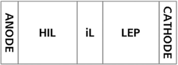
The performance of this material class was ultimately limited by the efficiency of the emitters utilized. In a single-color green device the external quantum efficiency (EQE) of the fluorescent green chromophore was only 5%; thus, replacing this chromophore with a phosphorescent emitter offers significant scope for improvement through the well-known ability of the phosphorescent emitters to utilize both singlet and triplet excitons.3, 4 In parallel with the development of the single component white materials, development of phosphorescent green dendrimer materials had continued within our company, yielding devices with an EQE of 16% in a simple device structure of indium tin oxide (ITO)/spin-coated hole injection layer (HIL)/hole-transporting interlayer/light-emitting polymer (LEP)/low work-function cathode (see Fig. 1). The performance of these two green materials is outlined in Table 2. In order to improve the efficiency of our white devices further, development has focused on combining the efficiency improvements achieved with the phosphorescent green system into our white devices. As discussed above it is also desirable to achieve this in a simple device in order to minimize manufacturing costs. This paper discusses the initial development of a device structure to achieve such an aim. Table 2Comparison of performance of fluorescent and phosphorescent green materials.
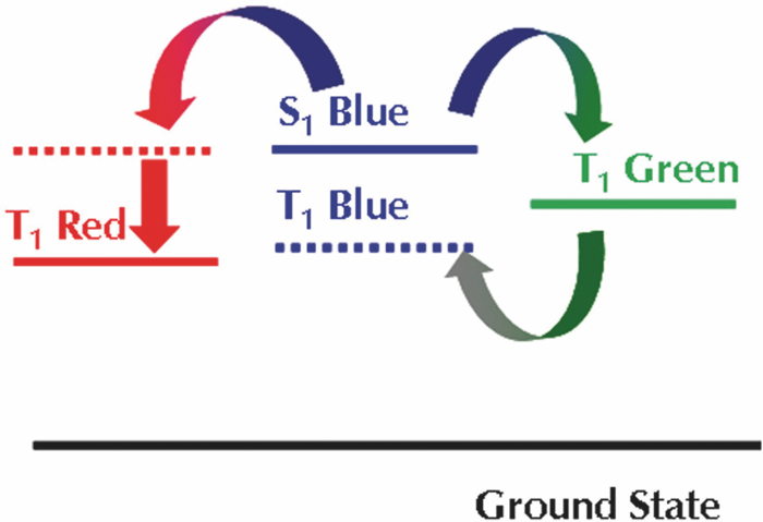
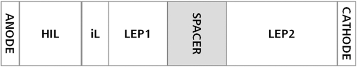
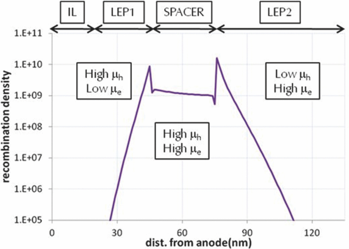
2.Development of Device StructuureFor the previous single component white polymer, the excitons were formed mainly on the blue emitter, with the other chromophores being excited by energy transfer from the blue, as shown in Fig. 2. The introduction of a phosphorescent green emitter is problematic in this regard as the emissive triplet level of the green emitter is higher than the non-emissive triplet level of the fluorescent blue emitter, which leads to quenching of the green emission if the two are in close proximity (see Fig. 3). It is thus necessary to separate the fluorescent blue and phosphorescent green chromophores. Fig. 2Relative energy levels of fluorescent blue and green and phosphorescent red emitters in a single component polymer. 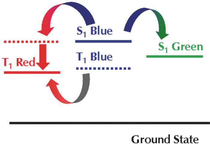 The triplet levels that are discussed in this work have not been directly measured, rather they have been determined relative to one another by assessing whether the materials were able to sustain phosphorescent green emission (T1 level 2.4 eV) or phosphorescent red emission (T1 level 2.0 eV) when blended with an appropriate phosphorescent emitter. 2.1.Electrical modellingThe device structure that was used in this work is shown schematically in Fig. 4. This structure allows the separation of the phosphorescent green and fluorescent blue layers, and introduces a spacer layer to prevent the quenching of excitons between the two chromophores. The major challenge with this structure is the control of the recombination of holes and electrons in such a way as to ensure that there is emission from both of the light-emitting materials. To aid device design we undertook electrical modeling of our proposed structure to gain a qualitative understanding of the material properties required. The drift-diffusion equations were solved self-consistently in 1D in a similar fashion to that outlined by Barker5 and Martin6 The equations reduced to a 2 point boundary value problem for which a variety of standard numerical solver routines exist. A Poole–Frenkel style field dependent mobility and the simple Langevin equation for recombination of polarons were used in the model. Explicit charge trapping was neglected, keeping the model as simple as possible and minimising the number of adjustable fitting parameters. Injection was treated using the Scott–Malliaras modification of Schottky barrier boundary conditions.7 The interface between organic layers was treated using the Arkipov equations for hopping between different Gaussian distributions.8 In general the energy offset between the various layers used in the devices was sufficiently small (<0.3 eV) that the offset has a negligible impact on the performance of the device. The model showed that we can control the buildup of charge carriers at the interface of 2 layers by controlling the contrast in mobilities; going from a high mobility layer to a low causes the carriers to buildup on the low mobility side of the interface. To achieve the desired recombination zone at either side of the spacer layer we require a low hole mobility in LEP2 (causing a buildup of holes) and a low electron mobility in LEP1 (giving an electron buildup), along with high mobilities for both carriers in the spacer layer to minimize the charge buildups and hence recombination in this layer (see Fig. 5). 2.2.Materials and Device FabricationThe development of the device was carried out using a phosphorescent deep-red, a phosphorescent green, and a light blue fluorescent emitter. The color points and efficiencies of these three emitters in a simple device structure of ITO/spin-coated HIL/hole-transporting interlayer/LEP/low work-function cathode is shown in Table 3. Table 3Color points and efficiency data for emitters used in this work.
The HIL was a water-soluble transparent conductive polymer, and was the same throughout all of the devices used in this work. The interlayer was a co-polymer formulated to have a high hole mobility in order to aid hole injection into LEP1, along with groups to allow it to be thermally cross-linked in order to render it insoluble and allow subsequent polymer layers to be deposited on top without intermixing of the two materials. The first LEP was formulated to have a hole mobility significantly higher than the electron mobility in that polymer, and to have a triplet level sufficiently high that it did not quench the phosphorescent green dendrimer. Three further variations of this polymer were synthesized with different levels of hole mobility. The spacer layer was similarly formulated to have a high triplet level, with the mobility of both holes and electrons being high. Two variations on this material were also synthesized to aid in understanding how the relative mobilities of the charges affected the performance of the device. Finally the red and blue polymer was formulated to contain the fluorescent blue emitter and the phosphorescent red in a single material. The hole mobility of this polymer was relatively low compared to the electron mobility. The same polymer was used as LEP2 throughout this work. The changes in the mobilities of these materials were achieved by adjusting the level of hole and electron transporting moiety incorporation within the polymer chain. Since charge transport occurs via a hopping mechanism, the density of carrier sites correlates with the charge-carrier mobility. To allow for comparison between these polymers, the relative abilities of the green polymers to transport holes has been graded on an arbitrary scale of 0 to 10 where zero would contain no hole transporting moieties, and 10 is the highest hole mobility polymer used in this work. In the case of the spacer layers, the relative mobility of holes and electrons is reported. These comparisons are shown in Table 4. Table 4Comparative charge mobilities in materials used in this work.
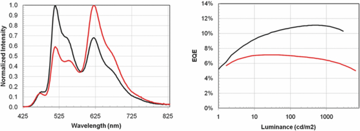
The basic device structure used in the initial investigation is shown earlier in Fig. 4. The transparent conductive HIL was spun on top of a patterned ITO coated glass substrate. The interlayer is formed by spin-coating from o-xylene solution, followed by subsequent baking in a nitrogen atmosphere to effect the cross-linking reaction. Both LEP1 and the spacer layer contained thermally activated cross-linking units, and the layers were formed in analogous fashion to the interlayer. LEP2 did not contain any cross-linking units and was deposited by spin-coating from o-xylene solution but with only a mild thermal drying step to ensure that all solvent was removed. Finally the cathode was thermally evaporated at a pressure of ∼10−6 mbar and consisted of a low work function material capped with aluminum. This method of device manufacture was used for all of the devices described in this study. 4.Three Color White Devices4.1.Prevention of Quenching by the Spacer LayerThe first experiment carried out was to determine whether the spacer layer performed its function of preventing quenching between the green and blue chromophores, while allowing for emission from both layers. These initial devices were fabricated using two polymers, one that contained a phosphorescent green emitter, and the other with fluorescent blue and phosphorescent red. A spacer layer was also synthesized using a formulation that was anticipated to have the properties described above of a high triplet level while also allowing for the transport of both holes and electrons. Two devices were fabricated, device A that did not contain a spacer layer between the green and blue and red polymer, and device B that did contain the spacer layer. The performance of the two devices is shown in Fig. 6. In device A, which had no spacer layer, emission was obtained from all three chromophores, however the maximum EQE was only 7%, with an EQE of 6.5% at a luminance 1000 cd/m2. In comparison device B showed a much stronger green peak, with a maximum EQE of 11%, and an EQE of 10.5% at a luminance of 1000 cd/m2. From these results it was concluded that the device was functioning as intended by design. The spacer layer was preventing quenching between the fluorescent blue and phosphorescent green chromophores, which accounted for the stronger green peak, and it was also transporting both holes and electrons to give the majority of the recombination in the zones to either side of the spacer layer. 4.2.Color Tuning Using the Spacer LayerThe next stage of the investigation was to determine how the properties of the spacer layer could be used to control the color of emission from the device. Details of the materials used in the development of the devices used in this work are in Table 5. Table 5Details of polymer materials used in devices made in this work. The HIL, interlayer, and blue and red polymer (LEP2) were the same in all devices.
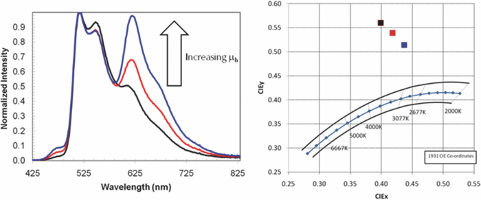
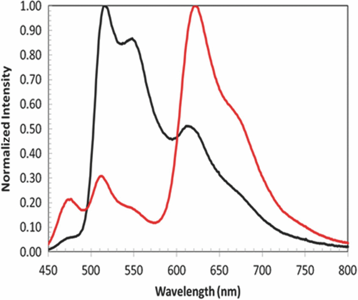
Three devices were fabricated using the same green and red and blue polymers where the properties of the spacer layer were adjusted to vary the relative mobilities of holes and electrons, while keeping the mobilities of both high. See Fig. 7 for the electroluminesence spectra and CIE coordinates for devices 1, 2 and 3. It was found that as the relative mobility of the holes was increased the relative proportion of emission from the layer closest to the cathode increased, i.e., the proportion of emission from the blue and red layer increased relative to the green. 4.3.Color Tuning Using the Charge Mobility in LEP1The relative hole mobility in LEP1 can also be used to tune the proportions of emission from the two emissive layers, in a similar fashion to the tuning that can be achieved by variations in the spacer layer. Changing the green polymer from green 1 in device 1 to green 2 in device 4 caused a significant drop in the proportion of green emission, see Fig. 8. This change in emission color is interpreted in the same way as the changes in emission spectra discussed in Sec. 4.2. The lower hole mobility in the bottom layer when green 1 is used results in a relative buildup of holes in this layer, and so fewer holes pass through the spacer layer into the blue and red polymer. A greater proportion of the recombination thus occurs in the green layer, resulting in an increase in the green emission. 5.Color Tuning to White EmissionAt this point we had demonstrated to our satisfaction that it was possible to build the device, and to tune the color of emission by varying the properties of the materials that we used. The learning described in Secs. 4.1, 4.2, 4.3 was then applied to obtain devices that had emission colors that fell within the specifications for white. Device 3 was taken as a starting point, as this has the emission color that was closest to the white point, although the CIE was too high as a result of the green emission being too strong. Device 3 used green 1 and Spacer 3. To decrease the strength of the green peak the hole mobility in the green polymer was significantly increased (green 1 → green 3), and that in the spacer layer decreased to compensate for the increased hole mobility in the green layer (Spacer 3 → Spacer 1) to give device 5. This resulted in a color point of (0.454, 0.435) just outside the desired area. By increasing the hole transport in the green polymer slightly (green 4) and keeping all other aspects of the device the same it was possible to fine tune the color point, and obtain a point just inside the area defining white emission (device 6). The electroluminesence spectra and CIE coordinates are shown in Fig. 9 and the performance of these devices is summarized in Table 6. Table 6Performance data for devices 7 and 8.
The introduction of the phosphorescent green emitter has enabled an increase in the EQE of the device from 9% in the single component materials using a fluorescent green chromophore to 13.1% in device 6. To obtain a rough estimate of how well the device is functioning, an estimate of the relative contributions of each chromophore to the spectrum was made from the color points of the emitters in single layer devices. This is an approximation as the spectra will be changed slightly in this device structure due to cavity effects. This reveals that the relative contributions from each chromophore are in the approximate ratio of 3:2:1 for red, green, and blue, respectively. The weighted average of the EQEs of each emitter is thus around 13%, which implies that there is minimal quenching in this device, and also a low loss to recombination in the spacer layer. It is likely that recombination does occur to some extent in the spacer layer. However, this layer contains no triplet emitter. Any triplets that are formed are likely to diffuse to the adjacent emissive layers as the triplet level of the spacer is higher than that of both the emitter in LEP1 and LEP2 and triplets tend to be long lived, thus it is only singlets that are formed in the spacer layer that will result in the loss of efficiency. The increase in EQE is also accompanied by an increase in the current efficiency from 14 to 20 cd/A, however there was no increase in the power efficiency due the increased drive voltage in the new structure. Reducing the drive voltage of these devices to obtain the benefits of the increase in current efficiency is the focus of ongoing work. 6.ConclusionsThe device structure that was developed in this work enables the combination of phosphorescent green and fluorescent blue emitters without any significant loss of external quantum efficiency. This was achieved by using electrical modeling to determine the charge transport properties that were required for the materials, and the formulation and synthesis of materials that met these requirements. The color of emission from the device can be tuned by varying the charge transport properties of the materials that are used; this can adjust the relative proportion of recombination from each of the emissive layers. AcknowledgmentsThe authors would like to thank their colleagues in CDT for the preparation of the materials used in this work, and colleagues at both CDT and Sumitomo Chemical Co. for useful discussions. ReferencesK. T. Kamtekar, A. P. Monkman, and M. R. Bryce,
“Recent advances in white organic light-emitting materials and devices (WOLEDs),”
Adv. Mater., 22 572
–582
(2010). http://dx.doi.org/10.1002/adma.200902148 Google Scholar
T. Pounds,
“Developments in Solution Processable Polymers for Lighting,”
Google Scholar
K. A. King, P. J. Spellane, and R. J. Watts,
“Excited-state properties of a triply ortho-metalated iridium(III) complex,”
J. Am. Chem. Soc., 107 1431
–1432
(1985). http://dx.doi.org/10.1021/ja00291a064 Google Scholar
M. A. Baldo, D. F. O’Brien, Y. You, A. Shoustikov, S. Sibley, M. E. Thompson, and S. R. Forrest,
“Highly efficient phosphorescent emission from organic electroluminescent devices,”
Nature (London), 395 151
–152
(1998). http://dx.doi.org/10.1038/25954 Google Scholar
J. A. Barker, C. M. Ramsdale, and N. C. Greenham,
“Modeling the current-voltage characteristics of bilayer polymer photovoltaic devices,”
Phys. Rev. B, 67 075205
(2003). http://dx.doi.org/10.1103/PhysRevB.67.075205 Google Scholar
S. J. Martin, A. B. Walker, A. J. Campbell, and D. D. C. Bradley,
“Electrical transport characteristics of single-layer organic devices from theory and experiment,”
J. Appl. Phys., 98 063709
(2005). http://dx.doi.org/10.1063/1.2058199 Google Scholar
J. C. Scott,
“Metal–organic interface and charge injection in organic electronic devices,”
J. Vac. Sci. Technol. A, 21 521
–531
(2003). http://dx.doi.org/10.1116/1.1559919 Google Scholar
V. I. Arkhipov, E. V. Emelianova, and H. Bassler,
“Charge carrier transport and recombination at the interface between disordered organic dielectrics,”
J. Appl. Phys., 90 2352
–2357
(2001). http://dx.doi.org/10.1063/1.1388566 Google Scholar
|