
|
|
1.IntroductionThe discovery of electroluminescence (EL) from π-conjugated semiconductors stimulated great interest in these materials.1, 2 The brightness, efficiency, and lifetime of organic light-emitting diodes (OLEDs) have improved dramatically, leading to commercial applications in displays3 and potential for solid state lighting.4 Optimized carrier injection from the electrodes into the organic layers is a fundamental requirement for high efficiency OLEDs, particularly for devices that incorporate materials with large energy gaps. Carrier injection in OLEDs is generally optimized by matching the work function of the anode with the highest occupied molecular orbital (HOMO) level of the hole transport material and that of the cathode with the lowest unoccupied molecular orbital (LUMO) level of the electron transport material. Within a device structure, its properties will be governed by an interplay between the electric field F and the properties of the constituent materials. Indium tin oxide (ITO) has been the preferred anode material in opto-electronics, because it combines good optical transparency (>90% in the visible) with reasonably low resistance (<100 Ω/square). The relatively low work function of ITO (4.5 to 5 eV) combined with interface dipoles at the ITO/organic interface, however, results in barriers to hole injection. Hole injection from an ITO anode has been enhanced by incorporating a hole injection layer (HIL) between ITO and the organic layer(s). A variety of materials have been used to facilitate hole injection from ITO, e.g., copper phthalocyanine,5, 6 metal oxides,7, 8 and conducting polymers.9, 10 A blend of polyethylene dioxythiophene and polystyrene sulfonate (PEDOT:PSS) is a popular hole injection material in both organic light-emitting diodes and solar cells. The work function of PEDOT:PSS is about 5.1 ± 0.1 eV,11, 12 which is significantly higher than that of ITO. Brown et al.13 have shown that incorporation of PEDOT:PSS substantially increases the built-in potential (Vbi) in polymer light-emitting diodes(LEDs), implying reduced barriers to hold injection. However, PEDOT-PSS is strongly acidic14 and PSS has been shown to etch ITO. This results in the incorporation of indium into the active layer of the device and leading to serious concerns about the device lifetime and reliability.15 These issues have driven the development of polymer HILs16, 17 with higher work functions and less acidity to give improved device performance and stability. Choudhury et al. studied small molecule OLEDs with a HIL based on a conducting polymer polythienothiophene (PTT) doped with poly(perfluoroethyleneperfluoroethersulfonic acid) (PFFSA) in OLEDs.18 Hole only devices with 4,4′-bis[N-1-napthyl-N-phenyl-amino]biphenyl (α-NPD) or N,N′-diphenyl-N,N′-bis(3-methylphenyl)-1,10-biphenyl-4,40-diamine showed significantly higher currents for devices with PTT:PFFSA HILs as opposed to PEDOT:PSS or CuPc. Bi-layer OLEDs with PTT:PFFSA polymer formulations applied as the HIL were found to have reduced operating voltages, higher brightness and significantly longer lifetimes. Continued development of polymer HILs should benefit from a better understanding of OLEDs incorporating these materials. A number of studies of polymer-based OLEDs have shown that the efficiency of hole injection from PEDOT:PSS is enhanced by electron injection. Murata concluded that a build-up of electrons at the anode increases the electric field at this electrode and enhances hole injection.19 The injected current density and EL intensity of PPV-based LEDs studied by van Woudenbergh far exceeded predictions, leading the authors to suggest that trapped electrons at the anode alter the electric field distribution and enhance hole injection.20 Lane showed21 that incorporation of a PEDOT:PSS HIL increases the built-in potential by 0.7 V, much greater than can be accounted for the difference in the work function between ITO and PEDOT:PSS. This effect was attributed to electron trapping at the HIL/polyfluorene interface. These effects are not limited to heavily doped hole injection layers. Morgado22 obtained a substantial increase in device efficiency by inserting a blocking layer of poly(1,4-phenylene vinylene) layer between PEDOT:PSS and the emissive layer, a blend of poly(9,9-dialkyl-fluorene-2,7-diyl) and poly(9,9-dioctylfluorene-alt-benzothiadiazole). They likewise concluded that electron accumulation at the interface with the hole injection layer assists carrier injection. Although electron accumulation at the HIL interface plays an important role in polymer LEDs, structural differences between vacuum-deposited and solution-processed OLEDs make this unlikely. Small molecule-based OLEDs typically have discrete layers for hole transport, electron transport, and emission, whereas a polymer OLED generally has a composite layer combining all three functions. Electron injection is blocked at the interface between the hole transport and emissive layers, leading to a vanishingly low electron density at the interface between the hole injection and transport layers and making electron trapping unlikely. Accumulation of charge at interfaces that exist within a multilayer structure will have a profound influence on the electric field distribution. These structural differences warrant an investigation of this type of device structure. We focus on how incorporation of a HIL affects the internal electric field distribution within the multilayer structure. Electroabsorption (EA) spectroscopy has been widely used to study organic optoelectronic devices, including light-emitting diodes and solar cells.13, 21, 23, 24, 25, 26, 27, 28, 29, 30 This technique relies upon a change in absorption in response to an electric field. The field causes a Stark shift of energy levels, resulting in an EA spectrum proportional to the square of the electric field and the imaginary part of the third order dc Kerr nonlinear susceptibility, χ(3)(–ω;0,0,ω).31 To the lowest order and for a material without a permanent dipole moment in its ground state or lowest excited state, the EA spectrum of a material will follow the first derivative of the absorption spectrum with respect to energy. For an unoriented material with a difference in the dipole moment in the ground and excited states, the EA spectrum will follow the second derivative of the absorption spectrum with respect to energy. In a typical EA experiment, sinusoidally varying reference bias is superimposed upon the dc bias (Vdc), producing a time-dependent bias of the form: [TeX:] \documentclass[12pt]{minimal}\begin{document}\begin{equation}
V\left( t \right) = V_{{\rm dc}} + V_{{\rm ref}} \sin \Omega t,
\end{equation}\end{document} where Ω is the modulation frequency in rad/sec. Absent carrier injection, the dc field Edc and the dc bias are related by Edc = (Vdc–Vbi)/d d is the width of the device. For a device so biased:
[TeX:] \documentclass[12pt]{minimal}\begin{document}\begin{equation}
- \frac{{\Delta T}}{T} \propto \left( {2E_{{\rm dc}} E_{{\rm ac}} \sin \Omega t + {\textstyle{1 \over 2}}E_{{\rm ac}} ^2 \cos 2\Omega t} \right){\mathop{\rm Im}\nolimits} \chi ^{\left( 3 \right)}
\end{equation}\end{document} where ΔT is the change in probe transmission, T. The EA signal, measured with a lock-in amplifier referenced to the modulation frequency, varies linearly with Vdc. The most common use of EA spectroscopy of devices has been to measure Vbi which should coincide with the zero-level crossing of the EA signal.Campbell et al.23 pioneered the use of EA spectroscopy in polymer LEDs, demonstrating that the maximum Vbi is limited by the energies of the electron and hole transport levels. Later uses of EA spectroscopy on polymer LEDs include the effect of interlayers between the anode13, 21, 25 on Vbi, the field distribution in polymer light-emitting electrochemical cells,26 and device degradation.27 Although EA spectroscopy has been used primarily to study polymer OLEDs, there have been two studies of bi-layer OLEDs that with an α-NPD hole transport layer and a tris(quinolin-8-olato) aluminum (III) (Alq3) electron transport and emission layer. Rohlfing et al.29 concluded that the average electric fields in the α-NPD and the Alq3 layers are similar in reverse bias but the field in the Alq3 layer is considerably larger than that in the α-NPD layer in forward bias. These effect were attribute to hole accumulation at the α-NPD/Alq3 interface. Martin et al.30 later performed EA measurements of similar structures and also modeled the field and carrier densities. Hole accumulation at the α-NPD/Alq3 interface was found to suppress the field in the hole transport layer, but the ratio was closer to 2:1 at +4 V forward bias. The electron density in the hole transport layer was found to be negligible, suggesting that electron trapping effects found in polymer OLEDs19, 20, 22 will not be seen in bi-layer cells. 2.Experimental MethodDevices were fabricated by spin-coating a 30-nm layer of PTT:PSSFA onto a substrate that had been pre-patterned with ITO. Layers of α-NPD and Alq3 were successively deposited under vacuum at a pressure of 3 × 10⁻⁶ Torr, followed by a cathode consisting of 10 Å of LiF capped by 100 nm of aluminum. The devices were encapsulated in dry nitrogen and measured at room temperature under ambient conditions. The operational characteristics of similar devices have previously been described.18 In our electromodulation (EM) spectrometer, light from a quartz halogen lamp is dispersed through a 150-mm monochromator (Acton Research) and focused onto the active area of the LED through a semi-transparent electrode, typically the anode. Most groups have used a reflection geometry in which the cathode acts as a mirror and light is transmitted through the organic layers twice. After exiting the device, light is focused onto a photoreceiver and field-dependent changes in transmission are detected by lock-in amplification. Our experimental set-up uses a silicon photodiode (OSI Optoelectronics) coupled to a matched transimpedance preamplifier (Judson Technologies PA-7) with a gain of 105 V/A and a 10-kHz bandwidth. A differential amplifier was used to provide a dc bias upon which a sinusoidally varying reference bias (Vref) is superimposed. One issue that arises when measuring OLEDs is that modulated electroluminescence can be orders of magnitude greater than the modulated transmission. This effect can be compensated for by using two photoreceivers: Detector A is positioned at the focus of the probe beam and detector B is positioned so as to detect the same modulated EL signal as detector A. The lock-in amplifier accepts two inputs, locking in on the difference signal between the two photoreceivers. We refer to this as balanced mode operation. One cannot completely eliminate modulated EL from the signal in this way as the photoreceivers are slightly out of phase from one another as measured by the lock-in amplifier. This is presumably due to differences in the photodiode capacitance or the preamp transfer function or both. The residual modulated EL adds a slight baseline to the quadrature spectrum that was subtracted before normalization. Modulation of the probe beam can also occur from excited state absorption of carriers, a particular trapped charge, or neutral excitations such as triplet excitons that form upon recombination.32 Structural relaxation occurs in a π-conjugated molecule upon oxidation, reduction, or excitation. For example, in linear phenylenevinylene molecules, the phenylene moiety changes from an aromatic configuration to a partially quinoidal one. What were the HOMO and LUMO levels, one of which is now partially occupied, shift into the gap and new transitions appear slightly below the gap and in the infrared. Excited state absorption will also be accompanied by bleaching of the HOMO – LUMO transition. We use the term electromodulation for any change in absorption and reserve the term electroabsorption for changes in probe transmission related to nonlinear optical properties. 3.Results and Discussion3.1.Electromodulation MeasurementsFigure 1 shows the EM spectrum of a single layer Alq3 with the structure ITO/(100 nm)Alq3/Al. The dc bias was −2 V and the reference amplitude was 200 mV rms. The spectrum is normalized to the sample transmission and closely approximates the change in optical density due to the electric field. The experimental data are shown as symbols and the solid line was calculated from a multi-Gaussian fit to the experimental data before normalization. The spectrum shows a classic oscillatory behavior with a maxima at λ = 450 nm. For the purposes of this work, the intensity of the EA signal is proportional to the average electric field in the Alq3 layer. The EA signal had a linear dependence on the applied bias with a zero level crossing at 2.8 V, the built-in potential (Vbi). This is much higher that that expected from the work function difference between ITO (5 eV) and aluminum (4.1), indicating the presence of interface dipoles and/or significant chemistry at the ITO/Alq3 and Alq3/Al interfaces.33 This was primarily a test structure to identify the position of the EA peak of Alq3. The EA spectrum of a single layer α-NPD device is shown in Fig. 1 for comparison.29 This work was performed by Rohlfing on a device with a 100 nm thick layer of α-NPD and under a field of 21 kV/cm. The EA spectrum of α-NPD has a maxima at λ = 410 nm and does not contribute for λ > 450 nm. Fig. 1EM spectrum of (a) ITO/(100 nm)Alq3/Al (F = X kV/cm) and (b) ITO/(100 nm)a-NPD/Al devices (F = 21 kV/cm). Symbols show the experimental data in (a) and the line shows a multi-Gaussian fit to ΔT. The data for Fig. 1 was measured by Rohlfing (Ref. 24). 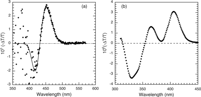 Figure 2 shows the EM spectrum of a bi-layer device with a polymer HIL, measured with the dc bias set to –0.7 V and the reference amplitude to 0.5 V rms. The spectrum has a maxima at λ = 460 nm and minima at λ ≈ 400 nm and λ = 520 nm. The maxima is attributed to EA of Alq3 as it matches the peak in the single layer Alq3 device. The minima at λ ≈ 400 nm lies at a point where there is a minima from Alq3 as well as a maxima from α-NPD, assuming that the electric field has the same polarity in both layers. In devices measured by Martin, contributions from α-NPD were the dominant feature at this wavelength, resulting in a maxima at 400 nm rather than a minima.30 This was largely due to the EA signal of α-NPD being 8 times larger than that of Alq3. In contrast, the ratio of these two peaks measured here [Figs. 1, 2] is fairly similar for both structures, roughly 4:3. This would suggest that even in reverse bias, the electric field strength in the α-NPD layer is roughly an order of magnitude weaker than that in the Alq3 layer; an effect that can only be attributed to the incorporation of an HIL. The minima at λ = 520 nm was observed by neither Rohlfing29 nor Martin30 and thus is a direct consequence of incorporation of a hole injection layer. Fig. 2EM spectrum of an ITO/HIL/(40 nm)α-NPD/(40 nm)Alq3/LiF/Al device, measured at –0.7 V dc bias and with a 0.5 V rms reference bias modulated at 1 kHz. In-phase: filled symbols. Quadrature: open symbols. The line is shown as a guide for the eye. 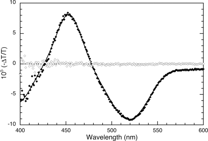 Figure 3 shows the dependence of the Alq3 signal, measured at a fixed wavelength of 460 nm as the dc bias was swept from –5 to +2 V with a reference bias amplitude of 0.5 V rms. The signal depends linearly upon the applied bias between – and –1 V and then abruptly changes slope. The zero-level crossing occurs at 0.3 V forward bias and the signal increases magnitude, reaching a maximum negative amplitude at ∼2 V forward bias. This behavior lies in sharp contrast to that of the single layer device or bi-layer devices previously studied.22, 24 The change in slope of Alq3 EA was correlated with an increase in the intensity of the EM band, shown in Figure 4. The greater sample transmission below the optical gap permitted a lower reference bias, 0.2 V rms. The excited state absorption ESA signal is roughly independent of the dc bias up to 0.2 V reverse bias and then sharply increases, reaching a maximum value at 3 V forward bias. In addition to a sharp increase in the magnitude of the EM signal at 0 V, there is also a slight phase shift as can be seen by a non-zero quadrature signal. Fig. 3Dependence of the (a) Alq3 EA signal (λ = 460 nm) and (b) EM signal (λ = 520 nm) on the applied bias. The reference voltage was 0.2 V rms, modulated at 1 kHz for both measurements. 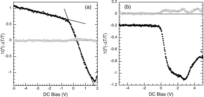 Fig. 4EM spectra of the bi-layer OLED measured at (a) 1.7 V dc bias with a reference bias of 0.5 V rms and (b) 3 V dc bias with a reference bias of 200 mV rms. The reference bias was modulated at 1 kHz for both scans In-phase: filled symbols. Quadrature: open symbols. The line is shown as a guide for the eyes for the near-UV portion of the spectrum. 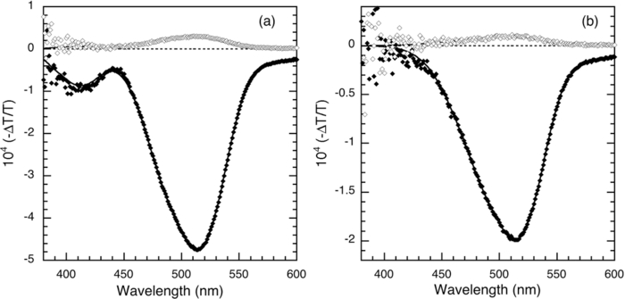 The correlation between the Alq3 EA signal and the EM band is made clear by the EM spectra of the OLED in forward bias both above and below the turn-on voltage (2.5 V). Figure 4 shows the EM spectrum of the device at a dc bias of 1.7 V, where the EM signal is changing most rapidly with the dc bias, and at a dc bias of 3 V, at its maximum value. A larger reference bias could be used for the spectrum at 1.7 V as the bias dependence is linear between 1 and 3 V. This permitted a better signal-to-noise ratio to be obtained in the portions of the spectrum where the spectrometer throughput was weak (< 450 nm). The measurement above the turn-on voltage was performed in balanced mode and the lock-in phase was set to that of the EL to eliminate any phase shifts associated with the electrical circuit. Both spectra are dominated by the EM band as one might anticipate by the sharp increase in the bias sweeps. Unlike the spectrum measured in reverse bias, there is a slight shift in the phase of the signal, resulting in a non-zero quadrature signal with the same lineshape as that of the in-phase signal and much weaker amplitude. 3.2.Field-Modulated Excited State AbsorptionWe consider the origin of the EM band with a minima at λ = 520 nm. This feature cannot arise from EA of the transport layers as it lies beyond the cut-off wavelength (see Fig. 1) nor can it originate from EA of the hole injection layer as it cannot support a strong internal electric field. We note that this signal was detected below the turn-on voltage and thus neutral species such as singlet and triplet excitons are precluded. Furthermore, it was not detected in studies of bi-layer α-NPD/Alq3 OLEDs without the HIL.29, 30 These observations lead us to focus on the HIL/α-NPD interface as the origin of this feature with the possibility that the HIL may be partially oxidizing the α-NPD layer. Upon removing a charge from a π-conjugated molecule, structural relaxation shifts the LUMO and what was the HOMO into the gap.32 Adding charge to a π-conjugated molecule results in similar relaxation. In consequence, induced absorption bands form a below the absorption edge and in the infrared arise and these could account for a subgap EM signal. There are three possibilities which could account for the EM band: α-NPD cations, Alq3 anions, or charges in the HIL. We consider each in turn. Alq3 has previously been observed to react with the cathode or an electron injection layer such as LiF. Choong studied the interface between calcium and Alq3 by ultraviolet photoemission spectroscopy.37 Doping-induced absorption was seen between 0.8 and 2.0 eV (λ > 600 nm) and the maxima of subgap absorption occurs at 720 nm. The EM band lies at a significantly shorter wavelength and therefore cannot originate from Alq3 anions. Jiang measured the absorption spectrum of PTT:PFFSA and showed that the absorption peak from doped states occurs at around 1500 nm.35 Furthermore, the absorption cut-off of the HIL lies below 500 nm and therefore this feature cannot be related to de-doping of the HIL. We are therefore left with the possibility that the field modulation of α-NPD cations could be the source of the EM band. In order to prove this assignment, we measured changes in the absorption spectrum of α-NPD following oxidation by FeCl3, a Lewis acid. Solution of α-NPD and FeCl3 in chloroform were prepared at a concentration of 0.017 M (10 mg/ml for α-NPD). Figure 5 shows the absorption spectra as the α-NPD solution was progressively doped by addition of FeCl3 (roughly 5% addition by volume each). An optical transition with a maxima around 480 to 500 nm appears immediately upon addition of FeCl3 and strengthens with increasing amounts of FeCl3. A second lower-energy transition is seen in the long wavelength portion of these spectra. The lineshape of the doping induced absorption spectrum was independent of the dopant concentration and we did not observe a second oxidation step due to dication formation. Figure 5 compares the EM band with doping-induced changes in α-NPD absorption. The EM band occurs at a slightly longer wavelength than solution doping, due to solvatochromic effects. These results are consistent with those observed by Endo, who studied co-evaporated films of α-NPD and FeCl3.36 Given the close resemblance between the EM band and α-NPD+ absorption and the dissimilarities with charged species of Alq3 and PTT:PFFSA, we therefore conclude that this band is due to ESA by field-modulated α-NPD cations. Fig. 5(a) Absorption spectrum of a 17 mM α-NPD solution as it is progressively doped by FeCl3. Inset: a Jablonski diagram of the optical transitions of α-NPD and α-NPD+. (b) Dashed line: doping-induced absorption spectrum of α-NPD. Solid line: difference between the EA spectrum of a single layer Alq3 device and that of the bi-layer device with a PTT:PFFSA hole injection layer. 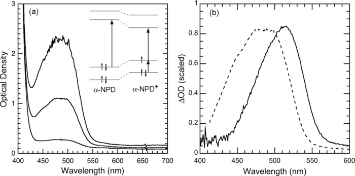 Further insight into the nature of the species responsible for ESA is obtained by considering its sign, phase, and amplitude. For EA of a device, increased absorption occurs when the reference electric field has the same polarity as the dc field. For a device in reverse bias with respect to the built-in potential, the internal field is greatest when sin Ωt < 0. The ESA has the opposite sign as that of the EA signal and therefore follows the absolute polarity of the reference field, not its polarity relative to the built-in potential. Thus, the density of α-NPD cations increases with increasing positive bias and is independent of the polarity of the dc field. We next consider whether the ESA signal is due to injected carriers or trapped charge. These species can be distinguished by the dependence of the signal upon the modulation frequency. The dependence of the ESA signal on modulation frequency and excitation lifetime is given by: [TeX:] \documentclass[12pt]{minimal}\begin{document}\begin{equation}
\Delta T_X \propto {1 / {[ {1 + ( {\Omega \tau } )^2 }]}},
\end{equation}\end{document}
[TeX:] \documentclass[12pt]{minimal}\begin{document}\begin{equation}
\Delta T_Q \propto {{\Omega \tau } / {[ {1 + ( {\Omega \tau } )^2 } ]}},
\end{equation}\end{document} where τ is the excitation lifetime, ΔTX is measured with the lock-in set-in phase with the modulation, and ΔTQ is measured with the lock-in set 90° out of phase with the modulation (quadrature). The transit time for mobile charge carriers across the α-NPD layer is of order tens of nanoseconds, assuming a bias of order 1 V and previously measured mobility (5 × 10⁻⁴ cm2/V).37 Any signal associated with mobile carriers will therefore follow the electric field modulation, resulting in a signal with amplitude and phase independent of the modulation frequency below 1 MHz. We see a clear phase shift between the electric field and the ESA signal in the spectra measured at 1.7 and 3 V (Fig. 4), resulting in a non-zero quadrature signal. The ratio between the in-phase to quadrature signal is 15:1 for the spectrum measured at 1.7 V and 20:1 for the spectrum measured at 3 V, corresponding to an excitation lifetime ∼10 μs. We conclude that the EM signal originates from field modulation of trapped charge at the HIL/α-NPD interface.The doping-induced and electromodulation spectra permit us to calculate the magnitude of field-dependent doping. The transmitted probe light I(d) through the sample is given by: [TeX:] \documentclass[12pt]{minimal}\begin{document}\begin{equation}
I\left( d \right) = I_0 \left( {1 - R} \right)e^{ - \alpha d},
\end{equation}\end{document} where I0 is intensity of the probe light incident on the film, α is the absorption coefficient, d is the film thickness, R is the reflectivity, and reflections from the backside of the film are neglected. It has been shown that ΔR/R < 10−6 for organic semiconductors31 and thus changes in reflectance can be neglected in the case of the much stronger electromodulation seen here. Taking into account that the absorption coefficient is equal to the product of the excitation density (n) and the absorption cross section (σ), we arrive at the final relation:
[TeX:] \documentclass[12pt]{minimal}\begin{document}\begin{equation}
- \frac{{\Delta T}}{T} = \Delta n\sigma d.
\end{equation}\end{document} The absorption cross section for α-NPD+ can be calculated from the doping induced absorption spectrum (Fig. 5). The absorption cross section of a molecule is given by:
[TeX:] \documentclass[12pt]{minimal}\begin{document}\begin{eqnarray}
\sigma = 1000\ln 10\frac{\varepsilon }{{N_A }},
\end{eqnarray}\vskip-6pt\end{document} where ɛ is the molar extinction coefficient and NA is Avogadro's number. A peak optical density of 0.82 was obtained by 5% doping of a 0.017 M solution and a 0.2 cm path length. Assuming 100% oxidation of α-NPD, we calculate an extinction coefficient of ɛ = 4700 cm−1 M−1 and a corresponding cross section σ = 1.8 × 10⁻¹⁷ cm2. Using the data from Fig. 4, an EM signal of 2 × 10⁻⁴ was obtained for a dc bias of 3 V and a reference bias 0.2 V rm. The change in the surface excitation density of Δnd ≈ 1013 cm−2 (∼1 μC/cm2). This is equivalent to 1% doping of a 10-nm thick layer of α-NPD (or 10% doping of a 1-nm thick layer).2.3.Internal Electric Field DistributionWe finally consider the effect of the HIL on the electric field distribution within the device and attempt to determine the built-in potential (Vbi). The calculation of Vbi in our devices is complicated by field-dependent modulation of the trapped charge density at the α-NPD/HIL interface as well as overlap of the EA spectrum of Alq3 and the ESA spectrum of α-NPD+. Bodrozic previously considered how to determine Vbi in devices with one of several different polyfluorene derivatives as the active layer and an ITO/PEDOT:PSS anode. Careful analysis of the dependence of the EA signal upon wavelength, frequency, and applied bias enabled an accurate determination of Vbi. It was important to measure the bias-dependence of the EA peak at high frequency (Ωτ ≪ 1) where the frequency dependence of the ESA minimizes its contribution [see Eqs. 3, 4]. The ESA signal in this device is considerably stronger relative to the EA signal seen in studies of polymer LEDs.28 For example, the EA signal of poly(9,9-dioctyl-fluorene-alt-N-(4-butylphenyl)-diphenylamine) was 2 orders of magnitude larger than that of the ESA signal. Hence, the ESA signal was a moderate perturbation that was amenable to analysis. The ESA signal in forward bias is roughly an order of magnitude stronger than the EA signal in the spectra of our device. We first consider how field-modulated doping of α-NPD impacts the bias response of the EA signal. Consider the bias dependence of the EA signal shown in Fig. 3. The EA signal is linear with dc bias when the device is in reverse bias, but the slope is much weaker than one might expect. The extrapolated zero-level crossing occurs at 7.0 V, an unphysical built-in potential. Couple this observation with the relatively weak electric field in the α-NPD layer in comparison to that observed by Rohlfing29 and Martin30 and it becomes evident that the HIL is doing more than simply assisting injection of holes. At roughly zero dc bias, there is a sharp increase in the magnitude of the ESA signal and a concommitant increase in the slope of the EA signal. The zero-level crossing occurs at 0.3 V forward bias, well below the expected built-in potential, and is indicative of a sharply reduced field strength in the Alq3 layer as well as overlap between the Alq3 EA and α-NPD+ ESA spectra. Couple these observations with the relatively weak electric field in the α-NPD layer in comparison to that observed by Rohlfing29 and Martin30 and it becomes evident that the HIL is doing more than simply assisting injection of holes. Rather, the electric field appears to be concentrated in the Alq3 layer for a device in reverse bias and the field distribution dramatically changes in forward bias. Although the forward bias EM spectra are dominated by the α-NPD+ band, there are slight differences between the two spectra that are due to electroabsorption and allow us to infer the built-in potential. Figure 6 compares the two spectra, scaled to the α-NPD+ minima at 520 nm. There is a clear oscillatory deviation between the two spectra below 480 nm. This difference, shown in Fig. 6, approximates the EA portion of the spectrum shown in Fig. 1. It is difficult to pinpoint the exact built-in potential as the EA signal of Alq3 for V > Vbi will be negative and difficult to differentiate from the much stronger negative signal of the α-NPD+ ESA band. It is clear that the spectrum measured with Vdc = 1.7 V lies below the built-in potential as the EA peak is still positive and rides on top of the negative ESA band of α-NPD+. The difference spectra gives a peak magnitude of [TeX:] ${{ - \Delta T} \mathord{\left/ {\vphantom {{ - \Delta T} T}} \right. \kern-\nulldelimiterspace} T} = 2 \times 10^{ - 5}$. Given the EA response of Alq3 [see Fig. 1], this corresponds to a potential difference of roughly 0.5 V and a built-in potential of 2.3 ± 0.1 V. Fig. 6(a) EM spectra of the bi-layer OLED from Fig. 5, scaled to the maxima of the α-NPD+ peak. Filled symbols: measured with 1.7 V dc bias. Open symbols: measured with 3 V dc bias. (b) The difference spectrum between these two EM spectra. 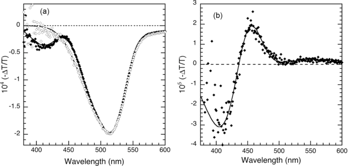 The observation of modulated charge injection into α-NPD has significant implications for device operation. We observed a suppression of the electric field in the α-NPD layer in reverse bias, possibly due to accumulation of holes at the α-NPD/Alq3 interface would concentrate the electric field in the Alq3 layer. Small molecule OLEDs have been produced on similar principles, using a doped layer of the hole transport material for enhanced hole injection. Endo used a composite α-NPD:FeCl3 layer to enhance hole injection in bi-layer OLEDs.34 Leo and co-workers have demonstrated highly efficient phosphorescent OLEDs using doped hole transport and electron transport layers. One potential limitation of this approach is that ions can migrate through the organic layer, reducing device efficiency and lifetime. Our results suggest that a polymer HIL has a similar effect with the added advantage that doping is field dependent rather than on a concentration gradient and proceeds on a time scale of order microseconds. 4.Summary and ConclusionsIn conclusion, we have studied bi-layer α-NPD/Alq3 OLEDs with a polymer hole injection layer by electromodulation spectroscopy. The HIL substantially modifies the electric field distribution within the device due to field-dependent doping of the α-NPD hole transport layer. In reverse bias, this has the effect of suppressing the field strength within the α-NPD layer and concentrating it in the Alq3 layer. In forward bias, the electromodulation spectrum is dominated by field-dependent modulation of α-NPD cations. The modulated surface charge density is of order 1013 cm−2 (∼μC/cm2), equivalent to a 1% change in doping for 0.2 V rms (0.5 V peak-to-peak). The built-in potential is estimated to be between 2.2 and 2.5 V, which is consistent with low injection barriers to electrons and holes. ReferencesC. W. Tang, S. A. VanSlyke, and C. H. Chen,
“Electroluminescence of doped organic films,”
J. Appl. Phys., 65
(9), 3610
–3616
(1989). http://dx.doi.org/10.1063/1.343409 Google Scholar
J. H. Burroughes, D. D. C. Bradley, A. R. Brown, R. N. Marks, K. MacKay, R. H. Friend, P. L. Burn, and A. B. Holmes,
“LEDs based on conjugated polymers,”
Nature (London), 347
(6293), 539
–541
(1990). http://dx.doi.org/10.1038/347539a0 Google Scholar
A. R. Duggal, D. F. Foust, W. F. Nealon, and C. M. Heller,
“Fault-tolerant, scalable organic light-emitting device architecture,”
Appl. Phys. Lett., 82
(16), 2580
–2582
(2003). http://dx.doi.org/10.1063/1.1569653 Google Scholar
S. A. Van Slyke, C. H. Chen, and C. W. Tang,
“Organic electroluminescent devices with improved stability,”
Appl. Phys. Lett., 69
(15), 2160
–2162
(1996). http://dx.doi.org/10.1063/1.117151 Google Scholar
F. Nüesch, D. Berner, E. Tutis, M. Schaer, C. Ma, X. Wang, B. Zhang, and L. Zuppiroli,
“Doping-induced charge trapping in organic light-emitting devices,”
Adv. Funct. Mater., 15
(2), 323
–330
(2005). http://dx.doi.org/10.1002/adfm.200305022 Google Scholar
J. Li, M. Yahiro, K. Ishida, H. Yamada, and L. Matsushige,
“Enhanced performance of organic light emitting device by insertion of conducting/insulating WO3 anodic buffer layer,”
Synth. Met., 151
(2), 141
–146
(2005). http://dx.doi.org/10.1016/j.synthmet.2005.03.019 Google Scholar
H. You, Y. F. Dai, Z. Q. Zhang, and D. Q. Ma,
“Improved performances of organic light-emitting diodes with metal oxide as anode buffer,”
J. Appl. Phys., 101
(2), 026105
(2007). http://dx.doi.org/10.1063/1.2430511 Google Scholar
S. A. Carter, M. Angelopoulos, S. Karg, P. J. Brock, and J. C. Scott,
“Polymeric anodes for improved polymer light-emitting diode performance,”
Appl. Phys. Lett., 70
(16), 2067
–2069
(1997). http://dx.doi.org/10.1063/1.118953 Google Scholar
Y. Cao, G. Yu, C. Zhang, R. Menon, and A. J. Heeger,
“Polymer light-emitting diodes with polyethylene dioxythiophenepolystyrene sulfonate as the transparent anode,”
Synth. Met., 87
(2), 171
–174
(1997). http://dx.doi.org/10.1016/S0379-6779(97)03823-X Google Scholar
A. J. Mäkinen, I. G. Hill, R. Shashidhar, N. Nikolov, and Z. H. Kafafi,
“Hole injection barriers at polymer anode/small molecule interfaces,”
Appl. Phys. Lett., 79
(5), 557
–559
(2001). http://dx.doi.org/10.1063/1.1386400 Google Scholar
N. Koch, A. Elschner, J. Schwartz, R. L. Johnson, and A. Kahn,
“Organic molecular films on gold versus conducting polymer: Influence of injection barrier height and morphology on current–voltage characteristic,”
Appl. Phys. Lett., 82
(14), 2281
–2283
(2003). http://dx.doi.org/10.1063/1.1565506 Google Scholar
T. M. Brown, J. S. Kim, R. H. Friend, F. Cacialli, R. Daik, and W. J. Feast,
“Built-in field electroabsorption spectroscopy of polymer light-emitting diodes incorporating a doped poly(3,4-ethylene dioxythiophene) hole injection layer,”
Appl. Phys. Lett., 75
(12), 1679
–1681
(1999). http://dx.doi.org/10.1063/1.124789 Google Scholar
H. Kim, J. Park, S. Lee, C.-S. Ha, and Y. Kim,
“Effect of strong base addition to hole-collecting buffer layer in polymer solar cells,”
Sol. Energy Mater. Sol. Cells, 95
(1), 349
–351
(2011). http://dx.doi.org/10.1016/j.solmat.2010.04.023 Google Scholar
S. A. Choulis, V.-E. Choong, M. K. Mathai, and F. So,
“The effect of interfacial layer on the performance of organic light-emitting diodes,”
Appl. Phys. Lett., 87
(11), 113503
(2005). http://dx.doi.org/10.1063/1.2042635 Google Scholar
D. W. Laird, S. Vaidya, S. Li, M. Mathai, B. Woodworth, E. Sheina, S. Williams, and T. Hammond,
“Advances in Plexcore™ active layer technology systems for organic photovoltaics: Roof-top and accelerated lifetime analysis of high performance organic photovoltaic cells,”
Proc. SPIE, 6656 66560X
(2007). http://dx.doi.org/10.1117/12.734711 Google Scholar
X. Jiang, H. Yan, E. H. Klingenberg, and D. L. Elder,
“Enhanced lifetime of polymer light-emitting diodes using poly(thieno[3,4-b]thiophene)-based conductive polymers,”
Proc. SPIE, 6333 633304
(2006). http://dx.doi.org/10.1117/12.682742 Google Scholar
K. R. Choudhury, J. Lee, N. Chopra, A. Gupta, X. Jiang, F. Amy, and F. So,
“Highly efficient hole injection using polymeric anode materials for small-molecule organic light-emitting diodes,”
Adv. Funct. Mater., 19
(3), 491
–496
(2009). http://dx.doi.org/10.1002/adfm.200801368 Google Scholar
K. Murata, S. Cina, and N. C. Greenham,
“Barriers to electron extraction in polymer light-emitting diodes,”
Appl. Phys. Lett., 79
(8), 1193
–1195
(2001). http://dx.doi.org/10.1063/1.1396627 Google Scholar
T. van Woudenbergh, P. W. M. Blom, and J. N. Huiberts,
“Electro-optical properties of a polymer light-emitting diode with an injection-limited hole contact,”
Appl. Phys. Lett., 82
(6), 985
–987
(2003). http://dx.doi.org/10.1063/1.1543255 Google Scholar
P. A. Lane, P. J. Brewer, J. Huang, D. D. C. Bradley, and J. C. de Mello,
“Elimination of hole injection barriers by conducting polymer anodes in polyfluorene light-emitting diodes,”
Phys. Rev. B, 74
(12), 125320
(2006). http://dx.doi.org/10.1103/PhysRevB.74.125320 Google Scholar
J. Morgado, R. H. Friend, and F. Cacialli,
“Improved efficiency of light-emitting diodes based on polyfluorene blends upon insertion of a poly(p-phenylene vinylene) electron-confinement layer,”
Appl. Phys. Lett., 80
(14), 2436
–2438
(2002). http://dx.doi.org/10.1063/1.1467981 Google Scholar
I. H. Campbell, T. W. Hagler, D. L. Smith, and J. P. Ferraris,
“Direct measurement of conjugated polymer electronic excitation energies using metal/polymer/metal structures,”
Phys. Rev. Lett., 76
(11), 1900
–1903
(1996). http://dx.doi.org/10.1103/PhysRevLett.76.1900 Google Scholar
I. H. Campbell, D. L. Smith, C. J. Neef, and J. P. Ferraris,
“Optical properties of single carrier polymer diodes under high electrical injection,”
Appl. Phys. Lett., 78
(3), 270
–272
(2001). http://dx.doi.org/10.1063/1.1340859 Google Scholar
T. M. Brown, R. H. Friend, I. S. Millard, D. J. Lacey, T. Butler, J. H. Burroughes, and F. Cacialli,
“Electronic line-up in light-emitting diodes with alkali-halide metal cathodes,”
J. Appl. Phys., 93
(10), 6159
–6172
(2003). http://dx.doi.org/10.1063/1.1562739 Google Scholar
J. C. deMello, J. J. M. Halls, S. C. Graham, N. Tessler, and R. H. Friend,
“Electric field distribution in polymer light-emitting electrochemical cells,”
Phys. Rev. Lett., 82
(2), 421
–424
(2000). http://dx.doi.org/10.1103/PhysRevLett.85.421 Google Scholar
C. Giebeler, S. A. Whitelegg, D. G. Lidzey, P. A. Lane, and D. D. C. Bradley,
“Device degradation of polymer light emitting diodes studied by electroabsorption measurements,”
Appl. Phys. Lett., 75
(14), 2144
–2146
(1999). http://dx.doi.org/10.1063/1.124944 Google Scholar
P. A. Lane, J. C. de Mello, R. B. Fletcher, and M. Bernius,
“Electric field screening by injected charge in polymer light-emitting diodes,”
Appl. Phys. Lett., 83
(17), 3611
–3613
(2003). http://dx.doi.org/10.1063/1.1623014 Google Scholar
F. Rohlfing, T. Yamada, and T. Tsutsui,
“Electroabsorption spectroscopy on tris-8-hydroxyquinoline–aluminum-based light emitting diodes,”
J. Appl. Phys., 86
(9), 4978
–4984
(1999). http://dx.doi.org/10.1063/1.371469 Google Scholar
S. J. Martin, G. L. B. Verschoor, M. A. Webster, and A. B. Walker,
“The internal electric field distribution in bilayer organic light emitting devices,”
Org. Electron., 3
(3–4), 129
–141
(2003). http://dx.doi.org/10.1016/S1566-1199(02)00050-2 Google Scholar
L. Sebastian and G. Weiser,
“One-dimensional wide energy-bands in a polydiacetylene revealed by electroreflectance,”
Phys. Rev. Lett., 46
(17), 1156
–1159
(1981). http://dx.doi.org/10.1103/PhysRevLett.46.1156 Google Scholar
P. Shakya, P. Desai, R. J. Curry, and W. P. Gillin,
“Improved electron injection into Alq3 based devices using a thin Erq3 injection layer,”
J. Phys. D: Appl. Phys., 41
(8), 085108
(2008). http://dx.doi.org/10.1088/0022-3727/41/8/085108 Google Scholar
P. A. Lane, X. Wei, and Z. V. Vardeny,
“Studies of charged excitations in π-conjugated oligomers and polymers by optical modulation,”
Phys. Rev. Lett., 77
(8), 1544
–1547
(1996). http://dx.doi.org/10.1103/PhysRevLett.77.1544 Google Scholar
J. Endo, T. Matsumoto, and J. Kido,
“Organic electroluminescent devices with a vacuum-deposited Lewis-acid-doped hole-injecting layer,”
Jpn. J. Appl. Phys., 41
(3B), L358
–L360
(2002). http://dx.doi.org/10.1143/JJAP.41.L358 Google Scholar
V.-E. Choong, M. G. Mason, C. W. Tang, and Y. Gao,
“Investigation of the interface formation between calcium and tris-(8-hydroxy quinoline) aluminum,”
Appl. Phys. Lett., 72
(21), 2689
(1998). http://dx.doi.org/10.1063/1.121100 Google Scholar
X. Jiang, K. Campbell, F. Amy, B. Han, F. So, K. R. Choudhury, and A. Gupta,
“Tuning the properties of polythienothiophene conductive polymers for hole injection layer application,”
SPIE Proc., 6655 665505
(2007). http://dx.doi.org/10.1117/12.768007 Google Scholar
S. Naka, H. Okada, H. Onnagawa, Y. Yamaguchi, and T. Tsutsui,
“Carrier transport properties of organic materials for EL device operation,”
Synth. Met., 111–112 331
–333
(2000). http://dx.doi.org/10.1016/S0379-6779(99)00358-6 Google Scholar
|


