|
|
1.IntroductionWith increasing world wide energy consumption of which roughly 20% are used for lighting, high efficiency, white organic light emitting diodes (OLEDs) recently became a potential alternative for conventional incandescent light bulbs. Therefore, the research on white OLEDs has gained more importance during the last years.1, 2 These usually consist of several functionalized layers such as charge injection and transport layers for holes and electrons and up to three different emission layers, one for each primary color. To obtain diodes with high power efficiencies one has to have an efficient current-to-light conversion as well as a low driving voltage. The voltage can be reduced by electrically doping the charge transport layers with electron donors or acceptors.3 In different publications it was shown that halides such as FeCl3 (Ref. 4), metal oxides like WO3 (Ref. 5), and organic molecules like F4TCNQ (Ref. 6) can act as electron acceptors and metals with low work function like Cs (Ref. 7), organometallic molecules like cobaltocene,8 as electron donors. This increases the conductivity of the layers and improves the injection of charge carriers from adjacent electrodes. In this manuscript we show the doping of transport layers by the use of two cheap (important for mass production purposes), nearly colorless doping materials, namely rhenium heptoxide (Re2O7) for p-doping and cesium carbonate (Cs2CO3) for n-doping. 2.Doping MechanismDoped transport layers usually are fabricated by a co-evaporation of a transport material and a lowly concentrated dopant. In the case of p-doping, the dopants which are embedded within the host material have to have a LUMO level in the range of the host's HOMO. This leads to a charge-transfer complex as an electron is transferred from the host's HOMO to the LUMO of the dopant. If the distance between the two charges is large enough, the coulombic interaction becomes sufficiently small so that the hole remaining on the host molecule is free to move to other molecules. A schematic of the process is shown in Fig. 1. This process increases the density of free holes and therefore also the conductivity of the layer. The relation is given by Eq. 1 with p and p0 being the free hole density and free intrinsic hole density (very low for most organic materials), NA the dopant (acceptor) density and γ the probability of an ionization process. The conductivity σ of the sample is described by Eq. 2. Here, e is the unit charge, μ is the hole mobility, and p is the free hole density. Similar equations are used to describe the n-doping process. Fig. 1Depiction of p-doping mechanism. (a) An electron from the host's HOMO level is transferred to the LUMO of the dopant via a charge-transfer complex. (b) The hole which remains on the host's HOMO can now freely move within the layer. 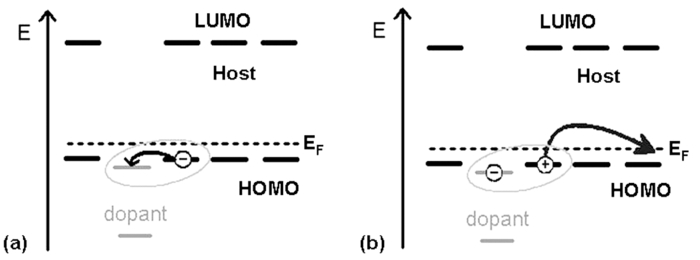 [TeX:] \documentclass[12pt]{minimal}\begin{document}\begin{equation}
p = p_0 + N_A \cdot \gamma,
\end{equation}\end{document} The charge-transfer complex which enables the generation of additional free charges in the doped layers also has optical effects which can be important for optoelectronic devices. Even if both materials, the host as well as the dopant, individually produce colorless layers, the charge-transfer complex causes so-called charge-transfer states which can absorb light in the visible region. Thus, the use of colorless dopants can help to minimize the absorption of the doped layer but nevertheless it will absorb more as the doping concentration increases. 3.Increased Conductivity in Single Layer DevicesTo investigate the increased conductivity of our p- and n-doped transport layers, simple single layer devices consisting of a 150-nm organic layer between indium tin oxide (ITO) and aluminum (Al) electrodes have been fabricated. The host and dopant molecules for the organic layer are N,N′-di-1-naphtyl-N,N′-diphenyl-4,4′-diamino-biphenyl (α-NPD) and rhenium heptoxide (Re2O7) for p-doping and 4,7-diphenyl-1,10-phenanthroline (BCP) and cesium carbonate (Cs2CO3) for n-doping. Figure 2 presents a schematic of the two different material sets with the HOMO and LUMO values for the undoped matrices α-NPD and BCP between the two electrodes. The concentrations of both dopants are chosen to be 1%, 10% and 50% to investigate doping effects over a wide range. Fig. 2Device layouts and molecular structures for conductivity measurements on p- and n-doped transport layers. Φ is the work function of the electrode material. (a) p-doping of hole-transport material with Re2O7 and (b) n-doping with Cs2CO3. 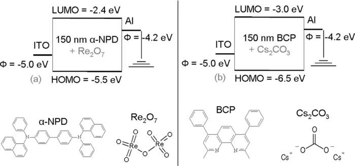 Figure 3 shows the current density vs. voltage plots (IV curves) of these devices. It can be seen that the IV characteristics of the p- and n-doped layers show increasing currents with higher doping concentrations as more free charge carriers are generated. But the increased charge carrier densities not only affect the conductivity of the material but also the injection of charge carriers from the electrodes. Since α-NPD is a better hole than electron conductor, the current in the p-doped samples is strongly dominated by holes. These are either injected from the ITO for positive or from the aluminum for negative voltages. The injection becomes easier with higher doping concentrations which results in increasing currents and more symmetrical IV curves. This effect will be discussed in Sec. 4. In the double logarithmic plot of the IV curves in Fig. 3 an ohmic behavior can be seen for voltages below 0.2 V. In this region the current is not yet affected by a changing injection and therefore allows investigation of the layer's conductivity. It can be calculated from the IV's slope in the ohmic region using Ohm's law [Eq. 3]. [TeX:] \documentclass[12pt]{minimal}\begin{document}\begin{equation}
j = \sigma \cdot E = \sigma \cdot \frac{U}{d}.
\end{equation}\end{document} Here j is the current density, E is the electrical field, U is the voltage, and d is the organic layer thickness. Identical calculations can be done for the case of n-doping. Here, positive and negative voltages result in an electron dominated current from the aluminum or the ITO, respectively. Table 1 shows conductivities of the different p- and n-doped samples. The pure layers of α-NPD and BCP have a low conductivity of roughly 10−14 S/cm which can be strongly increased by a moderate doping concentration of 10% of Re2O7 and Cs2CO3, respectively. p-doped layers gained 8 and n-doped ones at least 6 orders of magnitude in conductivity. Since the conductivity of undoped organic layers is much lower than the doped ones, additional doped transport layers are not going to increase a device's driving voltage. This is discussed in Sec. 5.Table 1Conductivity values obtained from the ohmic regions of IV curves in Fig. 3 [using Eq. 3].
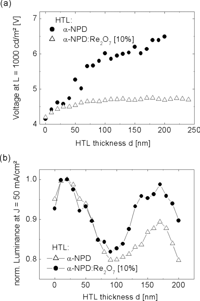
Fig. 3IV curves of the samples shown in Fig. 2. (a) p-doped layers consisting of α-NPD and Re2O7 and (b) n-doped layers consisting of BCP and Cs2CO3. 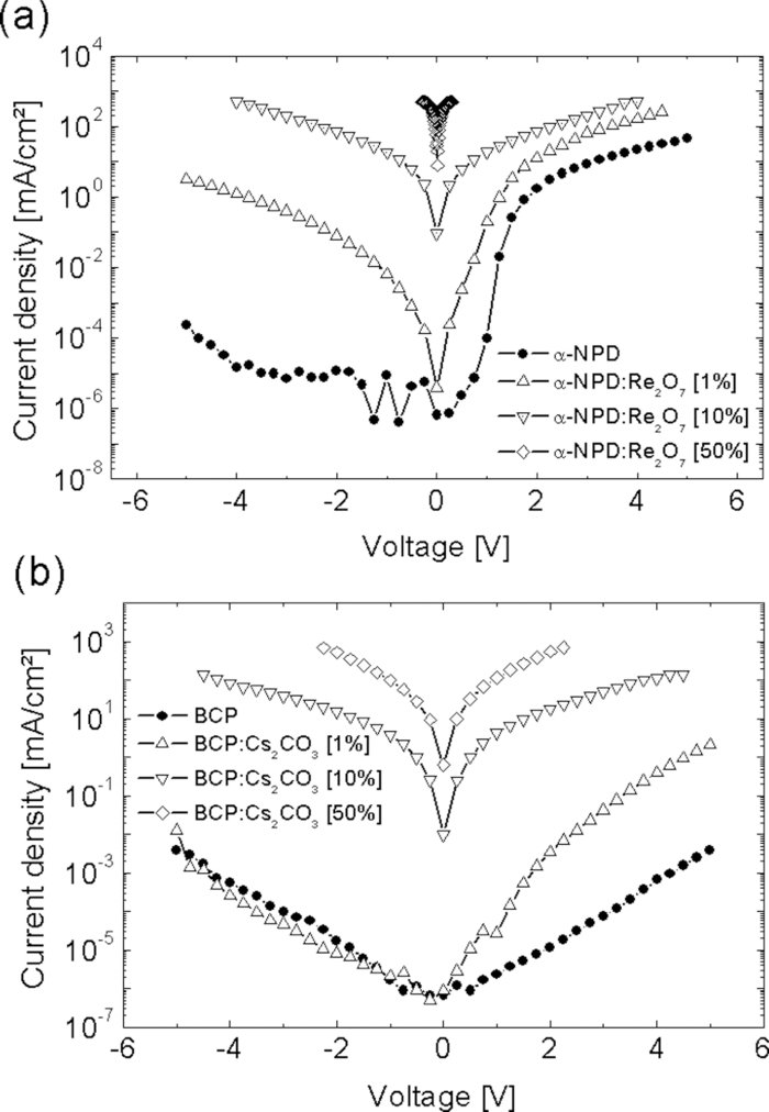 4.Improved Charge Carrier Injection in Multilayer DevicesAs already mentioned in Sec. 3, the increased free charge carrier density in the organic layer can affect the charge carrier injection from adjacent electrodes. In undoped systems, the Schottky barrier which is formed at such an interface usually limits the current flow at higher driving voltages. In this intrinsic case, the charges need additional energy or have to tunnel a long distance to pass the barrier. If the organic layers are doped, the HOMO and LUMO levels close to the interface are bent so that the barrier becomes much thinner. This allows the charge carriers to be injected more easily via thermionic field emission [REFERENZ]. This makes the injection for higher doping concentrations nearly independent of the work function of the electrode, resulting in symmetric IV curves (c.f. Fig. 2). To characterize the injection improvement by doping the transport layers with Re2O7 and Cs2CO3, another four samples for each material set have been prepared. These are called i, p-i, i-p, and p-i-p for p-doping and i, n-i, i-n, and n-i-n for n-doping. In the case of p-doping these consist of the following two types of layers: 150 nm of intrinsic α-NPD and 150 nm of α-NPD doped with 10% Re2O7 which are going to be denoted as i (intrinsic) and p (p-doped), respectively. These two types of layers are arranged in different ways between an ITO and aluminum electrode. The sequences are p-i for a sample with a doped layer next to the ITO and an intrinsic one next to the aluminum, i-p for the reversed case, p-i-p for a sample with p-doped layers on each side, and an intrinsic one in the middle, and i for a sample with just one intrinsic layer. Due to the higher conductivity of the doped layers, the devices’ driving voltages are mostly applied to the intrinsic layers. This creates the same conditions for charge transport in every device. With these four devices, the hole injection improvement from ITO and aluminum into the organics can be measured independently. Similar layouts have been fabricated for n-doping with 150 nm BCP (i) and 150 nm BCP doped with 10% Cs2CO3 (n). The IV curves of the four devices each for p- and n-doping are shown in Fig. 4. Fig. 4IV curves of the devices fabricated to investigate charge injection improvement. p, i, and n denote the kinds of layers used in the sequences shown in the right lower corner. On the left of each sequence is ITO, on the right is aluminum. (a) p-doping with intrinsic α-NPD and α-NPD doped with 10% Re2O7 and (b) n-doping with intrinsic BCP and BCP doped with 10% Cs2CO3.  For the case of p-doping, the i and p-i devices show typical diode behavior. Voltages above 0.9 V for i and 1.2 V for p-i let the current densities increase exponentially as more holes are injected from the ITO. In the i case this is just the energy difference between the work functions of the electrodes while in the p-i case it can be interpreted as the difference between the HOMO of the α-NPD and the work function of the aluminum as the holes reach the intrinsic layer already on this energy level. If the p-doped layer is put next to the aluminum electrode, negative voltages can now also inject holes from the aluminum over the large energy barrier of ΔE ≈ 1.3 eV. Thus, the IV curves become nearly symmetrical and prove that Re2O7 is able to efficiently inject holes into the undoped organics even from a metal with such a low work function. Equivalent behavior can be seen in the case of n-doping. Without doping there is hardly any current running through the device, regardless of the polarity [device i in Fig. 4]. An n-doped layer next to the aluminum or the ITO allows electron injection from these electrodes for positive or negative voltages, respectively (device i-n and n-i). The turn-on voltages, again, can be interpreted as the energy differences between the LUMO of BCP and the work function of the injecting electrode. For the n-i sample they are around 1 V and for the i-n sample around 2 V. For Cs2CO3 doped layers on both sides (n-i-n), the IV curves are symmetrical as electrons can be injected efficiently from either of the electrodes. This shows that the cheap doping materials Re2O7 and Cs2CO3 are well suited to improve charge carrier injection and allow the use of nearly any electrode material regardless of its work function. It also makes the p-i-p and n-i-n structures well suited to investigate the transport properties (mobility via space charge limited current) of intrinsic materials since injection effects are negligible. Diffusion processes of dopant molecules into the intrinsic layers can be excluded because results from impedance spectroscopy did show no differences in capacitance between the four samples, even after being heated to 80°C for 1 h. 5.Variation of HTL Thickness in Alpha-NPD/ALQ3 OLEDsAfter the investigation of the doping mechanism in single layer and multilayer single carrier devices, the p-doped transport layers are now applied to OLEDs. A simple α-NPD/Alq3 device is chosen, in which Alq3 is the electron transporting layer as well as the green emitter. The cathode consists of 0.7 nm LiF and 200-nm aluminum. The layer structure of this simple OLED is shown in Fig. 5. The HTL consists either of pure α-NPD or of 10% rhenium heptoxide doped into α-NPD and is varied between 0 and 200 nm in steps of 10 nm in both cases. With these devices the voltage drop over the p-doped and undoped HTL with increasing layer thickness can be compared. Fig. 5The layer structure of the OLED devices which consists of HTL/10 nm α-NPD/40 nm Alq3 with a variation of the HTL thickness from 0 to 200 nm is shown. As electron injecting contact a 0.7 nm thick LiF layer is used, which is illustrated as the thin gray bar between the Alq3 emitter layer and the aluminum layer. 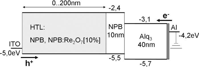 The IV curves of the two kinds of OLEDs show a clear difference for undoped (Fig. 6) and p-doped (Fig. 6) devices. For the undoped samples, the voltage needed to run a constant current density through the device rises linearly with increasing α-NPD layer thickness [Fig. 7]. To reach, for example, a current density of 50 mA/cm2 in the device with 200 nm α-NPD an additional 2.7 V compared to the case with 0 nm α-NPD have to be applied (4.2 V for 0 nm and 6.9 V for 200 nm). Fig. 6IV curves of the OLED devices fabricated to investigate the voltage drop over increasing intrinsic (α-NPD) and doped (α-NPD doped with 10% Re2O7) HTL thickness. The layer structure is shown in Fig. 5. (a) HTL variation from 0 to 200 nm of α-NPD and (b) HTL variation from 0 to 200 nm of α-NPD doped with 10% Re2O7. 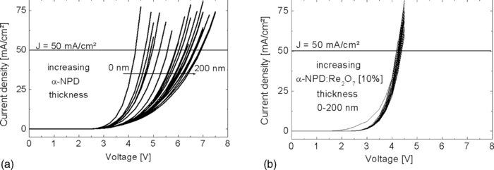 Fig. 7(a) Voltage versus HTL thickness to reach a current density of 50 mA/cm2 in OLEDs with undoped and p-doped HTL. (b) Voltage increase versus current density for devices with undoped and p-doped HTL. 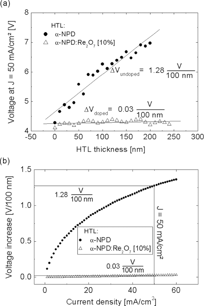 For the 21 OLED devices with p-doped transport layers the IV curves are nearly unchanged. With an HTL consisting of α-NPD doped with 10% Re2O7 one needs a voltage of 4.17 V for devices with 0 nm and 4.22 V for ones with 200 nm thick HTL to be able to reach 50 mA/cm2. Thus, the voltage rise with increasing HTL thickness is very small compared to the undoped OLEDs. The highest voltage (4.39 V) which is needed to reach 50 mA/cm2 has to be applied for a layer thickness of 120 nm. The cause of this irregularity can be explained by the error margin of process fluctuations. In order to be able to quantify the voltage drop over the HTL thickness more accurately, the average voltage rise per 100 nm is determined for current densities from 1 to 60 mA/cm2 [Fig. 7]. As an example, the voltage rise for a current density of 50 mA/cm2 is indicated. It can be seen that it is significantly smaller for the p-doped OLEDs (ΔV = 0.03 ± 0.02 V/100 nm) than for the undoped ones (ΔV = 1.28 ± 0.08 V/100 nm). The average voltage drop over the undoped α-NPD layer of the OLEDs depends strongly on the current density, shown in Fig. 7. While for the undoped OLEDs the voltage increases with higher current density the voltage drop over the p-doped HTL is nearly independent from the current density. This is the reason why the IV curves spread out so much for the undoped OLED samples (Fig. 6). The luminance-voltage (LV) curves of the two types of OLEDs also show a clear difference for undoped and p-doped devices, which are similar to IV curves plotted in Fig. 6. In [Fig. 8] the voltage rise with increasing HTL thickness is shown for the doped and the undoped samples at a constant luminance value of 1000 cd/m2. Due to fact that the current density is proportional to the luminance the IV and the LV curves behave very similarly [cf. Figs. 7 and 8]. The only difference here arises by light out-coupling effects in thin film devices and a higher reabsorption by the increased layer thickness. This increased reabsorption is for the doped layers much stronger compared to the undoped ones, which can be seen by plotting the normalized luminance over the HTL thickness for a constant current density [Fig. 8]. This curve allows the analysis of the influence of the out-coupling in these thin film devices. After a first out-coupling maximum at 30 nm HTL thickness a second maximum at ∼170 nm can be found. 6.ConclusionIn summary, we have shown that the two cheap and nearly colorless doping materials Re2O7 and Cs2CO3 have excellent doping properties. They strongly increase the free charge carrier densities in doped transport layers and also improve the charge carrier injection from adjacent electrodes. Even electrode materials with a large work function mismatch to the organics’ molecular orbitals can be used to efficiently inject charges. These two advantages result in transport layers which cause nearly no additional voltage drop regardless of their thickness as long as undoped organic layers with much higher resistances are used in the same device. In practice, these layers can be used to either investigate the transport properties of materials sandwiched between two doped layers or to tune the microcavity in organic optoelectronic devices. ReferencesJ. Kido, K. Hongawa, K. Okuyama, and K. Nagai,
“White lightemitting organic electroluminescent devices using the poly(Nvinylcarbazole) emitter layer doped with three fluorescent dyes,”
Appl. Phys. Lett., 64
(7), 815
–817
(1994). http://dx.doi.org/10.1063/1.111023 Google Scholar
O. Weiss, R. Krause, and P. Paetzold, Advances in Solid State Physics, 46 321
–332 Springer-Verlag, Heidelberg
(2007). Google Scholar
K. Walzer, B. Maennig, M. Pfeiffer, and K. Leo,
“Highly efficient organic devices based on electrically doped transport layers,”
Chem. Review, 107
(4), 1233
–1271
(2007). http://dx.doi.org/10.1021/cr050156n Google Scholar
M. Fukushima, Y. Hamada, E. Tabei, M. Aramata, S. Mori, and Y. Yasushi,
“Effects of dopants and polymer structures on electrical conductivity of organosilicon polymers,”
Synth. Metals, 94
(3), 299
–306
(1998). http://dx.doi.org/10.1016/S0379-6779(98)00025-3 Google Scholar
M.-T. Hsieh, C.-C. Chang, J.-F. Chen, and C. H. Chen,
“Study of hole concentration of 1,4-bis[N-(1-naphthyl)-N′-phenylamino]-4,4′ diamine doped with tungsten oxide by admittance spectroscopy,”
Appl. Phys. Lett., 89
(10), 103510
(2006). http://dx.doi.org/10.1063/1.2345610 Google Scholar
J. Blochwitz, M. Pfeiffer, T. Fritz, and K. Leo,
“Low voltage organic light emitting diodes featuring doped phthalocyanine as hole transport material,”
Appl. Phys. Lett., 73
(6), 729
–731
(1998). http://dx.doi.org/10.1063/1.121982 Google Scholar
J. Kido and T. Matsumoto,
“Bright organic electroluminescent devices having a metal-doped electron-injecting layer,”
Appl. Phys. Lett., 73
(20), 2866
–2868
(1998). http://dx.doi.org/10.1063/1.122612 Google Scholar
C. K. Chan, F. Amy, Q. Zhang, S. Barlow, S. R. Marder, and A. Kahn,
“N-type doping of an electron-transport material by controlled gas-phase incorporation of cobaltocene,”
Chem. Phys. Lett., 431 67
–71
(2006). http://dx.doi.org/10.1016/j.cplett.2006.09.034 Google Scholar
|
||||||||||||||||||||||||