|
|
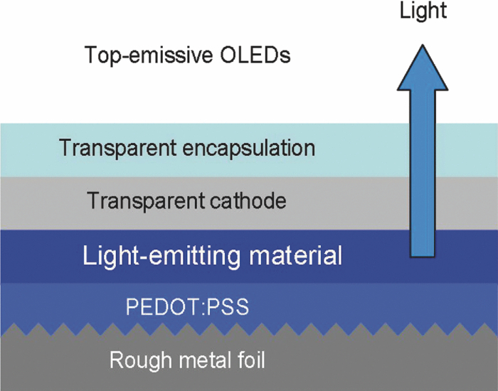
1.Introduction1.1.Top-Emissive OLEDs on Metal FoilThe use of flexible plastic or metal foil substrates allows the advantages of organic electronics to be fully exploited and opens up new application areas and production methods compared to typical glass-based devices. The thin, light weight foils offer flexibility, while still being robust, and are compatible with low-cost roll-to-roll processing. Using metal foil as the flexible substrate for organic light-emitting diodes (OLEDs) is an interesting alternative to plastics such as polyethylene terephthalate (PET) and polyethylene naphthalate (PEN), and offers advantages such as acting as a barrier to oxygen and water on one side of the device and allowing high temperature processing steps and improved dimensional stability.1, 2 Due to the reactive nature of the cathode materials used for most OLEDs, it is more convenient if the metal foil substrate is on the anode side of the device. In this case, a noninverted top-emissive structure is required, with light emission occurring through a semitransparent cathode as shown in Fig. 1.3, 4, 5 The OLED structure can either be made in direct electrical contact with the metal foil or with an insulating planarization layer in between the device and the substrate.6 When the OLED structure makes direct contact to the metal foil it has the advantage that the foil can act as a support electrode for the anode so that no additional conductive layers are needed on this side. A major disadvantage of metal foils is that due to the rolling process for manufacturing an rms roughness of up to hundreds of nanometers is seen. This puts limitations on their direct use, without extra processes such as polishing or planarization, which add to the cost of producing organic electronic devices on these substrates. In the case of such a top-emitting OLED structure, the cathode should have a high reflectivity, a high transparency, and a high conductivity and, in the case of OLEDs without doped layers, a work function that enables efficient charge injection into the adjacent organic layer. In recent years there have been many reports of glass-based top-emissive OLEDs with good performance where Ag,7, 8 Al/Ag,9, 10 LiF/Al12 and LiF/Al/Ag12, 13, 14, 15, 16 have been applied as the transparent cathode, often in combination with a capping layer such as N,N’-bis(naphthalen-1-yl)-N,N’-bis(phenyl)-benzidine (NPB),10, 11, 12, 13, 14, 15, 16, 17 N,N,N’,N’-tetrakis(4-methoxyphenyl)benzidine (MeO-TPD),9 tris(8-hydroxyquinolinato)aluminium (AlQ3)3,17, 18 tin-doped indium oxide (ITO), SiO2,15 or ZnSe.16, 19 With this second metal electrode, a microcavity resonator is obtained that amplifies a specific wavelength range and particular emission angles15, 20, 21 (acting like a Fabry–Pérot filter). As a result, spectral narrowing and an increased angle dependence of the electroluminescence are obtained, which are hard to optimize simultaneously.22 1.2.Optical Microcavity Effects in OLEDsThe work described in this paper is for polymer-based OLEDs, and in such devices light is only generated in a small region of the 80-nm thick light-emitting polymer (LEP) layer which, in the case of top-emissive OLEDs, is between two mirrors, one of which is semitransparent as shown schematically in Fig. 2. As a result the light is reflected multiple times resulting in multiple beam interference and wide angle interference. Fig. 2Diagram showing propagation of light inside and outside of a top-emissive OLED with microcavity effects where n0–n4 are the refractive indices of different layers. 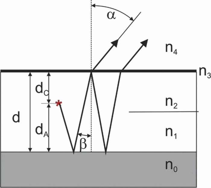 Using the Fabry–Pérot principle23 it can be determined that for a wave with amplitude A0 traveling in all directions within a microcavity the intensity, I, of the light that escapes out of the top of the cavity compared to the intensity, I0, of the light within the cavity is given by [TeX:] \documentclass[12pt]{minimal}\begin{document}\begin{equation}
\frac{I}{{I_0 }} = \left| {\frac{A}{{A_0 }}} \right|^2 = \left| {\frac{{\tau + \rho _A\cdot e^{i\delta _A } }}{{1 - \rho _A \rho _c\cdot e^{i\delta } }}} \right|^2 = \frac{{T_c + R_A + 2\sqrt {R_A T_C } \cos \delta _A }}{{1 + R_A R_C - 2\sqrt {R_A R_C } \cos \delta }}
\end{equation}\end{document} where τ and Tc are the cathode transmission coefficient and absolute transmission respectively, ρc and ρA are the reflection coefficients, and RC and RA are the absolute reflectivities of the cathode and anode. The relationships between the coefficients and absolute values are ρ2 = R and τ2 = T, while
[TeX:] \documentclass[12pt]{minimal}\begin{document}\begin{equation}
\delta = \varphi _A + \varphi _C = \frac{{4\pi nd}}{\lambda }\cdot\cos \beta,
\end{equation}\end{document}
[TeX:] \documentclass[12pt]{minimal}\begin{document}\begin{equation}
\delta _A = \varphi _A + \frac{{2\pi n(d + d_A - d_C)}}{\lambda }\cdot\cos \beta
\end{equation}\end{document} where the phase shifts at the anode and cathode φA and φC are determined by the differences in the complex refractive indices of the PEDOT:PSS and the anode material, and the LEP and the cathode material, respectively. Changing either of the materials will thus influence the optical thickness n·d. The viewing angle is also incorporated, where β is the internal angle (as shown in Fig. 2) and is related to the external viewing angle α by Snell's law n4 sin(α) = n2 sin(β). Equation 1 is essentially the same as those published by Neyts20 and Peng.24From this model it can be seen that the optical distance between the mirrors, i.e., the refractive indices and thicknesses of PEDOT and LEP, and the phase shifts at the reflectors, caused by the change in complex refractive index and thus by the materials that are used for the anode and cathode, will determine the resonance wavelength for the microcavity. In order to characterize the microcavity in real OLED devices the reflectivity spectrum can be used,23 since at the resonance wavelength of the multiple beam interference a dip in the reflectivity will occur. 1.3.Optimizing Top-Emissive OLEDs on Metal FoilIn this paper, with the aim of optimizing the performance of polymer-based, blue top-emitting OLEDs on flexible metal foil substrates, we will show how, by adjusting the device layer stacking, the optical microcavity that exists within the device structure can be tuned. The implications of anode reflectivity and material and anode roughness are also considered through a combination of characterization of complete OLED devices and optical modeling. For lighting applications a color conversion approach would be needed to convert the blue emission from these devices to white, but we will not discuss this further in this paper. 2.Experimental2.1.Fabrication of OLEDs on Metal FoilsThe OLEDs were fabricated on commercially available stainless steel foils, and the surface roughnesses and thicknesses of these foils are given in Table 1. Table 1Characteristics of stainless steel foils used to fabricate the top-emissive OLEDs. Rq is the root mean square value of the height of peaks and depth of troughs in the foil within a sampling area.
A PEDOT:PSS layer (Clevios P AI4083) was spin-coated directly on top of the foils which gives the stainless steel the function of anode conductor and the PEDOT the function of hole-injection layer. After spin-coating, the PEDOT was annealed using a hot plate at 130°C. The thickness of the PEDOT layer was varied between 30 and 95 nm for different devices. Next, 80 nm of the fluorescent LEP material (Merck Livilux™ blue light-emitting polymer), which has an emission spectrum centered at 480 nm, was spin-coated from a toluene solution and dried in air at ambient temperature. The semi-transparent cathode stack, consisting of Ba, Al, Ag, and ZnS, was then deposited by thermal evaporation (for more details see Refs. 19 and 25). Measurements showed that this cathode stack has a transmission of 60% to 70%. A thin-film SixNy-organic-SixNy encapsulation stack, developed at the Holst Centre, was then applied. The intrinsic water vapor transmission rate of the barrier stack on foil has been shown to be well below 10−6 g/m2/day under ambient conditions (20°C and 50% relative humidity) with a Ca-mirror test.26 At 60°C and 90% relative humidity no black spots were detected for 500 h. The devices were seen to work with close to 100% production yield, and for each variation of the device structure at least 8 devices with dimensions of 2 × 2 cm2 were made. 2.2.Characterization of Devices and MaterialsAs described in Sec. 1.2 the reflectivity spectrum of a full device can be used to characterize the microcavity for multiple beam interference. At the same time optical modeling of this spectrum can be used to determine the optimal distance between the mirrors to enhance emission at a certain wavelength. Optical modeling was preformed using ESSENTIAL MACLEOD software. In the modeling the influence of anisotropy in the materials is neglected. Further modeling of OLED angle dependent emission profiles was performed using SETFOS software from Fluxim. For the reflection measurements a Perkin Elmer Lambda 900 was used, with a slit width of 5 nm and a measurement step of 2 nm. An integrating sphere of 15-cm diameter was used to capture the total reflection. The diffuse reflection was measured with the same integrating sphere, but for this measurement a piece of the sphere was removed at the position where the specular reflection from the sample would normally have hit it. The refractive indices and extinction coefficients of the different materials used within the OLEDs were measured using a J.A. Woollam vertical variable angle spectroscopic ellipsometer with autoretarder, except for the anode materials which were characterized using a J.A. Woollam M2000 spectroscopic ellipsometer. The roughness of the foils was characterized using a Wyko NT2000 optical interferometer in VSI mode with a lateral resolution of 0.84 μm/pixel. The luminance versus viewing angle, and luminous efficacies were determined using an ELDIM EZContrast160R, where a measuring cone of 80 deg over an azimuthal angle range of 360 deg is obtained with a resolution of 0.5 deg. These measurements were performed for a constant current of 238 A/m2 in the devices. For scanning electron microscopy (SEM) measurements a Philips SEM XL40 FEG was used in both backscatter and secondary electron mode. Different acceleration voltages were used in order to retrieve qualitative depth information. 3.Results3.1.Tuning the Mirror Distance of the MicrocavityIn the work described in this paper the optical cavity of the OLEDs consists of PEDOT:PSS (PEDOT) and LEP, and we have concentrated on optimizing the PEDOT thickness while leaving the LEP thickness constant at 80 nm. Both the PEDOT and LEP thicknesses allow adjustment of the optical cavity, but varying the LEP thickness is a more complicated approach as other parameters such as the electrical field strength and thus recombination zone are also affected.22 We have also kept the cathode material layer thicknesses constant during our investigation. As described in Sec. 1.2, the reflectivity spectrum of a full OLED device can be used to characterize the optical cavity. There is a dip in the reflectivity spectrum of the device at the wavelength of light which is enhanced in the OLED. Figure 3 compares the modeled (upper graph) and measured (lower graph) reflectivity spectra for top-emissive devices (with stacking as described in Fig. 1) with different PEDOT thickness in the range 30 to 95 nm. The stainless steel foil used for these devices was Foil 2 (see Table 1), which has a thickness of 50 μm and a roughness of 145 nm. It can be seen that the wavelength range of the dip shifts with the PEDOT thickness. The dip location calculated by modeling (upper graph) corresponds well to that measured in real devices (lower graph) for PEDOT thicknesses of 95 and 30 nm, but the correspondence is not so good for PEDOT thicknesses of 40 or 50 nm. We noticed that when fabricating the devices it was sometimes difficult to get the same PEDOT layer thickness for all of the 2 cm × 2 cm devices made on a 15 cm × 15 cm metal foil (if this occurs it is easy to observe due to the strong sensitivity of the emission color to the PEDOT thickness). This variation in PEDOT thickness was due to, for example, nonuniform drying conditions over the foil. We suspect that this is the cause of the discrepancy seen between some of the experimental and modeling results for the reflectivity spectra. Fig. 3(a) The top graph shows the simulated reflectivity spectra for top-emissive OLEDs on stainless steel foils with PEDOT thickness in the range of 14 to 172 nm, and the bottom graph shows the corresponding spectra measured for real OLEDs with PEDOT thicknesses in the range 30 to 95 nm as well as the measured emission spectra for the light-emitting polymer used. (b) The angle dependence of luminance measured for the OLEDs produced experimentally with different PEDOT layer thicknesses. A Lambertian emission profile would correspond to a straight horizontal line at constant luminance (cd/m2) for all viewing angles on this graph. 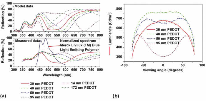 The emission spectrum of the blue LEP investigated is also shown in Fig. 3 and, in the ideal case, the PEDOT thickness should be chosen such that the dip in reflectivity is in the same wavelength range as this emission, since the microcavity acts as a filter. Emission wavelengths which fall outside of this dip are to a large part kept inside the microcavity. It can be seen that for PEDOT thicknesses from 30 to 95 nm, the dip in the reflectivity occurs at higher wavelengths than the emission from the polymer, which is centered at 480 nm. We have calculated [Fig. 3 (upper graph)] that in order to have the dip at this wavelength, a PEDOT thickness of 14 nm would be needed. This is too thin to produce reliably for real OLEDs. For a much higher PEDOT thickness of 171.7 nm, a second order resonance occurs. It is, however, disadvantageous to work with this PEDOT thickness due to the large increase in the angle dependence of the emission color that occurs. When changing the viewing angle the location of the dip in reflectivity shifts according to Eq. 2. For the first order, with its minimum at a wavelength of 480 nm, the dip blueshifts by 35 to 445 nm when changing the viewing angle from 0 to 40 deg. For the second order the resonance shifts by 55 nm to a wavelength of 425 nm for the same change in viewing angle. The angle dependence of the luminance for the top-emissive devices with PEDOT thicknesses in the range 30 to 95 nm, is shown in Fig. 3. For 30 nm of PEDOT, the luminance is primarily directed in the forward direction. When increasing the PEDOT thickness to 40 nm, a more Lambertian emission is obtained for viewing angles up to 50 deg. Then for higher PEDOT thicknesses of 50 and 95 nm the luminance peaks at higher angles of 40 to 70 deg. These angle dependent profiles are a result of the shift in wavelength range and in magnitude of the reflectivity dip with the viewing angle and the corresponding change in overlap with the emission spectrum of the light-emitting material. For example, when the PEDOT thickness is 95 nm the overlap of the dip in reflectivity with the emission spectrum is poor at 0 deg viewing angle, resulting in a low luminance, but the dip shifts closer to the emission at higher angles, resulting in a peak in the luminance at viewing angles of 60 to 70 deg. We have also modeled the angle dependence of luminance from the top-emissive OLEDs both with and without the thin-film-encapsulation stack using SETFOS software from Fluxim in order to determine the effect of adding this thin-film-encapsulation. It was found that the general shape of the angle dependent emission profiles for different PEDOT thicknesses [as seen in the measurements on devices in Fig. 3], including a drop-off in luminance at angles above 60 to 70 deg, could already be modeled by just considering the microcavity effects within the top-emissive OLED structures before the addition of thin-film-encapsulation. It is seen that the effect of adding the thin-film-encapsulation stack is to further steepen the drop-off in luminance at angles above 40 to 50 deg compared to the bare OLEDs for all the different PEDOT thicknesses. The luminous efficacies (integrated over all forward angles in order to take into account the angle dependence of the emission), as well as the power efficacies, are shown in Table 2 for the different PEDOT layer thicknesses. As in this paper we are focusing more on the effects of changing the device structure on the optical performance of the devices and less on the electrical behavior, we will mostly compare the devices in terms of their luminous efficacies. It can be seen that the maximum efficacy of 9.8 lm/A occurs for a layer thickness of 40 nm which was the same device for which the Lambertian emission profile was seen [Fig. 3]. (A maximum in the power efficacy is also found when PEDOT thicknesses of around 40 to 50 nm are used.) However, this device does still show an angle dependence of the emission color with a change in u′v′ color coordinates (CIE1976 diagram) of Δu′v′ = 0.065 going from a viewing angle of 0 deg to 80 deg (Δu′v′ = 0.01 is already visible to the human eye). All of the devices in this series show a color variation with a similar size to this with the emission color going from green to blue as the viewing angle increases. Table 2Luminous efficacy integrated over all forward angles, and power efficacies, for top-emissive OLEDs on stainless steel foil (Foil 2) with different PEDOT thicknesses run at a current density of 238 A/m2.
3.2.Influence of Anode Material on the CavityIn Sec. 3.1 the importance of having an optimal PEDOT layer thickness in top-emissive OLEDs on metal foils was discussed. When determining the optimal layer thicknesses it is important to also consider the optical properties of the metal foil substrate that is used. Even foils made from the same material can have significantly different optical properties and will therefore require different PEDOT layer thicknesses in an optimized device. It can be seen from Eqs. 1, 2 that the phase for both wide angle as well as multiple beam interference is not only influenced by the optical distance between the mirrors, but also by the phase shift at the mirrors. Table 3 gives an overview of the optical properties of some of the metal substrates that we have investigated including their complex refractive indices n′ and n″, the total measured reflection for light with a wavelength of 480 nm, the phase shift at the reflector when going from PEDOT to the substrate material (both taken as semi-infinite media), and the calculated PEDOT thickness that would be required in order to obtain the maximum dip in reflectivity at a wavelength of 480 nm for the first and second order. Table 3Overview of the optical properties of some metal substrates that have been investigated and the subsequent calculated values for PEDOT layer thicknesses required in order to have an overlap of the dip in the reflectivity spectrum with the emission spectrum of the blue light-emitting polymer used.
From these measurements and calculations it is clear that the required PEDOT thickness depends on the properties of the bottom metal substrate, but still for a range of different substrates the optimal first order PEDOT layer thickness for blue-emitting devices is too low for the typical coating techniques used in the fabrication of OLEDs. 3.3.Foil RoughnessThe OLEDs described in this work were made directly on (rough) metal foil substrates. It was important for us to understand the effect that the foil roughness has on the performance of the OLEDs produced, in order to identify the advantages and disadvantages of this approach compared to planarizing the metal foil. In Fig. 4 the profiles of luminance (normalized in upper graph and absolute values in the lower graph) as a function of viewing angle, for a number of different foils with different surface topologies (as described in Table 1) are shown. From the normalized plots, the value of the luminance at 0 deg viewing angle can be taken as an indication of the extent of angle dependence of the emission. For these devices where the luminance peaks at angles higher than 0 deg (PEDOT thickness was 90 nm), the lower the angle dependence is, the closer to 1 the normalized luminance at 0 deg will be. Fig. 4(a) Luminance as a function of viewing angle for top-emissive OLEDs on different stainless steel metal substrate foils normalized (upper graph) and absolute values (lower graph where the ratio of the diffuse to the total reflectivity for Foil 5 and Foil 6 are given on the plot). (b) Normalized luminance (filled squares) and integrated efficacy (open triangles) as a function of the ratio of the diffuse to the total reflection for the different metal substrate foils. 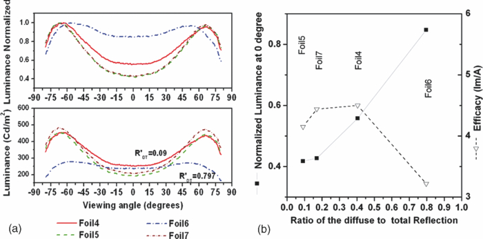 To characterize the scattering power of surfaces, reflection measurements can be performed where a distinction is made between total and diffuse reflection. By integrating the diffuse reflection and the total reflection over a wavelength range which is relevant for the emission spectrum of the polymer, and dividing the two, a ratio, R′DT, is obtained which is a measure for the scatter power of the foil. In Fig. 4 the values of the normalized luminance at 0 deg as well as the integrated efficacy of the devices are plotted as a function of the ratio of diffuse to total reflection. Although only four foils have been measured the effect of increasing the topology of the foil (increased diffuse reflection) is clear. In Fig. 4 (lower graph) it can be seen that the foil with the highest amount of diffuse reflection has lost luminance in the peaks of high angle emission that are seen from devices on other foils with the same PEDOT thickness but lower diffuse reflection. So although the angle dependence of the luminance has reduced, this is at the expense of efficacy. This effect is shown more quantitatively in Fig. 4 where an increase in the proportion of the luminance seen at 0 deg viewing angle can be seen as the amount of diffuse reflection increases. The integrated efficacy then decreases as the ratio of diffuse to total reflection is increasing. For the device made on Foil 6, which has the highest R′DT, the emission appears blue at all viewing angles as a result of the increased scattering of light within the structure that acts to mix angle-dependent emission color characteristics. The color variation in this case, for viewing angles of 0 to 80 deg, is Δu′v′ = 0.034. This is lower than that for the devices made on the smoother Foil 2 (described in Sec. 3.1), but it is still detectable by eye. The current-voltage characteristics of the devices (Fig. 5) were fairly similar for all of the different foils, with the exception of Foil 6 which has the largest topology and had more leakage current. Therefore devices on this foil show lower efficacies in the lower voltage range. At higher voltages the efficacies of all of the devices became comparable for a viewing angle of 0 deg. There was no change in the shape of the angle dependent luminance profile with the voltage applied to a particular device. Fig. 5Current density (solid lines) and luminance (dashed lines) as a function of applied voltage for OLEDs made on stainless steel foils of different roughness's (PEDOT thickness 90 nm). The luminance in this plot is the value measured perpendicular to the devices, but due to the strong angle dependence of the emission [Fig. 4] the luminance integrated over all viewing angles must be used in order to calculate the efficacy [Fig. 4] which is then in lm/A. 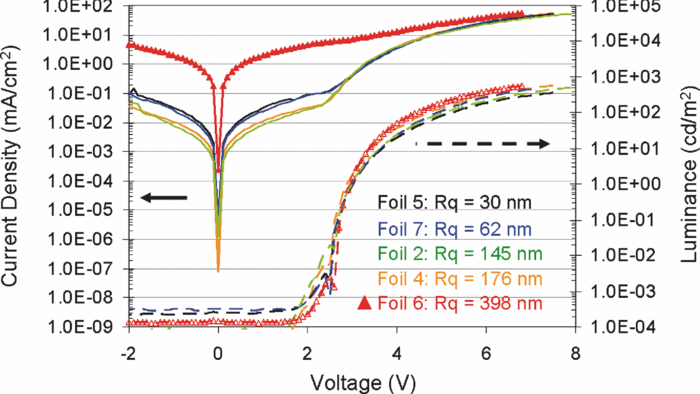 4.Discussion4.1.Optimization of Microcavity for Devices on FoilWe have been able to achieve an improvement in the efficacy and angle dependence of emission for top-emissive OLEDs on stainless steel foil substrates, by variation of the PEDOT layer thickness. As the PEDOT layer thickness was increased from 30 to 95 nm the efficacy went through a maximum and the angle dependence of the luminance changed from being in the forward direction to Lambertian to peaking at a viewing angle of 65 deg. The emission spectrum of the OLED is redshifted with increasing cavity length and blueshifted with increasing viewing angle (consistent with resonance conditions for an optical cavity). These are all similar trends to those observed when optimizing top-emissive OLEDs fabricated on smooth glass substrates.22 Typically it is seen that it is very difficult to simultaneously achieve a maximum in the efficacy and a minimum in the variation of color and luminance with viewing angle in top-emissive devices, since the optimal layer thicknesses for the best efficacy and the best color performance are usually different.22 In the system that we investigated on stainless steel foil we do actually achieve a coincidence of the maximum efficacy of 9.8 lm/A and a Lambertian emission profile for the same PEDOT layer thickness of 40 nm. For comparison, the efficacy of bottom-emissive devices on glass made with the same blue-emitting LEP is 16.3 lm/A (2.4lm/W) and there is a far lower variation in device performance when the PEDOT layer thickness is changed. When using optical modeling to determine the PEDOT layer thickness that would give the best overlap of the dip in the reflectivity spectrum with the emission spectrum a first order value of 14 nm and a second order value of 171.7 nm were found. This suggests that with our experimentally determined value of 40 nm we have not really found the optimum device structure, and that in theory it may be possible to achieve an even higher efficacy. The reason that we appear to have achieved a maximum experimentally is the blueshift in emission color that occurs when reducing the PEDOT layer thickness. This color change will have an effect in reducing the luminous efficacy for the devices with thinner PEDOT layers and suppressing the luminance for higher angle emission. Unfortunately PEDOT thicknesses lower than 20 to 30 nm could not be produced reliably or uniformly experimentally, so our results for 30 to 40 nm PEDOT are likely to be the best first order results. For the second order PEDOT thickness of 171.7 nm the angle dependence of the emission is expected to be relatively high. In this initial test of optimization of the microcavity for top-emissive OLEDs on metal foils we have only varied the PEDOT layer thickness, but other layer thicknesses such as the LEP and the cathode stack could also be varied for further optimization of the device performance. In addition, the reflectivities of the stainless steel foils are relatively low (48 % to 59 %), compared to materials such as silver and aluminium (see Table 3), due to absorption of light by this substrate. From Eq. 1 it is clearly advantageous for the performance of the microcavity to have the reflectivity (RA) of the metal foil anode as high as possible. The modeled reflectivity spectra for a smooth Ag/Cr anode layer on a glass substrate (optical data given in Table 3), are compared to those modeled for a stainless steel foil in Fig. 6. The PEDOT thicknesses have been chosen to give either the first or second order dip at a wavelength of 480 nm (the center of the emission spectrum of the LEP investigated). These PEDOT thicknesses are given in Table 3 and are seen to be relatively similar for the two different anode materials. The main difference is that the overall reflectivity values for the Ag substrate are higher than those for stainless steel, so there is less absorption of the light as it undergoes multiple reflections within the microcavity structure. Fig. 6Comparison of modeled reflectivity spectra for top–emissive OLEDs made on Ag and on stainless steel (Foil 2) foil. The PEDOT thickness is optimized such that either a first order or a second order dip in the reflectivity occurs at 480 nm and the thicknesses required for this are given in Table 3. 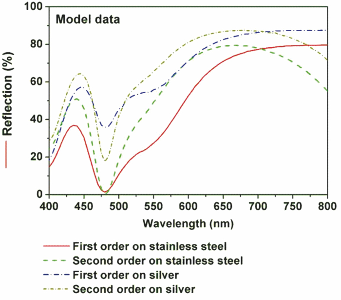 4.2.Influence of Substrate Roughness on Performance of OLEDsThe top-emissive OLEDs described in this paper are based on metal foils that have significant surface topology. As an example, the topology of one of the stainless steel foils investigated (Foil 2) is shown in the white light interferometry image in Fig. 7. A pattern of rolling lines can clearly be seen in this foil (as was also the case for most of the other foils that were investigated). It was shown for the OLEDs presented in Sec. 3.3 that as this topology is increased the high angle emission is suppressed which reduces the angle dependence of the emission, but also decreases the efficacy of the devices. This effect can be understood by considering the combination of two effects. First that the amplitudes and frequencies of the foil topology enable the scattering of light [Fig. 7],27 and second that the coating of the thin PEDOT and LEP layers over the rough metal foils is likely to result in local variations in layer thicknesses. Fig. 7(a) Image of the topology of Foil 2 taken using white light interferometry. (b) Schematic diagram showing the diffraction orders bn at angles θn, when light is incident at angle θi to the normal of a rough substrate. (c) Microscope image of the electroluminescence from a top-emissive OLED made on Foil 2 [image not taken at the same position on the foil as (a)]. 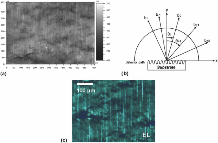 According to the Fraunhofer diffraction theory27 the diffraction from a sinusoidal structure can be described by [TeX:] \documentclass[12pt]{minimal}\begin{document}\begin{equation}
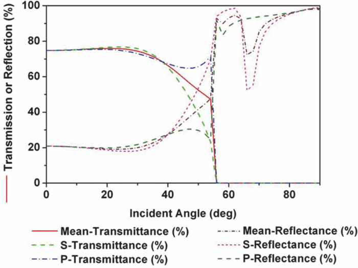
\sin \theta _n = \sin \theta _i = nf_g \lambda
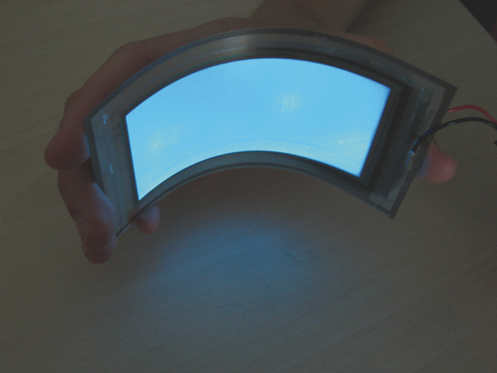
\end{equation}\end{document} where θn is the angle at which the n'th order is reflected, θi is the angle of incidence of the incoming light, fg is the frequency of the roughness, and λ is the wavelength of the light.Equation 4 is only applicable to sinusoidal structures. The roughness of metal foils is a superposition of more than one spatial frequency. According to Stover,27 the diffraction principle is still applicable, but it becomes more complex. A method to describe the diffuse reflection is to use the surface power spectral density of the roughness which is applicable for sinusoidal structures. The bidirectional reflection distribution functions (BRDF) such as described in Ref. 28 are used to describe scattered light patterns. In the case of the stainless steel foils that we have investigated, Fourier transforms of the topology data did not reveal any dominant frequencies for the occurrence of rolling line features, just a steady decrease in the power spectral density with increasing frequency. Even from the simple approach of Eq. 4, which relates the frequency of the roughness to the scatter angle, it can be seen that rough surfaces will scatter an incident ray of light into many angles. For any of these angles that are higher than the critical angle for escaping the device structure, the light will miss a chance of escaping from the OLED and have to rely on further reflections and scattering events in order to escape. However there is a high probability that it will be absorbed instead. For the relatively smooth foil investigated in Sec. 3.1 a variation in the angle dependence of the luminance profile could be created by changing the PEDOT layer thickness. However, for the rougher foils the emission will always tend to be closer to Lambertian, which is a way of controlling the angle dependence of luminance, but at the expense of efficacy compared to the smoother foils. The effect of changing the metal foil roughness on the OLED performance is also likely to result, in part, from local variations in the PEDOT and LEP layer thicknesses. Backscatter electron images taken with SEM on PEDOT-coated stainless steel foils reveal that the amount of light atomic materials is higher in some places than others, and these positions correlate with the structure of the foil. This strongly suggests a variation in the local thickness of the PEDOT on top of the metal foil. Further evidence for this comes from microscope images of the electroluminescence of OLEDs on stainless steel foils [Fig. 7] where stripes of brighter and darker emission can be seen. These seem to resemble the topology of the metal foil substrate, suggesting that there are regions where the PEDOT layer thickness is more optimal for the device efficacy or where the light-emitting polymer layer is thinner (resulting in a locally higher electric field for a given applied voltage and therefore brighter emission). From Fig. 5 it was also seen that devices made on the roughest stainless steel foil did have a higher leakage current than the others, suggesting some areas with thinner LEP than for devices on smoother foil substrates. The reflectivity spectra of complete OLED devices also indicate variations in layer thicknesses within one device and changes in the propagation angle of light due to scattering, as a broadening of the reflectivity dip is seen with increasing foil topology (not shown here). This is likely to be caused by sampling many different PEDOT and LEP layer thicknesses and propagation angles within the device, each of which have their dip in reflectivity at different wavelengths. These broader (and shallower) dips in the reflectivity spectra for the roughest foils correspond to a reduction in the luminance and its angle dependence. The transparent cathode stack that is applied to the device will also have an effect on the efficacy and the angle dependence of the emission. Figure 8 shows the modeled transmission and reflection versus angle when taking LEP as the incident medium, followed by a cathode and a capping layer after which the light enters a thin-film-encapsulation stack. Even before the angle of total internal reflection is reached, it can be seen that the reflection increases and hence transmission decreases, which may act to reduce the amount of light that can get out of the structure if there is a lot of absorption within the microcavity. 5.ConclusionWe have investigated the optimization of the efficacy and angle dependence of emission of blue-emitting top-emissive OLEDs on (rough) metal foils. We find that by adjusting the PEDOT layer thickness in the range 30 to 95 nm a maximum efficacy of 9.8 lm/A is reached for a PEDOT thickness of 40 nm. This is 60% of the value of 16.3 lm/A found for bottom-emissive devices made on glass substrates for the same light-emitting polymer. The luminance for this top-emissive device has a Lambertian profile, but the color variation over the range of viewing angles from 0 to 80 deg is detectible by eye (Δu′v′ = 0.065). The microcavity effects that we observe appear to be similar to those already published for top-emissive OLEDs on smooth substrates.22 However we believe that further optimization is possible for this device structure as model calculations showed that some PEDOT layer thicknesses outside of the range 30 to 95 nm result in a better overlap of the emission spectrum with the dip in the reflectivity spectrum of the devices. Variation of other device layer thicknesses and an increase in the reflectivity of the anode material should also improve the performance. So even when making devices on relatively rough metal foils it is still possible to achieve performances that are coming quite close to those of standard bottom-emissive devices. The metal foil topology does have an important effect on the device performance though as the efficacy is seen to decrease with increasing topology and the emission profile tends toward being Lambertian. A photograph of a working 5 cm × 10 cm, thin-film-encapsulated, top-emissive device on stainless steel foil is shown in Fig. 9. Similar devices with active areas of up to 12 cm × 12 cm have also been made with close to 100% production yield. For lighting applications a color conversion layer could be added in order to achieve white emission. In this case the device architecture and emission spectrum of the light-emitting material (peak wavelength and width), would always need to be optimized with a view to achieving a good overlap of the dip of the reflectivity spectrum of the device with the emission spectrum occurring in the blue spectral range. Considering the results presented in this paper, we feel that top-emissive OLEDs on metal foil substrates are a realistic prospect for lighting and signage applications. AcknowledgmentsThe Holst Centre is an open innovation research center founded by TNO and IMEC that is developing roll-to-roll production techniques for foil-based organic electronics and wireless autonomous transducer solutions, in cooperation with industry and universities.29 This particular research has been funded by the Dutch Ministry of Economic Affairs, Philips Research, Agfa, and Solvay. We gratefully acknowledge Merck for providing the light-emitting polymer material, Henri Jagt (Philips Research) for use of a spectrophotometer, Frank van Abeelen for his valuable input about microcavity optics, and Hugo Cornelissen (Philips Research) for his assistance in measuring the devices. ReferencesH. Yokoyama,
“Physics and device applications of optical microcavities,”
Science, 256 66
–70
(1992). http://dx.doi.org/10.1126/science.256.5053.66 Google Scholar
V. Cannella, M. Izu, S. Jones, S. Wagner, and I.-C. Cheng,
“Flexible stainless steel substrates,”
SID Magazine, 21 24
–27
(2005). http://dx.doi.org/http://www.sidmembers.org/idonline/article.cfm?year=2005&issue=06&file=art5 Google Scholar
D. U. Jin, J. K. Jeong, H. S. Shin, M. K. Kim, T. K. Ahn, S. Y. Kwon, J. H. Kwack, T. W. Kim, Y. G. Mo, and H. K. Chung,
“5.6-inch flexible full color top emission AMOLED display on stainless steel foil,”
SID Int. Sympo. Digest Tech. Papers, 37 1855
–1857
(2006). http://dx.doi.org/10.1889/1.2433405 Google Scholar
A. Chwang, R. Hewitt, K. Urbanik, J. Silvernail, K. Rajan, M. Hack, J. Brown, J. P. Lu, C. Shih, J. Ho, R. Street, T. Ramos, L. Moro, N. Rutherford, K. Tognoni, B. Anderson, and D. Huffman,
“Full color 100 dpi AMOLED displays on flexible stainless steel substrates,”
SID Int. Sym. Digest Tech. Papers, 37 1858
–1861
(2006). http://dx.doi.org/10.1889/1.2433406 Google Scholar
R.-Q. Ma, K. Rajan, M. Hack, J. J. Brown, J. H. Cheon, S. H. Kim, M. H. Kang, W. G. Lee, and J. Jang,
“Highly flexible low power consumption AMOLED displays on ultra-thin stainless steel substrates,”
SID Int. Symp. Digest Tech. Papers, 39 425
–428
(2008). http://dx.doi.org/10.1889/1.3069689 Google Scholar
A. W. Lu and A. D. Rakić,
“Design of microcavity organic light emitting diodes with optimized electrical and optical performance,”
Appl. Opt., 48 2282
–2289
(2009). http://dx.doi.org/10.1364/AO.48.002282 Google Scholar
D.-S. Leem, S.-Y. Kim, J.-H. Lee, and J.-J. Kim,
“High efficiency p-i-n top-emitting organic light-emitting diodes with a nearly Lambertian emission pattern,”
J. Appl. Phys., 106 063114
(2009). http://dx.doi.org/10.1063/1.3225998 Google Scholar
M. Thomschke, R. Nitsche, M. Furno, and K. Leo,
“Optimized efficiency and angular emission characteristics of white top-emitting organic electroluminescent diodes,”
Appl. Phys. Lett., 94 083303
(2009). http://dx.doi.org/10.1063/1.3088854 Google Scholar
M.-T. Lee and M.-R. Tseng,
“Efficient, long-life and Lambertian source of top-emitting white OLEDs using low-reflectivity molybdenum anode and co-doping technology,”
Curr. Appl. Phys., 8 616
–619
(2008). http://dx.doi.org/10.1016/j.cap.2007.11.002 Google Scholar
Q. Wang, Z. Deng, and D. Ma,
“Realization of high efficiency microcavity top-emitting organic light-emitting diodes with highly saturated colors and negligible angular dependence,”
Appl. Phys. Lett., 94 233306
(2009). http://dx.doi.org/10.1063/1.3153140 Google Scholar
H. W. Joo, W. K. Han, D. H. Chung, J. W. Hong, and T. W. Kim,
“Microcavity effect in compliance with interference of light in Alq3 based top-emission organic light-emitting diodes,”
Mol. Cryst. Liq. Cryst., 520 55/[331]
–59/[335]
(2010). http://dx.doi.org/10.1080/15421401003608469 Google Scholar
X.-W. Zhang, J. Li, L. Zhang, X.-Y. Jiang, K.-u. Haq, W.-Q. Zhu, and Z.-L. Zhang,
“Top-emitting organic light-emitting device with high efficiency and low voltage using a silver–silver microcavity,”
Thin Solid Films, 518 1756
–1759
(2010). http://dx.doi.org/10.1016/j.tsf.2009.11.063 Google Scholar
J.-J. Huang, Y.-K. Su, S.-H. Wang, Y.-H. Liu, and F.-S. Juang,
“Efficiency enhancement of top emission organic light-emitting diodes with Ni/Au periodic anode,”
Jpn. J. Appl. Phys., 47 7359
–7362
(2008). http://dx.doi.org/10.1143/JJAP.47.7359 Google Scholar
M. S. Kim, C. H. Jeong, J. T. Lim, and G. Y. Yeom,
“White top-emitting organic light-emitting diodes using one-emissive layer of the DCJTB doped DPVBi layer,”
Thin Solid Films, 516 3590
–3594
(2008). http://dx.doi.org/10.1016/j.tsf.2007.08.078 Google Scholar
C.-J. Yang, S.-H. Liu, H.-H. Hsieh, C.-C. Liu, T.-Y. Cho, and C.-C. Wu,
“Microcavity top-emitting organic light-emitting devices integrated with microlens arrays: Simultaneous enhancement of quantum efficiency, cd/A efficiency, color performances, and image resolution,”
Appl. Phys. Lett., 91 253508
(2007). http://dx.doi.org/10.1063/1.2827182 Google Scholar
Q. Wang, Z. Deng, J. Chen, and D. Ma,
“Realization of blue, green, and white inverted microcavity top-emitting organic light-emitting devices based on the same emitting layer,”
Opt. Lett., 35 462
–464
(2010). http://dx.doi.org/10.1364/OL.35.000462 Google Scholar
X. Zhu, J. Sun, X. Yu, M. Wong, and H.-S. Kwok,
“High-performance top-emitting white organic light-emitting devices,”
Jpn. J. Appl. Phys., 46 4054
–4058
(2007). http://dx.doi.org/10.1143/JJAP.46.4054 Google Scholar
H. Riel, S. Karg, T. Beierlein, B. Ruhstaller, and W. Rieß,
“Phosphorescent top-emitting organic light-emitting devices with improved light outcoupling,”
Appl. Phys. Lett., 82 466
–468
(2003). http://dx.doi.org/10.1063/1.1537052 Google Scholar
K. A. Neyts,
“Simulation of light emission from thin-film microcavities,”
J. Opt. Soc. Am. A, 15 962
–971
(1998). http://dx.doi.org/10.1364/JOSAA.15.000962 Google Scholar
X.-W. Chen, W. C. H. Choy, D. He, and P. C. Chui,
“Comprehensive analysis and optimal design of top-emitting organic light-emitting devices,”
J. Appl. Phys., 101 113107
(2007). http://dx.doi.org/10.1063/1.2739220 Google Scholar
C. C. Wu, C. L. Lin, P. Y. Hsieh, and H. H. Chiang,
“Methodology for optimizing viewing characteristics of top-emitting organic light-emitting devices,”
Appl. Phys. Lett., 84 3966
–3968
(2004). http://dx.doi.org/10.1063/1.1745107 Google Scholar
S. A. Ahkmanov and S. Yu. Nikitin, Physical Optics, Oxford University Press, New York
(1997). Google Scholar
H. Peng, J. Sun, X. Zhu, X. Yu, M. Wong, and H. S. Kwok,
“High-efficiency microcavity top-emitting organic light-emitting diodes using silver anode,”
Appl. Phys. Lett., 88 073517
(2006). http://dx.doi.org/10.1063/1.2172734 Google Scholar
C. Tanase, P. van de Weijer, H. Lifka, and G. Rietjens,
“Thin film encapsulated transparent organic light emitting diodes,”
Mater. Res. Soc. Symp. Proc., 1091-AA13-08 Warrendale, PA
(2008). Google Scholar
F. van Assche, H. Rooms, E. Young, J. Michels, T. van Mol, G. Rietjens, P. van de Weijer, and P. Bouten,
“Thin-film barrier on film for organic LED lamps,”
(2008). Google Scholar
J. C. Stover,
“Optical Scattering Measurement and Analysis,”
(1995) Google Scholar
W. A. P. Smith and E. R. Hancock,
“A unified model of specular and diffuse reflectance for rough, glossy surfaces,”
643
–650
(2009). http://dx.doi.org/10.1109/CVPR.2009.5206498 Google Scholar
BiographyHarmen Rooms started as a research engineer at Holst Centre in 2006 in the Printed Organic Lighting and Signage program. His work has been mainly on characterization, analysis, and optical modeling of OLEDs for lighting and signage devices. In 2003 he received his bachelor degree in applied physics from Fontys Hogescholen in Eindhoven which was concluded with a project researching the possibilities for quality assessment of DVD-R substrates using diffraction measurements. He started working at Philips in 2004 in the area of characterization of materials for OLED displays. In 2005 he started working at OTB, an SME specialized in developing production machines for various markets such as solar cells and at that time OLED screens. There he was responsible for analysis using a multitude of analysis techniques. Dorothee Hermes is a process engineer in the Printed Organic Lighting and Signage program at Holst Centre and is responsible for the design and fabrication of top-emissive OLED devices. She received her Dipl-Ing degree in biomedical engineering at the University of Applied Sciences of Aachen in 2002. After this she worked as a cleanroom process engineer in the field of biosensors and microfluidics at the MESA+ Research Institute of the University of Twente and as a R&D engineer at Micronit Microfluidics BV in Enschede. She joined the Holst Centre in 2006. Stephan Harkema is a senior scientist in the Printed Organic Lighting and Signage program at Holst Centre. He received his PhD in polymer chemistry from the University of Groningen in 2005 on the topic of harnessing capillary instabilities in thin polymer films. After this he worked as a scientist at TNO Science & Industry in Eindhoven (NL) from 2005 to 2007 on the topic of blue light-emitting fluorene copolymers for OLED applications before joining the Holst Centre in 2007. Ton van Mol is the program manager of the Printed Organic Lighting and Signage program and the Electrodes and Barriers program at Holst Centre. He received his PhD in 2001 at the Eindhoven University of Technology on the study of atmospheric pressure chemical vapor deposition (APCVD) of tin oxide coatings. In 2002 he was a visiting scientist at Sandia National Laboratories, Livermore California, where he continued his research on the APCVD of SnO2:F on glass for low-E coatings. After this, he was a project manager at TNO for the Helianthos program, a joint collaboration with Akzo-Nobel (which sold this activity in 2005 to Nuon) on the development of R2R solar cells before joining Holst Centre in 2006. Paul W. M. Blom received his Ir Degree (physics) in 1988 and his PhD degree in 1992, from the Eindhoven University of Technology, Eindhoven, The Netherlands. His thesis work was on picosecond charge carrier dynamics in GaAs quantum wells. He then worked at Philips Research Laboratories on the electrical characterization of various oxidic thin-film devices and the electro-optical properties of polymer light-emitting diodes, and he also worked in the field of rewritable optical storage based on phase-change and magneto-optical recording using blue laser diodes. In May 2000 he was appointed as a professor at the University of Groningen, leading a group in the field of electrical and optical properties of organic semiconducting devices. The main research focus of the group is on the device physics of polymeric light-emitting diodes, transistors, and solar cells. In 2008 he was appointed as the scientific director of the Holst Centre in Eindhoven where the focus of his work is on the realization of foil-based electronic systems. Joanne Wilson is a senior scientist in the Printed Organic Lighting and Signage program at the Holst Centre. She received her PhD in organic electronics from the University of Cambridge (UK) in 2001 on the topic of triplet states in conjugated polymers. After this she worked as a research fellow and research lecturer at Imperial College London in areas including the photophysics of conjugated polymers, phosphorescent OLEDs, and organic photovoltaics before joining the Holst Centre in 2006. |
|||||||||||||||||||||||||||||||||||||||||||||||||||||||||||||||||||||||||||||||||||||||||||||||||||||||||||||||||||||||||||||||||||||||||||||||||||||||