|
|
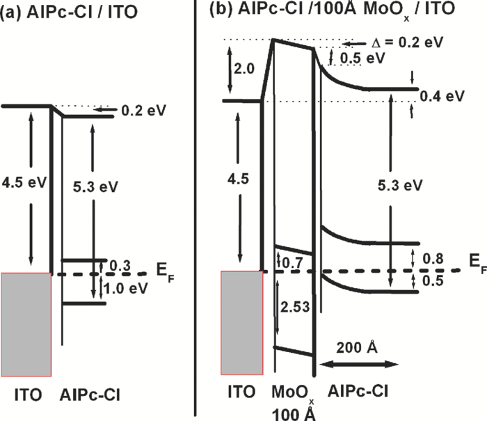
1.IntroductionOrganic semiconductors have been demonstrated for their potential in applications including organic photovoltaic (OPV),1−5 organic light-emitting diode (OLED),6−8 organic thin-film transistor,9, 10 as well as in efficient spin injection in organic materials.11, 12 OPV has attracted an enormous amount of attention due to growing energy requirements of the world and declining fossil resources.13 OPV cells offer considerable advantages over crystalline inorganic photovoltaic devices in terms of lower production cost and versatility of applications, such as lightweight, large-area, and flexible solar panels along with being more ecofriendly. A great deal of effort has been made in order to improve the charge transport and collection at the electrodes. Introduction of a high work-function (WF) transition metal oxide insertion layer between conducting indium tin oxide (ITO) and organic semiconductors was an attempt made by Tokito et al.14 More recently, it was reported that improved hole injection and stable device performance can be achieved by the insertion of a molybdenum oxide (MoOx) interlayer in OLED.15, 16 In OPV research, metal oxide as an interlayer between the ITO anode and the hole-collection layer was successfully demonstrated by Shrotriya et al.17 Irwin et al.18 has also demonstrated the efficiency enhancement by a thin nickel oxide insertion layer. Our recent results show 20% improvement in the fill factor and 35% reduction in the series resistance for MoOx interlayer between ITO anode and chloro-aluminum pthalocyanine (AlPc-Cl).19 The observations raised questions of how an insulating layer may reduce the resistivity, what the optimum thickness of such insertion layer is, and what the mechanism of this improvement is. Recently, Kroger et al.20 reported a possible mechanism for hole-injection improvement, originating from electron extraction from the highest occupied molecular orbital (HOMO) of organic semiconductor to the ITO anode through conduction band of MoOx. In our very recent report,21 we have established the efficiency enhancement due to a reduced hole-injection barrier and a drift field due to the hole accumulation at the ITO/hole-injection layer. The growing interest in transition metal oxides insertion layer, MoOx in particular, creates an urgent need to conduct a detail study of its electronic properties and the changes it can undergo in normal handling and fabrication processes. We discussed the importance of the high MoOx WF as a crucial factor in the performance enhancement of OPV devices.21 However, the surface WF of MoOx has been reported as 5.3, 5.68, and 6.86 eV by Shrotriya,17 Matasushima et al.,22 and Kroger,20, 23 respectively, in spite of the fact that all the groups used the same technique, ultraviolet photoemission spectroscopy (UPS), to determine the WF. Additionally, in our most recent studies,24, 25 we have reported deteriorating effects of air exposure on the device performance. It is imperative to resolve the discrepancy in order to understand how to control the device fabrication and to obtain consistent device performance. In this paper, we report our systematic investigation of MoOx films with various parameters to optimize device efficiency enhancement using UPS, inverse photoemission spectroscopy (IPES) and x-ray photoemission spectroscopy (XPS). We will present the electronic energy level evolution of AlPc-Cl/ITO interface with and without MoOx insertion layer and discuss the beneficial nature of the insertion layer. We will also discuss the mechanism responsible for this counterintuitive phenomenon of device performance enhancement and optimum thickness of the insertion layer. We found a shift to high surface WF values on deposition of MoOx on ITO. The high surface WF lifted the HOMO level of the organic and reduced the barrier at the interface. As the organic thickness increases, its energy levels relaxed toward its bulk value, creating a band-bending-like region in the organic side. We will further discuss the electronic energy level evolution of controlled air and oxygen exposed MoOx films. We monitored the changes in the valence electronic structure, WF, and ionization potential of the surface as a function of air and oxygen exposure. We found that the vacuum-deposited MoOx films started with high initial WF values, but with air and oxygen exposure the surface WF gradually reduced to much lower values. The reduction is attributed to chemisorption of oxygen and moisture on the MoOx surface. We also observed growth of an interface electronic state in the energy gap with increasing exposure both in the air and oxygen. The reduction was initially dominated by oxygen adsorption at exposure <1013 L, and finally saturated by moisture at 1014 L. 2.ExperimentsUPS, IPES, and XPS studies were performed using a VG ESCA Lab, an ultrahigh vacuum (UHV) system equipped with a He discharge lamp and a Mg Kα x-ray source (1253.6 eV). The UHV system consists of three interconnecting chambers, a spectrometer chamber, an in-situ oxygen plasma (OP) treatment chamber, and an evaporation chamber with a precision air leak valve. The base pressure of the spectrometer chamber is typically 8 × 10⁻¹¹ Torr. The base pressure of the evaporation chamber is typically 1 × 10⁻⁶ Torr. The UPS spectra were recorded by using unfiltered He I (21.2 eV) excitation, as the excitation source with the sample biased at −5.00 V to observe the low-energy secondary cutoff. The UV light spot size on the sample is ∼1 mm diam. The typical instrumental resolution for UPS measurements ranges from 0.03 to 0.1 eV with the photon energy dispersion of <20 meV. The XPS resolution is ∼1.4 eV. The IPES spectra were recorded using a custom-made spectrometer, composed of a commercial Kimball Physics ELG-2 electron gun and a bandpass photon detector. The photon detector worked in the isochromat mode centered at a fixed energy of 9.8 eV. The sample was kept at ∼2 cm away from the e-gun, introducing an electron beam spot of ∼1 mm diam on the sample surface. The combined resolution (electron + photon) of the IPES spectrometer was determined to be ∼0.6 eV from the width of the Fermi edge measured on a clean polycrystalline Au film. The air and oxygen exposure experiment were carried on two ITO substrates cut from a borosilicate glass sheet from Corning, Inc. (Corning, NY). The glass sheet was coated with 250-nm-thick conducting ITO, with resistivity 15 Ω per square. The substrates were treated in situ in oxygen ambience26 of 600 milli-Torr at bias voltage of –500 V for 30 s. 50 A thick thermally evaporated MoOx films were deposited on both OP-treated ITO substrates. The thicknesses of the MoOx films were monitored with quartz crystal microbalance. The first MoOx film was exposed to air in controlled steps of 102, 104, 106, 108, 1010, 1011, 1012, 5 × 10¹², 1013, 5 × 10¹³, 1014, and 2 × 10¹⁴ L. One Langmuir (L) exposure is equal to the 10−6 Torr-s exposure, the amount for one monolayer adsorption when the gas sticking coefficient is unity. The second MoOx film was exposed to oxygen in controlled steps of 1, 102, 104, 106, 108, 1010, 1012, 5 × 10¹², 1013, 1014, and 5 × 10¹⁴ L. The exposures up to 104 L were performed inside the spectrometer chamber, and the remaining exposures were performed in the evaporation chamber. The oxygen exposures were performed by using ultrapure carrier-grade oxygen (UN 1072) from the Airgas Inc. (Salem, NH). The dry air has ∼20.95% oxygen by volume, and thus, the oxygen exposure of 2 × 10¹⁴ L is similar to the dry air exposure of ∼1015 L in terms of the effect of oxygen on the surface. The relative humidity in the laboratory was ∼33% during the air exposure. The surface topography data were obtained with Nanoscope III (from Digital/Vecco) atomic force microscope (AFM) in tapping mode with silicon tips. All the measurements were performed at room temperature. 3.Results and Discussions3.1.Effect of MoOx Insertion Layer between Indium Tin Oxice and AlPc-ClIt is well known that the control of the electronic structure and the complex interactions at the electrode/organic interface can significantly affect the device efficiency and lifetime.14−18 For example, a great deal of work has been performed to modify a conducting ITO anode26, 27 surface, which includes oxygen plasma, thermal annealing, and various kinds of insertion layers as well. A description of an organic semiconductor/electrode interface and energy level alignment can be found in recent review articles.28, 29 In a recent work from one of us, the effect of molybdenum oxide (MoOx) insertion layer on both small molecule organic photovoltaic cells as well as polymer photovoltaic cells was studied. The results suggest that with the presence of MoOx insertion layer, the power conversion efficiencies were enhanced by a maximum of 38% due to a significant enhancement in the fill factor.19 In the early studies of OLED devices, the improvement from MoOx insertion layer is usually attributed largely to the reduction of the hole injection barrier at the organic hole transport layer/ITO anode interface. However, this may not explain the role of MoOx insertion layer in OPV, because one is not injecting any charges in this case, rather extracting holes from the organic hole transport layer to the ITO anode. Therefore, further investigations are necessary to understand the origin of such improvement. In this section, we will discuss the electronic energy-level evolution at the chloro-aluminum pthalocyanine (AlPc-Cl)/ITO interface with and without a 10-nm MoOx insertion layer and based on energy-level alignment, we will explain mechanism encouraging OPV device efficiency enhancement. We found that deposition of MoOx abruptly increases the surface WF due to which all the energy levels of subsequently deposited AlPc-Cl shift toward the lower binding energy (BE) at the interface, and as a result, there is a strong hole accumulation at the AlPc-Cl/MoOx interface. With increasing AlPc-Cl thickness, the energy levels shift back gradually toward the lower BE. This relaxation creates a band-bending-like region in the hole transport layer (AlPc-Cl) and introduces the hole drift component to the already existing hole diffusion current. The electronic energy-level evolution of the cutoff and the HOMO region for AlPc-Cl deposited on ITO are shown in Figs. 1 and 1, respectively. The ITO substrate used in this experiment are ex situ OP treated, and WF values may be different from the in situ treated ones, which is consistent with earlier reports.26 The ITO WF was measured to be 4.56 eV. In Fig. 1, we can see fast saturation of WF as overlaying AlPc-Cl thickness increases. We also note the overall WF shift is ∼0.2 eV and at the 16-Å AlPc-Cl deposition, the WF shift nearly saturated. At the 64 Å of AlPc-Cl deposition, the work function was measured to be 4.33 eV. From the data presented in Fig. 1, it is clear that the frontier-occupied levels were fully developed after 32 Å of AlPc-Cl deposition. Four peaks belonging to the AlPc-Cl are clearly visible in the scanned BE range. Binding energies of these peak are measured to be 1.45, 3.63, 5.23, and 6.72 eV at 64 Å of AlPc-Cl deposition. Fig. 1UPS data for 64, 32, 16, 8, 4, and 2 Å AlPc-Cl and ITO for (a) the cutoff region and (b) the HOMO region. 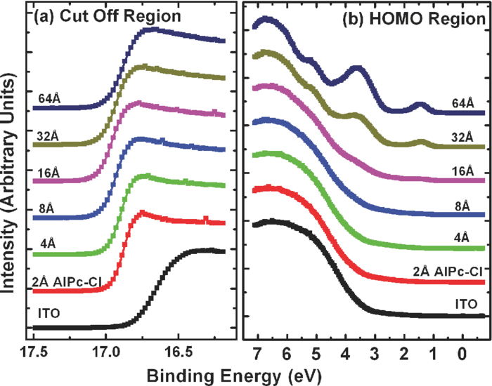 The electronic energy-level evolution shown in Fig. 2 addresses the question of efficiency enhancement reported with an MoOx interlayer.19 All the spectra have been normalized to the same height for visual clarity. In Fig. 2, we observe an abrupt WF shift on the deposition of 100 Å of MoOx. The ex situ OP treated ITO WF was measured to be 4.58 eV, and the deposition of MoOx moved the surface WF value to 6.55 eV, which is ∼2 eV higher than the ITO surface. With the deposition of AlPc-Cl on MoOx/ITO, the WF at first decreased rapidly until 16 Å and then the decrease became slower and more gradual. At 228 Å AlPc-Cl deposition, the surface WF was measured to be 4.92 eV. The HOMO features of AlPc-Cl were observed to develop between 8 and 16 Å. There was a shift ∼0.2 eV toward the higher BE in the MoOx characteristic peak as indicated in Fig. 2, before AlPc-Cl feature were developed. Four strong peaks belonging to the AlPc-Cl occupied levels were observed in the experimental scan range of BE from –1 to 7 eV with respect to the Fermi level of the system. The BE of the occupied level peaks of AlPc-Cl were observed to be about 0.67, 2.81, 4.31, and 5.87 eV for 32 Å of AlPc-Cl. The other interesting effect due to the presence of MoOx interlayer was that all the peaks in the HOMO region of AlPc-Cl kept gradually shifting toward the higher BE. The BE for four occupied level peaks were measured to be 1.11, 32.3, 4.85, and 6.31 eV for 228 Å AlPc-Cl thickness. The shift in the HOMO peak of AlPc-Cl in the investigated thickness range was ∼0.4 eV, as presented in Fig. 2. Fig. 2Electronic energy-level evolution (UPS data) for 228, 128, 64, 32, 16, 8, 4, and 2 Å AlPc-Cl, and ITO with 100 Å MoOx interlayer for (a) the cutoff region and (b) the HOMO region. 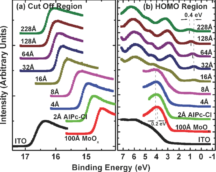 The energy-level alignment diagrams for AlPc-Cl/ITO interface without and with a 100 Å MoOx insertion layer are depicted in Figs. 3 and 3, respectively. A bandgap of 1.3 and 3.2 eV is determined for AlPc-Cl and MoOx, respectively, from our UPS and IEPS data (not shown).21−23 At the AlPc-Cl/ITO interface, an abrupt vacuum level shift of 0.2 eV is observed, which can be attributed as an interface dipole. Increasing thickness of AlPc-Cl results in a flat-band situation, in which the HOMO lies 1.0 eV below the Fermi level of the system. On the other hand, the insertion of the MoOx layer leads to a large increase in the surface WF of ∼2 eV as shown in Fig. 3. Here, the valence-band maximum of the MoOx layer is measured to be ∼2.53 eV below the Fermi level. The large WF of the metal oxide therefore causes an upward shift of all the energy levels of AlPcCl, which results in a strong hole accumulation at the AlPcCl/MoOx interface. This hole accumulation is also reflected in the shift of 0.2 eV in the MoOx peak toward higher binding energy, as a result of the electron transfer from AlPc-Cl to MoOx. The net interface dipole is calculated to be 0.5 eV at the AlPc-Cl/MoOx interface after the MoOx shift is subtracted from the WF change at the interface. At the final thickness, we probed (∼200 Å), the onset of HOMO level of AlPcCl reached only ∼0.5 eV below the Fermi level, which is in sharp contrast to the sample without the MoOx insertion layer. In the OPV cells with the MoOx interlayer, the built-in field due to band-bending-like region enhances hole extraction from the AlPc-Cl layer to the anode, resulting in a net reduction of the cell series resistance and, thus, improving the device efficiency of OPV cells.19, 21 3.2.Thickness Dependence of MoOx Insertion LayerAfter establishing the advantageous nature of the transition metal oxide insertion layer between conducting ITO and organic semiconductor, it is crucial to further conduct a detailed investigation of the anode/organic interface with different thicknesses of the insertion layer and find out the optimum thickness. It is important to point out at this point that, with the transition metal oxide insertion layer, there are two competing mechanism of opposite nature. The first, which is beneficial in enhancing the device performance, is high WF of the insertion layer that causes the energy levels of the organic material to shift toward the lower binding energy and thus reducing hole-injection barrier. The other is its own resistance, which will increase with the thickness of the insertion layer. In this section, we will discuss this issue and explore the optimum thickness of the insertion layer on the basis of energy-level alignment. In order to avoid variations originating from different sample preparation conditions, we designed a substrate with a gradually changing thickness of MoOx. The ITO substrate used in this experiment was OP treated in situ. The surface WF uniformity of OP-treated ITO was measured with UPS, and the uniform region with WF of 5.22 ± 0.1 eV was selected for further sample preparation and measurements. We deposited 1.25 × 6 mm strips of MoOx with thicknesses ranging from 0 to 300 Å in seven steps onto the OP-treated ITO substrate. A thin metal shutter parallel to the substrate surface with a sharp edge was attached to a micrometer, about 1 mm below the substrate to expose the specific area of substrate for MoOx deposition. The shutter was adjusted to fabricate MoOx films of stepped thicknesses. Subsequently, AlPc-Cl was deposited layer by layer (other modes of growth are not completely ruled out) on the stepped MoOx substrate. In Fig. 4, the UPS spectra of the MoOx/ITO interface are presented as a function of thickness of the MoOx layer. The cutoff and HOMO regions of the UPS data are plotted in Figs. 4 and 4, respectively. The schematics of MoOx with stepped thicknesses 0, 10, 20, 50, 100, 200, and 300 Å are shown in the inset of Fig. 4. The WF increase for the 10 and 20 Å MoOx on ITO was measured to be 0.66 and 1.42 eV, respectively, and it remained almost the same for further MoOx deposition, indicating saturation at ∼20 Å. From Fig. 4, a characteristic peak of MoOx can be observed to develop and saturate at 4.0 eV. It is quite evident that in the HOMO region, the MoOx features became prominent after 20 Å, and after 50 Å, all spectra remained almost the same. It further supports the notion of the electronic energy-level saturation between 20 and 50 Å. It is not surprising that the WF saturation occurs sooner than the HOMO because the former is related only to the surface properties of the material. Fig. 4UPS data for 300, 200, 100, 50, 20, and 10 Å MoOx and in situ OP-treated ITO for (a) the cutoff region and (b) the HOMO region. Inset: Schematics of gradual thickness of MoOx. 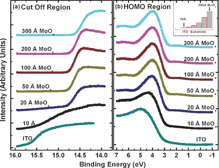 In Fig. 5, the WF versus MoOx interlayer thickness (█) is plotted for 4 Å (•), 8 Å (▴), 32 Å (▾), and 128 Å (⧫) AlPc-Cl coverages. It is simple to deduce the saturation of the WF of the MoOx interlayer at the thickness (█ data points) of 20 Å. At 128-Å AlPc-Cl coverages (⧫), the WF of AlPc-Cl saturates around 4.9 eV, irrespective of MoOx interlayer thickness, representing the saturation of band-bending-like situation in AlPc-Cl. The 32-Å AlPc-Cl coverages have a similar trend, with WF values of <0.2 eV higher than that of the 128-Å coverage. The 4- and 8-Å AlPc-Cl data show clear MoOx interlayer dependence. In the absence of the MoOx interlayer, the variation in WF values is <0.2 eV for all four AlPc-Cl coverages. With increasing interlayer thickness, the WF saturation requires more AlPc-Cl to be deposited. We observed that the BE drop across MoOx interlayer is ∼0.2 eV by AlPc-Cl, regardless of the thickness of the MoOx. The data in Fig. 5 indicate that, for the final 128 Å thickness of AlPc-Cl, there is about the same WF difference from MoOx for interlayer ≥20 Å, but it clearly shows slower relaxation in WF for thicker MoOx interlayer. Because the drift field is the gradient of built-in potential, swifter relaxation results in larger drift field at the interface. This in turn would result in higher hole current. Because of the trade-off between the drift-induced enhancement and increased resistivity of MoOx, 20 Å is most likely the optimum choice of insertion-layer thickness. The prediction of optimum thickness solely on a device-performance basis was recently reported by Cattin et al.,30 which is quite consistent with our UPS results. In Fig. 5, AFM data are presented for 228-Å-thick AlPc-Cl film. The scan area shown is 2 × 2 μm. The root-mean-square (rms) roughness of the film was measured to be 27 Å. Fig. 5(a) Work function versus MoOx interlayer thickness for 4 Å (•), 8 Å (▴), 32 Å (▾) and 128 Å (⧫) AlPc-Cl coverages. (b) AFM data for 2 × 2μm area of 228-Å-thick AlPc-Cl film. 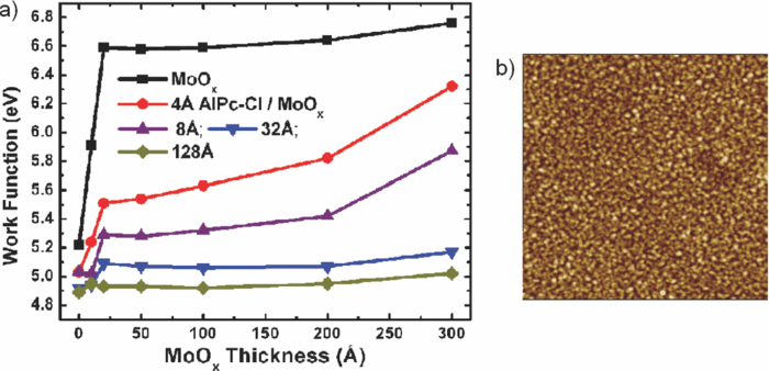 The establishment of the fact that the high WF of the insertion layer is crucial in the uplift of all the frontier energy levels of the organic hole transport layer toward the lower BE at the organic/insertion layer interface raises a question. If the insertion layer surface WF is smaller, then what impact this can have on the device performance? This question needs to be addressed because very recent reports24, 25, 31 have established that the WF of vacuum-grown MoOx film reduces to much lower values after the vacuum is break, which is usually the case with device fabrication. Mayer et al. have reported31 hole-injection properties remain unaffected, while both our OPV24 and OLED25 results—investigated at two different collaborating laboratories—indicate that a vacuum break before the deposition of the organic hole transport layer adversely affects the device performance. In Secs. 3.2 and 3.3, we will discuss the issue of WF reduction due to controlled air and oxygen exposures. 3.3.Effect of Air Exposure to MoOx FilmIn this section, we will address another crucial issue that has been a cause of concern and much debate among experts. The beneficial nature of the MoOx insertion layer is well established, but there were two completely different explanations for this enhancement. The pivotal point in resolving the discrepancy is the WF of MoOx insertion layer. The reported values of WF are in the range of 5.3–6.9 eV.17, 19−23 It is imperative to resolve the discrepancy in order to understand how to control the device fabrication and to obtain consistent device performance. In this section, we report the effect of air exposure to MoOx films. We found that the vacuum-deposited MoOx films started with high initial WF values, but with air exposure, the surface WF gradually reduced to substantially lower values. In Fig. 6, the UPS spectra of the MoOx on ITO are presented as a function of the air exposure. Figures 6 and 6 show the cutoff and valence-band regions of the UPS data, respectively. All the spectra have been normalized to the same height for visual clarity. Short bars are placed at the centroid of MoOx HOMO peaks to track the shift in the peak BE values. The in situ OP-treated ITO WF was measured to be 5.50 eV, which increased to 6.75 eV upon the deposition of 50 Å MoOx. From Fig. 6, a characteristic peak of MoOx can be observed at ∼3.91 eV and HOMO energy-level onset was measured to be 2.69 eV. With air exposure, the surface WF kept continuously decreasing and, at the final step of 2 × 10¹⁴ L exposure, the surface WF was measured to be 5.32 eV, which is 1.44 eV lower than the initial surface WF. The HOMO peak has smaller but continuous shift toward the higher BE, and at the 2 × 10¹⁴ L exposure, the HOMO peak was measured to be 4.33 eV, ∼0.42 eV higher than the initial unexposed value. In Fig. 5, AFM data for 50 Å MoOx film is presented. The scan area shown is 5 × 5 μm. The rms roughness of the film measured was ∼46 Å. Fig. 6UPS data for ITO; 50 Å MoOx; and 102, 104, 106, 108, 1010, 1011, 1012, 5 × 10¹², 1013, 5 × 10¹³, 1014, and 2 × 10¹⁴ L air exposure in (a) the cutoff region and (b) the HOMO region. Substantial to low WF reduction is observed, depending on the amount of air exposure. (c) AFM image of 50-Å MoOx film is presented. 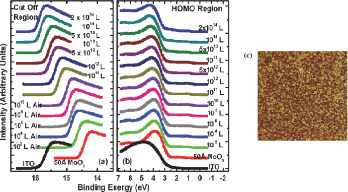 In Fig. 7, the binding-energy evolution of the core levels of Mo 3d5/2 and 3d3/2 [Fig. 7] and O1s [Fig. 7] are presented as a growing amount of air exposure. It is straightforward to conclude that no significant core level peak shift has occurred due to the air exposure. The full width at half the maximum (FWHM) peak height of O 1s peak was 1.8 eV. Not only the peak BE, but also the FWHM remained the same for O 1s core level. The FWHM for Mo 3d 5/2 peak in the beginning was found to be 1.6 eV. With air exposure, however, FWHM for the Mo 3d 5/2 peak kept increasing. At the final 2 × 10¹⁴ L air exposure, it was calculated to be 1.9 eV. The separation between spin-orbit splitting levels Mo 3d5/2 and 3d3/2 is 3.10 eV, which is consistent with reported values in the literature.33 It is interesting to note that the core level positions remain unchanged during the exposure, in contrast to the valence peak shift of 0.42 eV toward higher binding energy. This indicates that the shift is confined to the valence states due to the chemisorption of the gas molecules. Fig. 7XPS data for, (a) the Mo 3d and (b) the O 1s core level for, ITO, 50 Å MoOx, and 102, 104, 106, 108, 1010, 1011, 1012, 5 × 10¹², 1013, 5 × 10¹³, 1014, and 2 × 10¹⁴ L air exposure. 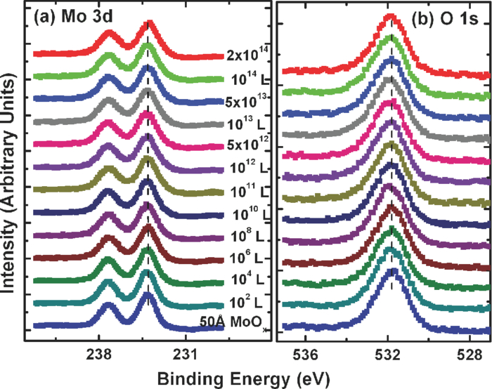 In Fig. 8, the growth of a gap state near the Fermi energy level is shown as a function of air exposure. The broad peak at ∼2.0 eV is a satellite of the HOMO from the He β line at 23.09 eV from our unfiltered He I (21.22 eV) ultraviolet photon source.33 With the air exposure, the gap state at ∼1.1 eV grows. The gap-state peak is clearly visible from 104 L onward, which becomes more prominent with further air exposure. It can be understood that the electron transfer from the adsorbates to MoOx dopes the latter at the surface, and as a result, the HOMO of MoO3 shifts downward by 0.43 eV, as shown in Fig. 6. From Fig. 8, it is clear that the gap state is not intrinsic to the MoOx but originates from electron transfer from adsorbates sticking to the MoOx film at the surface. The effect of this gap state on device performance has not been determined. 3.4.Effect of Oxygen Exposure to MoOx FilmAfter establishing the WF reduction of MoOx film on exposure to air and resolving the discrepancies in the reported MoOx WF values in the literature, in this section we will discuss the effect of oxygen exposure on MoOx films. An oxygen exposure experiment along with the previous air exposure experiment would allow us to decouple the effect of oxygen molecules and humidity on the surface of MoOx film. We found that the vacuum-deposited MoOx film started with high initial WF values, but with oxygen exposure, the surface WF gradually reduced to substantially lower values, but the near saturation of the WF was observed higher than the air-exposed MoOx films. In Fig. 9, the energy-level evolution of 50-Å MoOx film on ITO are presented as an increasing amount of oxygen exposure. The cutoff and valence-band regions of the UPS data are presented in Figs.9 and 9, respectively. All the spectra have been normalized to the same height for visual clarity. Short bars are placed at the centroid of MoOx HOMO peaks to track the shift in the peak BE values. The in situ OP-treated ITO WF was found to be 5.58 eV. The deposition of 50 Å MoOx lead to a high increment of 1.16 eV in the surface WF. From Fig. 9, a characteristic peak of MoOx can be observed at ∼3.9 eV and HOMO energy-level onset was measured to be 2.66 eV. With oxygen exposure, a continuous surface WF reduction was observed, which saturated around ≥1013 L oxygen exposure. At the final step of 5 × 10¹⁴ L exposure, the surface WF was measured to be 5.75 eV, which is 1 eV lower than the initial MoOx surface WF. The HOMO peak as well has smaller but continuous shift towards the higher BE, and at the 5 × 10¹⁴ L oxygen exposure, the HOMO peak was measured to be 4.04 eV. With the oxygen exposure, the surface WF kept continuously decreasing in a similar fashion as in the air exposure experiment except for exposures of >1014 L. Fig. 9Electronic energy-level evolution of oxygen-exposed MoOx film. The UPS data presented is for ITO, 50 Å MoOx, and 1, 102, 104, 106, 108, 1010, 1011, 1012, 5 × 10¹², 5 × 10¹³, and 5 × 10¹⁴ L oxygen exposure (a) the cutoff region and (b) the HOMO region. Continuous reduction in surface WF is demonstrated. 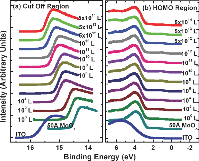 In Fig. 10, the core energy-level evolution of (a) Mo 3d5/2 and 3d3/2, and (b) O1s are exhibited as a growing amount of oxygen exposure. Once again, there was no appreciable shift in the peak binding position of both Mo 3d and O 1s core levels. No significant peak broadening was observed in O 1s core levels from the initial thermally evaporated value of 1.78 eV. However, some peak broadening was again observed in Mo 3d5/2 peak. The initial FWHM for Mo 3d5/2 peak was 1.63 eV, which became 2.00 eV for 5 × 10¹² L oxygen exposure. The separation between spin-orbit splitting levels Mo 3d5/2 and 3d3/2 were 3.10 eV, which is consistent with reported values in the literature.32 Fig. 10Core energy-level evolution of MoOx film. XPS data for, (a) the Mo 3d and (b) the O 1s core level for, ITO, 50 Å MoOx, and 1, 102, 104, 106, 108, 1010, 1011, 1012, 5 × 10¹², 5 × 10¹³, and 5 × 10¹⁴ L oxygen exposure. 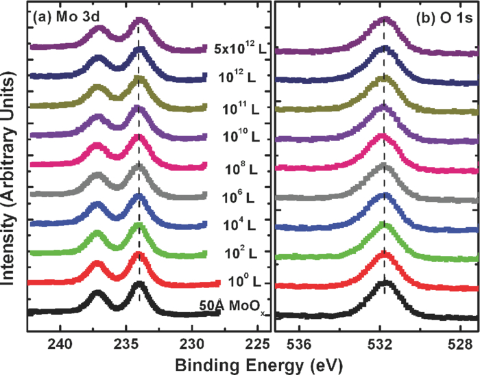 In Fig. 11, the growth of a gap state close to the Fermi energy level is shown as a function of oxygen exposure. The growth of a gap state at ∼1.1 eV is observed with the oxygen exposure. The gap-state peak is clearly visible from 104 L onward, which becomes more prominent with further air exposure. Nakayama et al. reported a similar interface electronic state at ∼1 eV on initial deposition of MoOx on poly(dioctylfluorine-alt-benzothiadiazole) (F8BT), which attenuated after 23 Å of MoOx.34 Our data in Fig. 3 suggest that the gap state observed by Nakayama et al.34 is from electron transfer from F8BT to MoOx. At present, it is not clear what effects this gap state has on the device performance. It is also interesting to note that Kroger et al. meticulously ruled out the existence of a gap state in MoOx.20, 23 Our results indicate that the gap state indeed is not intrinsic to MoOx. Instead, it is by charge transfer to MoOx at the interface from interaction with other materials. Fig. 11Near HOMO region UPS data in situ OP-treated ITO, 50 Å MoOx, and 1, 102, 104, 106, 108, 1010, 5 × 10¹², and 5 × 10¹⁴ L oxygen exposure. The growth of gap state at ∼1.1 is clearly visible. 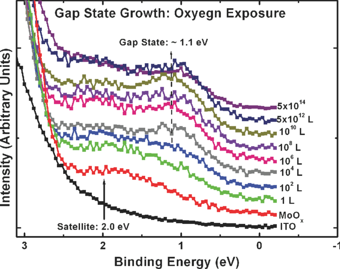 The reduction in the WF and growth of the gap state are consistent to a physical model of electron transfer from chemisorbed oxygen to MoOx, forming an interface dipole layer pointing toward the MoOx surface. Because the oxygen ionization potential is high (12.063 eV),35 the dielectric screening by the MoOx has to be included to facilitate such a charge transfer.36 Below a ≤1013-L exposure charge transfer from an oxygen molecule seems to be the dominant mechanism. Beyond 1013 L of air exposure, the reduction of the work function is most likely from the polarization of the adsorbed water molecule because the gap-state intensity no longer increases at this stage, as shown in Fig. 11. The UPS and XPS studies illustrated the evolution of the electronic structure of the MoOx during the interface formation with organic materials and with exposure to oxygen or air. It can be concluded that the high WF of MoOx is the dominant factor that brings the HOMO level of the organic toward the Fermi level of the anode and creates a band-bending-like region that encourages holes to drift toward the anode. The reduction of WF by gas exposure can be clearly correlated to the deteriorating device performance.21 The low LUMO energy of MoOx should also be an important factor contributing to the carrier transport.20 However, its significance is secondary in comparison to the WF as the gas exposure brings the frontier orbitals even lower by ∼0.4 eV while the device performance is deteriorated.21 It can also be concluded that the gap state is associated with the electron doping of MoOx by organic materials or other adsorbates. It grows and saturates at high gas exposures, opposite to the trend of the device performance. It therefore remains questionable how much the gap state contributes to improvement of the device performance. 4.ConclusionsIn conclusion, we have measured the electronic structure evolution of interfaces with 0–300 Å stepped MoOx interlayers between ITO and AlPc-Cl. We observed that the high work function of the metal oxide interlayer pulls up the energy levels of AlPc-Cl toward lower binding energy at the interface, resulting in band-bending-like situation in the organic material. For thermally evaporated MoOx, it takes 20 Å MoOx for the work function to saturate. We observed ∼0.2 eV voltage drop across MoOx as AlPc-Cl is deposited. We postulate that the band-bending-like phenomenon in AlPc-Cl introduces a drift electric field inside the organic hole transport layer. This built-in drift field enhances hole extraction to the ITO and thus reducing the series resistance, which is the main contributing factor for the efficiency enhancement of devices with MoOx interlayer. Additionally, we have measured the electronic structure evolution of air and oxygen-exposed 50 Å MoOx/ITO film. We observed the HOMO level of MoOx is largely intact beside work function ∼6.75 eV from thermally evaporated MoOx films. We found that, with increasing air exposure, the surface work function gradually drops down and nearly saturated at 5.35 eV for the air exposure of 2 × 10¹⁴ L. An almost similar WF descend trend was observed in oxygen-exposed MoOx film, and saturation was observed for O2 exposure ∼1014 L, and at 5 × 10¹⁴ L oxygen exposure, the surface work function was found to be 5.75 eV. In both the air and oxygen-exposed MoOx films, we observed growth of an interface gap state at the binding energy of ∼1.1 eV with increasing exposure, and a 0.43-eV shift of the HOMO peak toward higher BE in the air-exposure experiment. The work-function reduction is dominated by the oxygen adsorption at the surface for ≤1013-L exposure, and beyond that, moisture absorption seems to be a dominant mechanism in the reduction of the surface work function. We have previously reported that hole-extraction enhancement in organic solar cells is due to the high MoOx work function.21 It is crucial to avoid oxygen and moisture exposure to the thermally evaporated MoOx films in order to preserve the enhancement. AcknowledgmentThe authors at UR acknowledge the support of the National Science Foundation Grant No. DMR-1006098. F.S. acknowledges the support of the Florida Energy Systems Consortium. ReferencesC. W. Tang,
“Two-layer organic photovoltaic cell,”
Appl. Phys. Lett., 48 183
–185
(1986). http://dx.doi.org/10.1063/1.96937 Google Scholar
G. Yu, J. Gao, J. C. Hummelen, F. Wudl, and A. J. Heager,
“Polymer photovoltaic cells: enhanced efficiencies via a network of internal donor-acceptor heterojunctions,”
Science, 270 1789
–1791
(1995). http://dx.doi.org/10.1126/science.270.5243.1789 Google Scholar
P. Peumans and S. R. Forrest,
“Very-high-efficiency double-heterostructure copper phthalocyanine/C60 photovoltaic cells,”
Appl. Phys. Lett., 79 126
–128
(2001). http://dx.doi.org/10.1063/1.1384001 Google Scholar
J. Xue, S. Uchida, B. P. Rand, and S. R. Forrest,
“4.2% efficient organic photovoltaic cells with low series resistances,”
Appl. Phys. Lett., 84 3013
–3015
(2004). http://dx.doi.org/10.1063/1.1713036 Google Scholar
G. Li, V. Shrotriya, J. Huang, Y. Yao, T. Moriarty, K. Emery, and Y. Yang,
“High-efficiency solution processable polymer photovoltaic cells by self-organization of polymer blends,”
Nat. Mater., 4 864
–868
(2005). http://dx.doi.org/10.1038/nmat1500 Google Scholar
C. W. Tang and S. A. Vanslyke,
“Organic electroluminescent diodes,”
Appl. Phys. Lett., 51 913
–915
(1987). http://dx.doi.org/10.1063/1.98799 Google Scholar
R. H. Friend, R. W. Gymer, A. B. Holmes, J. H. Burroughes, R. N. Marks, C. Taliani, D. D. C. Bradley, D. A. Dos Santos, J. L. Bredas, M. Logdlund, and W. R. Salaneck,
“Electroluminescence in conjugated polymers,”
Nature, 397 121
–128
(1999). http://dx.doi.org/10.1038/16393 Google Scholar
S. J. Su, E. Gonmori, H. Sasabe, and J. Kido,
“Highly efficient organic blue-and white-light-emitting devices having a carrier and exciton confining structure for reduced efficiency roll-off,”
Adv. Mater., 20 4189
–4195
(2008). http://dx.doi.org/10.1002/adma.200801375 Google Scholar
G. Horowitz,
“Organic field-effect transistors,”
Adv. Mater., 10 365
–377
(1998). http://dx.doi.org/10.1002/(SICI)1521-4095(199803)10:5365::AID-ADMA3653.0.CO;2-U Google Scholar
C. D. Dimitrakopoulos and D. J. Mascaro,
“Organic thin-film transistors: a review of recent advances,”
IBM J. Res. Dev., 45 11
–27
(2001). http://dx.doi.org/10.1147/rd.451.0011 Google Scholar
Z. H. Xiong, D. Wu, Z. V. Vardeny, and Z. Shi,
“Giant magnetoresistance in organic spin-valves,”
Nature, 427 821
–824
(2004). http://dx.doi.org/10.1038/nature02325 Google Scholar
M. Cinchetti, K. Heimer, J. P. Wüstenberg, O. Andreyev, M. Bauer, S. Lach, C. Ziegler, Y. Gao, and M. Aeschlimann,
“Determination of spin injection and transport in a ferromagnet/organic semiconductor heterojunction by two-photon photoemission,”
Nat. Mater., 8 115
–119
(2009). http://dx.doi.org/10.1038/nmat2334 Google Scholar
C. J. Brabec,
“Organic photovoltaics: technology and market,”
Sol. Energy Mater. Sol. Cells, 83 273
–292
(2004). http://dx.doi.org/10.1016/j.solmat.2004.02.030 Google Scholar
S. Tokito, K. Noda, and Y. Taga,
“Metal oxides as a hole-injecting layer for an organic electroluminescent device,”
J. Phys. D, 29 2750
–2753
(1996). http://dx.doi.org/10.1088/0022-3727/29/11/004 Google Scholar
F. X. Wang, X. F. Qiao, T. Xiong, and D. G. Ma,
“The role of molybdenum oxide as anode interfacial modification in the improvement of efficiency and stability in organic light-emitting diodes,”
Org. Electron., 9 985
–993
(2008). http://dx.doi.org/10.1016/j.orgel.2008.07.009 Google Scholar
S. Reineke, F. Linder, G. Schwartz, N. Seidler, K. Walzer, B. Lussem, and K. Leo,
“White organic light-emitting diodes with fluorescent tube efficiency,”
Nature, 459 234
–238
(2009). http://dx.doi.org/10.1038/nature08003 Google Scholar
V. Shrotriya, G. Li, Y. Yao, C. W. Chu, and Y. Yang,
“Transition metal oxides as the buffer layer for polymer photovoltaic cells,”
Appl. Phys. Lett., 88 073508
(2006). http://dx.doi.org/10.1063/1.2174093 Google Scholar
M. D. Irwin, D. B. Buchholz, A. W. Hains, R. P. H. Chang, and T. J. Marks,
“p-Type semiconducting nickel oxide as an efficiency-enhancing anode interfacial layer in polymer bulk-heterojunction solar cells,”
Proc. Natl. Acad. Sci. U.S.A., 105 2783
–2787
(2008). http://dx.doi.org/10.1073/pnas.0711990105 Google Scholar
D. Y. Kim, J. Subbiah, G. Sarasqueta, F. So, H. Ding, Irfan, and Y. Gao,
“The effect of molybdenum oxide interlayer on organic photovoltaic cells,”
Appl. Phys. Lett., 95 093304
(2009). http://dx.doi.org/10.1063/1.3220064 Google Scholar
M. Kroger, S. Hamwi, J. Meyer, T. Riedl, W. Kowlasky, and A. Kahn,
“Role of deep lying electronic states of MoO3 in the enhancement of hole-injection in organic thin films,”
Appl. Phys. Lett., 95 123301
(2009). http://dx.doi.org/10.1063/1.3231928 Google Scholar
Irfan, H. Ding, Y. Gao, D. Y. Kim, J. Subbiah, and F. So,
“Energy level evolution of molybdenum trioxide interlayer between indium tin oxide and organic semiconductor,”
Appl. Phys. Lett., 96 0733041
(2010). http://dx.doi.org/10.1063/1.3309600 Google Scholar
T. Matasushima, Y. Kinoshita, and H. Murata,
“Formation of ohmic hole injection by inserting an ultrathin layer of molybdenum trioxide between indium tin oxide and organic hole-transporting layers,”
Appl. Phys. Lett., 91 253504
(2007). http://dx.doi.org/10.1063/1.2825275 Google Scholar
M. Kroger, S. Hamwi, J. Meyer, T. Riedl, W. Kowlasky, and A. Kahn,
“P-type doping of organic wide band gap materials by transition metal oxides: a case study on molybdenum trioxide,”
Org. Electron., 10 932
–938
(2009). http://dx.doi.org/10.1016/j.orgel.2009.05.007 Google Scholar
M. Zhang, Irfan, H. Ding, Y. Gao, and C. W. Tang,
“Organic Schottky barrier photovoltaic cells based on MoOx/C60,”
Appl. Phys. Lett., 96 183301
(2010). http://dx.doi.org/10.1063/1.3415497 Google Scholar
Irfan, H. Ding, Y. Gao, D. Y. Kim, J. Subbiah, C. Small, and F. So,
“Energy level evolution of air and oxygen exposed molybdenum trioxide films,”
Appl. Phys. Lett., 96 243307
(2010). http://dx.doi.org/10.1063/1.3454779 Google Scholar
X. M. Ding, L. H. Hung, L. F. Cheng, X. Y. Hou, C. S. Lee, and S. T. Lee,
“Modification of the hole injection barrier in organic light emitting devices by ultraviolet photoelectron spectroscopy,”
Appl. Phys. Lett., 76 2704
–2706
(2000). http://dx.doi.org/10.1063/1.126449 Google Scholar
Y. Park, Y. Choong, Y. Gao, B. R. Hsieh, and C. W. Tang,
“Work function of indium tin oxide transparent conductor measured by photoelectron spectroscopy,”
Appl. Phys. Lett., 68 2699
–2701
(1996). http://dx.doi.org/10.1063/1.116313 Google Scholar
J. Huang, A. Wan, and A. Khan,
“Energetics of metal-organic interfaces: New experiments and assessment of the field,”
Mater. Sci. Eng. Res., 64 1
–31
(2009). http://dx.doi.org/10.1016/j.mser.2008.12.001 Google Scholar
Y. Gao,
“Surface analytical studies of interfaces in organic semiconductor devices,”
Mater. Sci. Eng. Res., 68 39
–87
(2010). http://dx.doi.org/10.1016/j.mser.2010.01.001 Google Scholar
L. Cattin, F. Dahou, Y. Lare, M. Morsli, R. Tricot, S. Houari, A. Mokrani, K. Jondo, A. Khelil, K. Napo, and J. C. Bernede, J. Appl. Phys., 105 034507
(2009). http://dx.doi.org/10.1063/1.3077160 Google Scholar
J. Mayer, A. Shu, M. Kroger, and A. Khan,
“Effect of contamination on the electronic structure and hole-injection properties of MoO3/organic semiconductor interfaces,”
Appl. Phys. Lett., 96 133308
(2010). http://dx.doi.org/10.1063/1.3374333 Google Scholar
F. Werfel and E. Minni,
“Photoemission study of the electronic structure of Mo and Mo oxides,”
J. Phys. C, 16 6091
–6100
(1983). http://dx.doi.org/10.1088/0022-3719/16/31/022 Google Scholar
J. B. Peel and E. I. V. Felsobuki,
“The far ultraviolet emission of a helium discharge source studied by photoelectron spectroscopy,”
J. Chem. Educ., 64 463
–466
(1987). http://dx.doi.org/10.1021/ed064p463 Google Scholar
Y. Nakayama, K. Morii, Y. Suzuki, H. Mashida, S. Kera, N. Ueno, H. Kitagawa, Y. Noguchi, and H. Ishii,
“Origins of improved hole-injection efficiency by the deposition of MoO3 on the polymeric semiconductor poly(dioctylfluorene-alt-benzothiadiazole),”
Adv. Func. Mater., 19 3746
–3752
(2009). Google Scholar
R. C. Weast, Handbook of Chemistry and Physics, Chemical Rubber, Cleveland
(1970). Google Scholar
M. Sayer, A. Mansingh, J. B. Webb, and J. Noad,
“Long-range potential centres in disordered solids,”
J. Phys. C, 11 315
–329
(1978). http://dx.doi.org/10.1088/0022-3719/11/2/016 Google Scholar
BiographyIrfan is a PhD candidate in the Department of Physics and Astronomy at the University of Rochester under the supervision of Professor Yongli Gao. In 2004, he received a BS from the University of Lucknow. He received his MS in physics in 2006 from S. N. Bose National Institute for basic Sciences, Kolkata, India. He joined the University of Rochester in 2007 and is currently studying electronic structure and energy-level alignment at metallorganic semiconductor, metal/oxide/organic semiconductor interfaces. These studies are helpful in understanding and predicting device performances of OLED and OPV cell. His current work focuses on the role of molybdenum tri-oxide insertion layers at the anode of organic semiconductor devices. Huanjun Ding attended Shandong University in China from 1996 to 2000 and graduated with a BS in Physics. After that, he continued his graduate studies in physics at Fudan University in Shanghai, China, where he received a MS in physics in 2003. He arrived at the Department of Physics and Astronomy at the University of Rochester in 2003 to pursue further education. He studied the electronic structures of organic semiconductors under the supervision of Professor Yongli Gao and received his PhD in 2010. Franky So is a professor in the Department of Materials Science and Engineering at the University of Florida. He received his PhD in electrical engineering from the University of Southern California. After graduation in 1991, he was a research scientist at Hoechst Celanese Research Division, working on polymer electro-optical modulators and OLEDs. In 1993, he joined Motorola Phoenix Corporate Laboratories working on OLEDs for flat-panel displays. In 2001, he joined OSRAM Opto Semiconductors and then became the head of OLED Research. He is a Fellow of SPIE and an associate editor of IEEE Journal of Display Technology, SPIE Journal of Photonics for Energy, and Materials Science and Engineering Reports. He has over 60 publications, 52 issued patents, and another 20 patent applications pending. Yongli Gao received his BS in physics from Central-South Institute of Mining and Metallurgy, China in 1981, and PhD in physics from Purdue University in 1986 under the guidance of Professor Ron Reifenberger. From 1986 to 1988, he was a postdoctoral fellow with Professor John Weaver at University of Minnesota. He joined the faculty of the University of Rochester in 1988 and was promoted to associate professor and full professor in physics in 1994 and 1999, respectively. He has published over 200 papers on interface formation in organic semiconductors, ultrafast electronic dynamics in metals, semiconductors, and quantum wells, surface stability and interface formation of high Tc superconductors, low-temperature Schottky barrier formation and dielectric layer formation on III–V semiconductors, surface melting, and mechanisms of x-ray photoelectron and Auger electron diffraction. |