|
|
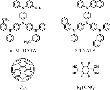
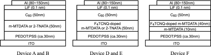
1.IntroductionOrganic thin-film photovoltaic (OPV) devices have been receiving a great deal of attention as candidates for next-generation solar cells or photodetectors because of their potentially low cost, light weight, and capability of large-area, flexible device fabrication.1, 2, 3, 4, 5 The development of new materials, including both small molecules and polymers, and the implementation of new device structures have led to significant improvement in power conversion efficiency (PCE).6, 7, 8, 9, 10, 11, 12, 13, 14, 15, 16, 17, 18 At present, PCEs of 8% under simulated sunlight illumination have been attained.19, 20, 21 With regard to small molecular materials for OPV devices, polycrystalline materials have usually been used because of their relatively high charge-carrier mobilities. Phthalocyanines, and perylene pigments and fullerenes are typical examples of electron donors and acceptors that give a high PCE. Recently, growing attention has also been paid to amorphous molecular materials for use in OPV devices. Following the report that a planar pn-heterojunction OPV device using N,N′-bis(α-naphthyl)-N,N′-diphenyl-[1,1′-biphenyl]-4,4′-diamine as an electron donor and C60 as an electron acceptor exhibits 1% PCE,22 there have been extensive studies on OPV devices using a variety of amorphous molecular materials as electron donors and fullerenes as electron acceptors, and a PCE up to over 2% has been attained.23, 24, 25, 26, 27, 28, 29, 30, 31, 32, 33, 34, 35, 36 With regard to device structures, p-i-n,7, 12, 14 bulk-heterojunction,6, 8 and tandem structures,11, 13, 17 as well as a planar pn-heterojunction structure, together with the incorporation of an exciton-blocking layer9, 10, 16 or optical spacers,15, 16 have been employed to improve the PCE. Unlike inorganic semiconductors, organic semiconductors that are used for OPV devices are essentially insulators. The observed current density that flows in the external circuit of OPV devices at given cell voltages under simulated sunlight illumination significantly decreases as the series resistance in the equivalent circuit increases; this results in a low fill factor (FF) and PCE. Making organic layers as thin as possible and reducing the contact resistance at the interface between organic layers and electrodes are required to improve the PCE of OPV devices. Charge-transfer doping of organic layers is an effective method for reducing the series resistance in the equivalent circuit. It is well known that charge-transfer doping, i.e., p- or n-type doping, of both π-conjugated polymers,37, 38 and polymers containing pendant π-electron systems39 produces electrically conducting polymers. Electrochemically p-doped pendant polymers40, 41 and chemically doped polymers42 have been used as materials for OPV devices and organic light-emitting diodes (OLEDs). Recently, charge-transfer doping has been extended to amorphous molecular materials,43 and p- or n-doped crystalline and amorphous molecular materials have been applied for OPV devices and OLEDs.12, 44, 45, 46, 47, 48 It has been shown that p-doping of zinc phthalocyanine and amorphous molecular materials, e.g., 4,4′,4″-tris[3-methylphenyl(phenyl)amino]triphenylamine (m-MTDATA) and 4,4′,4″-tris(diphenylamino)triphenylamine (TDATA), with 2,3,5,6-tetrafluoro-7,7,8,8-tetracyanoquinodimethane (F4TCNQ) increases the electrical conductivities of these organic materials;12, 44, 45, 46, 47, 48 as a result, hole injection from the electrode is enhanced in OLEDs, and the operating voltage is significantly reduced.45, 46, 47, 48 With regard to OPV devices, it has not been fully clarified how charge-transfer doping affects device performance parameters such as open-circuit voltage (VOC), short-circuit current density (JSC), and FF. In the present study, we have investigated the effect of p-type doping of the donor layer with F4TCNQ on the performance of planar pn-heterojunction OPV devices. Amorphous molecular materials with low solid state ionization potentials (Ips), m-MTDATA (Ip 5.1 eV,49) and 4,4′,4″-tris[2-naphthyl(phenyl)amino]triphenylamine (2-TNATA) (Ip 5.15 eV50), and C60 were used as electron donors and an electron acceptor, respectively. These electron donors with the low solid-state ionization potentials are thought to be suitable for p-type doping, enabling electron transfer to an electron acceptor, F4TCNQ, in the ground state. In addition, grain-boundary-free amorphous molecular materials that form smooth, uniform amorphous thin films are expected to allow uniform doping.51, 52 2.Experimental2.1.Materialsm-MTDATA,53 2-TNATA,50 and N,N’-bis(3-methylphenyl)-diphenyl-[1,1′-biphenyl]-4,4′-diamine (TPD) were purchased from OHJEC Co. C60 was purchased from Nakalai Tesque, Inc. F4TCNQ was purchased from Wako Pure Chemical Industries, Ltd. Indium-tin-oxide (ITO)-coated glass with a sheet resistance of 15 Ω / □ was purchased from Sanyo Vacuum Industries, Co., Ltd. 2.2.Device FabricationITO-coated glass substrates were cleaned by successive washing with neutral detergent, deionized water, tetrahydrofuran (THF), and trichloroethene in an ultrasonic bath, followed by exposure to trichloroethene vapor. Finally, the substrates were irradiated with ultraviolet light (Senjyu UV lamp VX-200HK002) for 20 min. Poly(3,4-ethylenedioxythiophene) doped with poly(4-styrene sulfonate) (PEDOT:PSS) (H. C. Starck, PH500) was spin-coated onto the ITO-coated glass substrate with a spin coater (ASS 302; 3000 rpm, 10 s), and then dried at 130ºC for 10 min. Amorphous thin films of m-MTDATA or 2-TNATA were prepared by a thermal deposition method onto the PEDOT:PSS layer at 2.6×10⁻⁴ Pa at a deposition rate of 0.1 nm s−1 at room temperature. Then, C60 was vacuum deposited onto the m-MTDATA or 2-TNATA film at 2.6×10⁻⁴ Pa at a deposition rate of 0.1 nm s−1 at room temperature, followed by successive thermal deposition of lithium fluoride (0.02 nm s−1 ) and aluminum (0.4 to 0.8 nm s−1) onto the C60 layer. Doping of m-MTDATA or 2-TNATA with F4TCNQ was carried out by co-deposition of m-MTDATA or 2-TNATA and F4TCNQ at 2.6×10⁻⁴ Pa at a deposition rate ratio of 10:1. The fabricated devices were sealed using glass plates with epoxy resin in a nitrogen-filled glove box and then annealed at 100ºC for 10 min before measurements. 2.3.MeasurementsCurrent density – voltage characteristics in the dark and under AM1.5G illumination (500 W Xenon lamp, USHIO UXL-500SX, AM1.5 filter) at room temperature were recorded using an Advantest R6243 power source meter. Light intensity was measured using a power meter (MELLES GRIOT, Broadband Power/Energy Meter, 13PEM 001). 3.Results and Discussionm-MTDATA and TDATA doped with F4TCNQ have been used as a hole-transporting layer in OPV devices;13, 45, 46 however, the performance data of planar pn-heterojunction OPV devices using m-MTDATA as an electron donor and C60 as an electron acceptor is not yet available in the literature. In the present study, planar pn-heterojunction OPV devices consisting of m-MTDATA or 2-TNATA as an electron donor and C60 as an electron acceptor, ITO/PEDOT:PSS (ca. 30 nm)/m-MTDATA (50 nm)/C60 (50 nm)/LiF (0.1 nm)/Al (80 to 150 nm) (device A) and ITO/PEDOT:PSS (ca. 30 nm)/2-TNATA (50 nm)/C60 (50 nm)/LiF (0.1 nm)/Al (80 to 150 nm) (device B), were fabricated, and their performance was examined. Then, the effect of p-type doping of the donor layer with F4TCNQ on the cell performance was investigated. For this purpose, the following devices were fabricated: ITO/PEDOT:PSS (ca. 30 nm)/m-TDATA: F4TCNQ (10:1.0) (50 nm)/C60 (50 nm)/LiF (0.1 nm)/Al (80 to 150 nm) (device D) and ITO/PEDOT:PSS (ca. 30 nm)/2-TNATA :F4TCNQ (10:1.0) (50 nm)/C60 (50 nm)/LiF (0.1 nm)/Al (80 to 150 nm) (device E). Figure 1 shows the structures of the fabricated OPV devices. Figures 2 and 2 show the current density (J) − voltage (V) characteristics of device A and device D, and device B and device E, respectively, in the dark and under AM1.5G illumination at an incident light intensity of 100 mW cm−2. Table 1 summarizes the performance of the fabricated OPV devices, VOC, JSC, FF, and PCE, under AM1.5G illumination at an incident light intensity of 100 mW cm−2. Device A using m-MTDATA as an electron donor exhibited a VOC of 0.40 V, a JSC of 0.7 mA cm−2, a FF of 0.24, and a PCE of 0.07%. Device B using 2-TNATA as an electron donor showed similar performance to that of device A, exhibiting a VOC of 0.45 V, a JSC of 0.5 mA cm−2, a FF of 0.25, and a PCE of 0.05%. For comparison, a corresponding pn-heterojunction device using TPD as an electron donor and C60 as an electron acceptor, ITO/PEDOT:PSS (ca. 30 nm)/TPD (50 nm)/C60 (50 nm)/LiF (0.1 nm)/Al (80 to 150 nm) (device C), was also fabricated and its performance was examined. Device C exhibited a VOC of 0.67, a JSC of 1.4 mA cm−2, a FF of 0.42, and a PCE of 0.38% (Table 1). Table 1Device performance under AM1.5G illumination at an intensity of 100 mW cm−2.
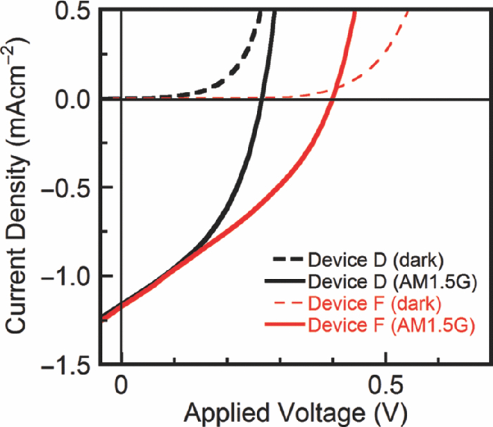
Device A : ITO/PEDOT:PSS (ca. 30 nm)/m-MTDATA (50 nm)/C60 (50 nm)/LiF (0.1 nm)/Al (80 to 150 nm). Device B : ITO/PEDOT:PSS (ca. 30 nm)/ 2-TNATA (50 nm)/C60 (50 nm)/LiF (0.1 nm)/Al (80 to 150 nm). Device C : ITO/PEDOT:PSS (ca. 30 nm)/TPD (50 nm)/C60 (50 nm)/LiF (0.1 nm)/Al (80 to 150 nm). Device D : ITO/PEDOT:PSS (ca. 30 nm)/F4TCNQ-doped m-MTDATA (50 nm)/C60 (50 nm)/LiF (0.1 nm)/Al (80 to 150 nm). Device E : ITO/PEDOT:PSS (ca. 30 nm)/F4TCNQ-doped 2-TNATA (50 nm)/C60 (50 nm)/LiF (0.1 nm)/Al (80 to 150 nm). Device F : ITO/PEDOT:PSS (ca. 30 nm)/m-MTDATA (10 nm)/F4TCNQ-doped m-MTDATA (40 nm)/C60 (50 nm)/LiF (0.1 nm)/Al (80 to 150 nm). All devices were annealed at 100ºC for 10 min. Fig. 2J–V characteristics of (a) device A and device D, and (b) device B and device E in the dark and under AM1.5G illumination at an incident light intensity of 100 mW cm−2. 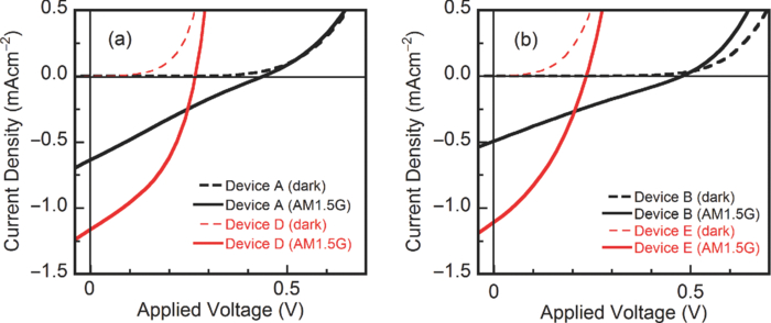 It has generally been understood that VOC corresponds to the difference between the highest occupied molecular orbital (HOMO) level of electron donor and the lowest unoccupied molecular orbital (LUMO) level of electron acceptor.4 The VOC values from 0.40 to 0.45 V observed for device A and device B roughly correspond to the difference between the HOMO level of m-MTDATA or 2-TNATA (5.1, 5.15 eV)5, 49, 50 and the LUMO level of C60 (4.5 eV).2 Likewise, the VOC value of 0.67 V observed for device C roughly corresponds to the difference between the HOMO level of TPD (5.45 eV)50 and the LUMO level of C60. Since m-MTDATA and 2-TNATA have similar solid-state ionization potentials and hole drift mobilities of ∼3 × 10⁻⁵ cm2 V−1s−1 at 1.0 × 10⁵ V m−1 at room temperature,54, 55, 56, 57 the similar performance observed for device A and device B seems to be reasonable. As light is mainly absorbed by C60, slight differences in the ultraviolet absorption spectra between m-MTDATA and 2-TNATA did not appreciably affect the performance under simulated AM 1.5G sunlight illumination. Very low PCEs of these devices stem from relatively low VOC and small JSC and FF. The relatively low VOC is attributed to the low HOMO levels of these electron donors, and the small JSC value is attributed to the absence of visible light absorption by m-MTDATA and 2-TNATA (Fig. 3) and to their very low hole drift mobilities. It has been reported that the dissociation process of photogenerated hole-electron pairs at the donor/acceptor interface to generate charge carriers in competition with the charge recombination process is greatly influenced by charge-carrier mobilities of organic materials used and that a tenfold increase in mobility dramatically improves JSC and FF, doubling the maximum power output.58 The limited FF for these devices results from the large series resistance (Rs) of these devices. In fact, the Rs values calculated from the J−V curves under illumination were ca. 210 and 60 Ωcm2 for device A and device B, respectively. The relatively small shunt resistance (Rsh) values under illumination (ca. 650 and 1200 Ωcm2 for device A and B) were also thought to be responsible for the low FF. Higher performance of device C than that of device A and device B is attributable to the higher HOMO level and much higher hole drift mobility of TPD (1.0 × 10⁻³ cm2 V−1 s−1 at 1.0 × 10⁵ V cm−1)57 relative to those of m-MTDATA and 2-TNATA. Fig. 3Electronic absorption spectra of vapor-deposited films of m-MTDATA (30 nm) and 2-TNATA (30 nm). 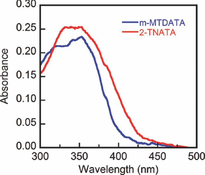 The p-doping of the donor layer with F4TCNQ resulted in the increase of both JSC and FF and a significant decrease of VOC. That is, device D and device E exhibited 1.7 to 2.0 times higher JSC and 1.5 to 1.6 times larger FF, respectively, but significantly lower VOC than device A and device B. As a result, device D and device E using F4TCNQ-doped materials gave 1.6 to 1.7 times larger PCEs than device A and device B, as shown in Fig. 2 and Table 1. The increase of both JSC and FF caused by the p-doping of the donor layer with F4TCNQ can be explained in terms of the increased hole mobility of F4TCNQ-doped m-MTDATA and 2-TNATA and the decreased series resistance of the devices using these doped donor materials. The increase of charge-carrier mobility by p-type doping has been reported with regard to 1,3,5-tris[N,N-bis(4,5-dimethoxyphenyl)aminophenyl]benzene59 and zinc phthalocyanine.60 The decrease in the resistance of donor materials by p-type doping was shown by the analysis of the J−V curves of device D and device E under illumination. The Rs values calculated from the J−V curves under illumination for device D and device E were ca. 8 and 7 Ω cm2, respectively, which are much smaller than those calculated from the J−V curves of device A and device B using undoped electron donors. The increase in electrical conductivities of m-MTDATA and TDATA by the p-doping with F4TCNQ has been reported.45, 46 The observed current density (Jobs) that flows in the external circuit of OPV devices is given by the subtraction of the photocurrent density (Jph) from the dark current density (Jd) [Eq. 1]. Since JSC is the current density observed at the zero cell voltage where Jd is zero, JSC is equal to Jph. If it is simply assumed that the photocurrent observed for the OPV device corresponds to that observed for photoconductors, Jph is expressed as Eq. 2, where L is the thickness of the sample, I0 is the total number of photons arriving at the unit surface area of the cell per second, α is the absorption coefficient, η is the photogeneration efficiency of charge carriers, τ is the carrier lifetime, e is the elementary electric charge, μ is the charge carrier mobility, and E is the electric field. The parameters involved in Jph that are affected by the p-doping of the electron donor are suggested to be μ and η. That is, the increase in Jph is attributable to the increase of μ for the p-doped donor materials and to the increase of η owing to the increased μ. [TeX:] \documentclass[12pt]{minimal}\begin{document}\begin{equation}
J_{_{obs} } = J_d - J_{ph},
\end{equation}\end{document}
[TeX:] \documentclass[12pt]{minimal}\begin{document}\begin{equation}
J_{ph} = \frac{1}{L}I_0 (1 - \exp [ - \alpha L])\eta \,\tau e\mu E
\end{equation}\end{document}
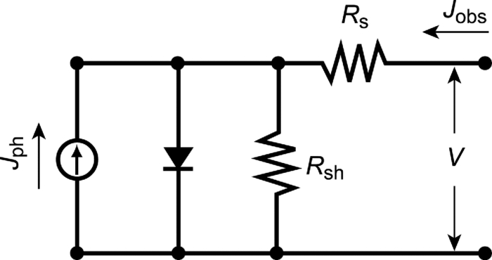
The dark current density is the sum of the current density that flows through the cell and the leakage current density that flows through the shunt resistance [Eq. 3] in the equivalent circuit of OPV devices (Fig. 4). Jobs is expressed as Eq. 4, where J0 is the reverse saturated dark current density, Rs and Rsh represents series and shunt resistances, respectively, V is the cell voltage, n is the diode ideal factor, k is the Boltzmann constant, and T is the absolute temperature. Numerical calculation for Eq. 4 clearly shows that Jobs at given cell voltages under VOC significantly decreases and hence, FF also significantly decreases as the series resistance Rs increases. The decrease in the Rs of the m-MTDATA and 2-TNATA layer caused by the p-doping with F4TCNQ is responsible for the enhancement of both Jobs and FF. There was no shunt resistance decrease by the doping (ca. 500 and 1200 Ωcm2 for device D and device E). Considering the low HOMO level of m-MTDATA and 2-TNATA (5.1, 5.15 eV)5, 49, 50 and the LUMO level of F4TCNQ (5.24 eV),44 electron transfer from the electron donor to the electron acceptor F4TCNQ is suggested to take place in the dark, resulting in the increase in the electrical conductivity of the F4TCNQ-doped m-MTDATA and TDATA [TeX:] \documentclass[12pt]{minimal}\begin{document}\begin{equation}
J_d = J_{diode} + J_{sh}
\end{equation}\end{document}
[TeX:] \documentclass[12pt]{minimal}\begin{document}\begin{equation}
J_{obs} = J_0 \left[ {\exp \left[ {\frac{{e(V - J_{obs} R_s)}}{{nkT}}} \right] - 1} \right] + \frac{{V - J_{obs} R_s }}{{R_{sh} }} - J_{ph}.
\end{equation}\end{document} VOC is the voltage where Jobs is zero. Although Eq. 4, which is applied for inorganic semiconductor photovoltaic devices, predicts that the VOC value is not affected by Rs, the decrease of VOC caused by the p-doping is due to the hole injection from the ITO electrode into the p-doped donor layer at a lower applied voltage because of the decreased resistance of the p-doped donor layer. The VOC value decreases as such injection dark current starts to flow at a lower cell voltage. Comparison of the J–V characteristics in the dark between device A and device D [Fig. 2] and between device B and device E [Fig. 2] clearly shows that the dark current density for device D and device E abruptly starts to increase at a lower cell voltage of ca. 0.2 V as compared with ca. 0.4 V for device A and device B. It is understood that charge-carrier injection from the electrode into the organic layer takes place for OPV devices and that hole injection from the anode into the p-doped donor layer is facilitated because of the increase in the electrical conductivity of the p-doped material. It was expected that the reduction of VOC can be compensated by incorporation of a thin layer of undoped m-MTDATA on the ITO electrode. From this viewpoint, the following device was fabricated: ITO/PEDOT:PSS (ca. 30 nm)/m-MTDATA (10 nm)/m-MTDATA: F4TCNQ (10:1.0) (40 nm)/C60 (50 nm)/LiF (0.1 nm)/Al (80 to 150 nm) (device F). Device F exhibited higher VOC than that for device D, maintaining almost the same JSC and FF as those obtained for device D, and hence, led to further enhancement of PCE (Fig. 5 and Table 1). 4.SummaryIn the present study, we have investigated how the p-type doping of electron donors with low solid-state ionization potentials, m-MTDATA and 2-TNATA, with a strong electron acceptor F4TCNQ, affects JSC, VOC, FF, and PCE of OPV devices, where C60 is used as an electron acceptor. The results demonstrated that the p-doping of the donor layer with F4TCNQ causes the increase in both JSC and FF accompanied by the decrease in VOC, leading to higher PCE. These characteristic features are explained in terms of the decreased bulk resistance of the donor layer caused by the p-doping. The reduction of VOC caused by the p-doping was partly compensated by the incorporation of a thin layer of undoped m-MTDATA on the ITO electrode, and hence, PCE was further enhanced. The present study shows that charge-transfer doping of organic materials to reduce their bulk resistance is an effective approach for improving the PCE of OPV devices. ReferencesC. W. Tang,
“Two-layer organic photovoltaic cell,”
Appl. Phys. Lett., 48 183
–185
(1986). http://dx.doi.org/10.1063/1.96937 Google Scholar
P. Peumans, A. Yakimov, and S. R. Forrest,
“Small molecular weight organic thin-film photodetectors and solar cells,”
J. Appl. Phys., 93 3693
–3723
(2003). http://dx.doi.org/10.1063/1.1534621 Google Scholar
S. R. Forrest,
“The path to ubiquitous and low-cost organic electronic appliances on plastic,”
Nature (London), 428 911
–918
(2004). http://dx.doi.org/10.1038/nature02498 Google Scholar
S. Günes, H. Neugebauer, and N. S. Sariciftci,
“Conjugated polymer-based organic solar cells,”
Chem. Rev., 107 1324
–1338
(2007). http://dx.doi.org/10.1021/cr050149z Google Scholar
Y. Shirota and H. Kageyama,
“Charge carrier transporting molecular materials and their applications in devices,”
Chem. Rev., 107 953
–1010
(2007). http://dx.doi.org/10.1021/cr050143+ Google Scholar
G. Yu, J. Gao, J. C. Hummelen, F. Wudl, and A. J. Heeger,
“Polymer photovoltaic cells: enhanced efficiencies via a network of internal donor-acceptor heterojunctions,”
Science, 270 1789
–1791
(1995). http://dx.doi.org/10.1126/science.270.5243.1789 Google Scholar
M. Hiramoto, H. Fujiwara, and M. Yokoyama,
“Three-layered organic solar cell with a photoactive interlayer of codeposited pigments,”
Appl. Phys. Lett., 58 1062
–1064
(1991). http://dx.doi.org/10.1063/1.104423 Google Scholar
J. J. M. Halls, C. A. Walsh, N. C. Greenham, E. A. Marseglla, R. H. Friend, S. C. Moratti, and A. B. Holmes,
“Efficient photodiodes from interpenetrating polymer networks,”
Nature (London), 376 498
–500
(1995). http://dx.doi.org/10.1038/376498a0 Google Scholar
P. Peumans, V. Bulović, and S. R. Forrest,
“Efficient photon harvesting at high optical intensities in ultrathin organic double-heterostructure photovoltaic diodes,”
Appl. Phys. Lett., 76 2650
–2652
(2000). http://dx.doi.org/10.1063/1.126433 Google Scholar
P. Peumans and S. R. Forrest,
“Very-high-efficiency double-heterostructure copper phthalocyanine / C60 photovoltaic cells,”
Appl. Phys. Lett., 79 126
–128
(2001). http://dx.doi.org/10.1063/1.1384001 Google Scholar
A. Yakimov and S. R. Forrest,
“High photovoltage multiple-heterojunction organic solar cells incorporating interfacial metallic nanoclusters,”
Appl. Phys. Lett., 80 1667
–1669
(2002). http://dx.doi.org/10.1063/1.1457531 Google Scholar
D. Gebeyehu, B. Maennig, J. Drechsel, K. Leo, and M. Pfeiffer,
“Bulk-heterojunction photovoltaic devices based on donor-acceptor organic small molecule blends,”
Sol. Energy Mater. Sol. Cells, 79 81
–92
(2003). http://dx.doi.org/10.1016/S0927-0248(02)00369-0 Google Scholar
J. Xue, S. Uchida, B. P. Rand, and S. R. Forrest,
“Asymmetric tandem organic photovoltaic cells with hybrid planar-mixed molecular heterojunctions,”
Appl. Phys. Lett., 85 5757
–5759
(2004). http://dx.doi.org/10.1063/1.1829776 Google Scholar
J. Xue, B. P. Rand, S. Uchida, and S. R. Forrest,
“A hybrid planar-mixed molecular heterojunction photovoltaic cell,”
Adv. Mater., 17 66
–71
(2005). http://dx.doi.org/10.1002/adma.200400617 Google Scholar
J. Y. Kim, S. H. Kim, H.-H. Lee, K. Lee, W. Ma, X. Gong, and A. J. Heeger,
“New architecture for high-efficiency polymer photovoltaic cells using solution-based titanium oxide as an optical spacer,”
Adv. Mater., 18 572
–576
(2006). http://dx.doi.org/10.1002/adma.200501825 Google Scholar
M. Y. Chan, S. L. Lai, K. M. Lau, C. S. Lee, and S. T. Lee,
“Application of metal-doped organic layer both as exciton blocker and optical spacer for organic photovoltaic devices,”
Appl. Phys. Lett., 89 163515
(2006). http://dx.doi.org/10.1063/1.2362974 Google Scholar
J. Y. Kim, K. Lee, N. E. Coates, D. Moses, T.-Q. Nguyen, M. Dante, and A. J. Heeger,
“Efficient tandem polymer solar cells fabricated by all-solution processing,”
Science, 317 222
–225
(2007). http://dx.doi.org/10.1126/science.1141711 Google Scholar
H.-Y. Chen, J. Hou, S. Zhang, Y. Liang, G. Yang, Y. Yang, L. Yu, Y. Wu, and G. Li,
“Polymer solar cells with enhanced open-circuit voltage and efficiency,”
Nature (London) Photon., 3 649
–653
(2009). http://dx.doi.org/10.1038/nphoton.2009.192 Google Scholar
G. P. Kushto, W. Kim, and Z. H. Kafafi,
“Flexible organic photovoltaics using conducting polymer electrodes,”
Appl. Phys. Lett., 86 093502
(2005). http://dx.doi.org/10.1063/1.1867568 Google Scholar
M. Kinoshita, N. Fujii, T. Tsuzuki, and Y. Shirota,
“Creation of novel light sensitive amorphous molecular materials and their photovoltaic properties,”
Synth. Met., 121 1571
–1572
(2001). http://dx.doi.org/10.1016/S0379-6779(00)01292-3 Google Scholar
Z. R. Hong, C. S. Lee, S. T. Lee, W. L. Li, and Y. Shirota,
“Bifunctional photovoltaic and electroluminescent devices using a starburst amine as an electron donor and hole-transporting material,”
Appl. Phys. Lett., 81 2878
–2880
(2002). http://dx.doi.org/10.1063/1.1509092 Google Scholar
T. Osasa, S. Yamamoto, and M. Matsumura,
“Organic solar cells by annealing stacked amorphous and microcrystalline layers,”
Adv. Funct. Mater., 17 2937
–2942
(2007). http://dx.doi.org/10.1002/adfm.200601172 Google Scholar
A. Cravino, P. Leriche, O. Alévêque, S. Roquet, and J. Roncali,
“Light-emitting organic solar cells based on a 3D conjugated system with internal charge transfer,”
Adv. Mater., 18 3033
–3037
(2006). http://dx.doi.org/10.1002/adma.200601230 Google Scholar
C. He, Q. He, Y. Yi, G. Wu, F. Bai, Z. Shuai, and Y. Li,
“Improving the efficiency of solution processable organic photovoltaic devices by a star-shaped molecular geometry,”
J. Mater. Chem., 18 4085
–4090
(2008). http://dx.doi.org/10.1039/b807456a Google Scholar
J. Lu, P. F. Xia, P. K. Lo, Y. Tao, and M. S. Wong,
“Synthesis and properties of multi-triarylamine-substituted carbazole-based dendrimers with an oligothiophene core for potential applications in organic solar cells and light-emitting diodes,”
Chem. Mater., 18 6194
–6203
(2006). http://dx.doi.org/10.1021/cm062111o Google Scholar
A. Cravino, S. Roquet, O. Alévêque, P. Leriche, P. Frère, and J. Roncali,
“Triphenylamine-oligothiophene conjugated systems as organic semiconductors for opto-electronics,”
Chem. Mater., 18 2584
–2590
(2006). http://dx.doi.org/10.1021/cm060257h Google Scholar
H. Kageyama, H. Ohishi, M. Tanaka, Y. Ohmori, and Y. Shirota,
“High performance organic photovoltaic devices using amorphous molecular materials with high charge-carrier drift mobilities,”
Appl. Phys. Lett., 94 063304
(2009). http://dx.doi.org/10.1063/1.3079399 Google Scholar
H. Kageyama, H. Ohishi, M. Tanaka, Y. Ohmori, and Y. Shirota,
“High-performance organic photovoltaic devices using a new amorphous molecular material with high hole drift mobility, tris[4-(5-phenylthiophen-2-yl)]amine,”
Adv. Funct. Mater., 19 3948
–3955
(2009). http://dx.doi.org/10.1002/adfm.200901259 Google Scholar
J. Zhang, Y. Yang, C. He, Y. He, G. Zhao, and Y. Li,
“Solution-processable star-shaped photovoltaic organic molecule with triphenylamine core and benzothiadiazole−thiophene arms,”
Macromolecules, 42 7619
–7622
(2009). http://dx.doi.org/10.1021/ma901896n Google Scholar
L. Xue, J. He, X. Gu, Z. Yang, B. Xu, and W. Tian,
“Efficient bulk-heterojunction solar cells based on a symmetrical D-π-A-π-D organic dye molecule,”
J. Phys. Chem. C, 113 12911
(2009). http://dx.doi.org/10.1021/jp902976w Google Scholar
H. Shang, H. Fan, Q. Shi, S. Li, Y. Li, and X. Zhan,
“Solution processable D-A-D molecules based on triphenylamine for efficient organic solar cells,”
Sol. Energy Mater. Sol. Cells, 94 457
–464
(2010). http://dx.doi.org/10.1016/j.solmat.2009.11.005 Google Scholar
J. Kwon, M. K. Kim, J.-P. Hong, W. Lee, S. Noh, C. Lee, S. Lee, and J.-I. Hong,
“4,4′,4″-Tris(4-naphthalen-1-yl-phenyl)amine as a multifunctional material for organic light-emitting diodes, organic solar cells, and organic thin-film transistors,”
Org. Electron., 11 1288
–1295
(2010). http://dx.doi.org/10.1016/j.orgel.2010.04.005 Google Scholar
H. Kageyama, H. Ohishi, M. Tanaka, Y. Ohmori, and Y. Shirota,
“Organic photovoltaic devices using an amorphous molecular material with high hole drift mobility, tris[4-(2-thienyl)phenyl]amine,”
IEEE J. Sel. Top. Quantum Electron., 16 1528
–1536
(2010). http://dx.doi.org/10.1109/JSTQE.2009.2039699 Google Scholar
H. Shirakawa, E. J. Louis, A. G. MacDiarmid, C. K. Chiang, and A. J. Heeger,
“Synthesis of electrically conducting organic polymers: hologen derivatives of polyacetylene, (CH)x,”
J. Chem. Soc. Chem. Commun., 578
–580
(1977). http://dx.doi.org/10.1039/c39770000578 Google Scholar
Handbook of Conducting Polymers, Marcel Dekker, New York
(1989). Google Scholar
Y. Shirota, N. Noma, Y. Shimizu, H. Kanega, I.-R. Jeon, K. Nawa, T. Kakuta, H. Yasui, and K. Namba,
“Preparation of electrically conducting polymers containing pendant π-electron systems by electrochemical doping, and properties and applications of doped polymers,”
Synth. Met., 41–43 3031
–3036
(1991). http://dx.doi.org/10.1016/0379-6779(91)91232-Y Google Scholar
Y. Shirota, T. Kakuta, H. Kanega, and H. Mikawa,
“Rectification and photovoltaic properties of a Schottky barrier cell using electrochemically-doped poly(N-vinylcarbazole),”
J. Chem. Soc. Chem. Commun., 1201
–1202
(1985). http://dx.doi.org/10.1039/c39850001201 Google Scholar
Y. Shirota, N. Noma, and H. Mikawa,
“Electrochemical doping of poly[4-(N,N-diphenylamino)phenylmethyl methacrylate], and rectification and photovoltaic properties,”
Synth. Met., 18 399
–404
(1987). http://dx.doi.org/10.1016/0379-6779(87)90912-X Google Scholar
A. Yamamori, C. Adachi, T. Koyama, and Y. Taniguchi,
“Doped organic light emitting diodes having a 650-nm-thick hole transport layer,”
Appl. Phys. Lett., 72 2147
–2149
(1998). http://dx.doi.org/10.1063/1.121304 Google Scholar
A. Higuchi, H. Inada, T. Kobata, and Y. Shirota,
“Amorphous molecular materials: Synthesis and properties of a novel starburst molecule, 4,4′,4″-tri(N-phenothiazinyl)triphenylamine,”
Adv. Mater., 3 549
–550
(1991). http://dx.doi.org/10.1002/adma.19910031105 Google Scholar
W. Gao and A. Kahn,
“Controlled p-doping of zinc phthalocyanine by coevaporation with tetrafluorotetracyanoquinodimethane: A direct and inverse photoemission study,”
Appl. Phys. Lett., 79 4040
–4042
(2001). http://dx.doi.org/10.1063/1.1424067 Google Scholar
X. Zhou, J. Blochwitz, M. Pfeiffer, A. Nollau, T. Fritz, and K. Leo,
“Enhanced hole injection into amorphous hole-transport layers of organic light-emitting diodes using controlled p-type doping,”
Adv. Funct. Mater., 11 310
–314
(2001). http://dx.doi.org/10.1002/1616-3028(200108)11:4<310::AID-ADFM310>3.0.CO;2-D Google Scholar
X. Zhou, M. Pfeiffer, J. Blochwitz, A. Werner, A. Nollau, T. Fritz, and K. Leo,
“Very-low-operating-voltage organic light-emitting diodes using a p-doped amorphous hole injection layer,”
Appl. Phys. Lett., 78 410
–412
(2001). http://dx.doi.org/10.1063/1.1343849 Google Scholar
J. Endo, T. Matsumoto, and J. Kido,
“Organic electroluminescent devices with a vacuum-deposited Lewis-acid-doped hole-injecting layer,”
Jpn. J. Appl. Phys., 41 L358
–L360
(2002). http://dx.doi.org/10.1143/JJAP.41.L358 Google Scholar
M. Ishihara, K. Okumoto, T. Tsuzuki, H. Kageyama, H. Nakano, and Y. Shirota,
“Electrically conducting amorphous molecular material: Iodine doped m-MTDATA as a hole injection buffer layer in organic electroluminescent devices,”
Mol. Cryst. Liq. Cryst., 455 259
–266
(2006). http://dx.doi.org/10.1080/15421400600698667 Google Scholar
Y. Shirota, Y. Kuwabara, H. Inada, T. Wakimoto, H. Nakada, Y. Yonemoto, S. Kawami, and K. Imai,
“Multilayered organic electroluminescent device using a novel starburst molecule, 4,4′,4″-tris(3-methylphenylphenylamino)triphenylamine, as a hole transport material,”
Appl. Phys. Lett., 65 807
–809
(1994). http://dx.doi.org/10.1063/1.112238 Google Scholar
Y. Shirota, Y. Kuwabara, D. Okuda, R. Okuda, H. Ogawa, H. Inada, T. Wakimoto, H. Nakada, Y. Yonemoto, S. Kawami, and K. Imai,
“Starburst molecules based on π-electron systems as materials for organic electroluminescent devices,”
J. Lumin., 72–74 985
–991
(1997). http://dx.doi.org/10.1016/S0022-2313(96)00396-1 Google Scholar
Y. Shirota,
“Organic materials for electronic and optoelectronic devices,”
J. Mater. Chem., 10 1
–25
(2000). http://dx.doi.org/10.1039/a908130e Google Scholar
Y. Shirota,
“Photo- and electroactive amorphous molecular materials – molecular design, synthesis, reactions, properties, and applications,”
J. Mater. Chem., 15 75
–93
(2005). http://dx.doi.org/10.1039/b413819h Google Scholar
Y. Shirota, T. Kobata, and N. Noma,
“Starburst molecules for amorphous molecular materials. 4,4′,4″-Tris(N,N-diphenylamino)triphenylamine and 4,4′,4″-tris[N-(3-methylphenyl)-N-phenylamino]triphenylamine,”
Chem. Lett., 1145
–1148
(1989). http://dx.doi.org/10.1246/cl.1989.1145 Google Scholar
C. Giebeler, H. Antoniadis, D. D. C. Bradley, and Y. Shirota,
“Space-charge-limited charge injection from indium tin oxide into a starburst amine and its implications for organic light-emitting diodes,”
Appl. Phys. Lett., 72 2448
–2450
(1998). http://dx.doi.org/10.1063/1.121392 Google Scholar
Y. Shirota, K. Okumoto, H. Ohishi, M. Tanaka, M. Nakao, K. Wayaku, S. Nomura, and H. Kageyama,
“Charge transport in amorphous molecular materials,”
Proc. SPIE-Int. Soc. Opt. Eng., 5937 593717
(2005). http://dx.doi.org/10.1117/12.620255 Google Scholar
S. C. Tse, K. C. Kwok, and S. K. So,
“Electron transport in naphthylamine-based organic compounds,”
Appl. Phys. Lett., 89 262102
(2006). http://dx.doi.org/10.1063/1.2420785 Google Scholar
S. C. Tse, S. W. Tsang, and S. K. So,
“Polymeric conducting anode for small organic transporting molecules in dark injection experiments,”
J. Appl. Phys., 100 063708
(2006). http://dx.doi.org/10.1063/1.2348640 Google Scholar
R. A. Marsh, C. Groves, and N. C. Greenham,
“A microscopic model for the behavior of nanostructured organic photovoltaic devices,”
J. Appl. Phys., 101 083509
(2007). http://dx.doi.org/10.1063/1.2718865 Google Scholar
J. Y. Lee and J. H. Kwon,
“Enhanced hole transport in C60-doped hole transport layer,”
Appl. Phys. Lett., 88 183502
(2006). http://dx.doi.org/10.1063/1.2172296 Google Scholar
B. Maennig, M. Pfeiffer, A. Nollau, X. Zhou, K. Leo, and P. Simon,
“Controlled p-type doping of polycrystalline and amorphous organic layers: Self-consistent description of conductivity and field-effect mobility by a microscopic percolation model,”
Phys. Rev. B, 64 195208
(2001). http://dx.doi.org/10.1103/PhysRevB.64.195208 Google Scholar
BiographyTakao Umeda has been working for Fukui University of Technology. His research activities are concerned with the fabrication and performance analysis of optoelectronic devices such as organic electroluminescent devices, organic photovoltaic devices, and dye-sensitized solar cells. Keigo Chujo, Yasuhiro Nomura, and Kotaro Tsuchida are students of Graduate School of Engineering, Fukui University of Technology. Michihiro Hara received is DE degree from Osaka University in 2003. He worked for the Institute of Science and Technology, Osaka University from 2003 to 2005. He moved to Fukui University of Technology as an assistant professor in 2005 and promoted to associate professor in 2008. His research fields cover laser photochemistry and the fabrication and performance analysis of organic light-emitting diodes and organic solar cells. Sayo Terashima graduated from Osaka University, Department of Applied Chemistry, Faculty of Engineering and received her BE degree. She has been working for The Kansai Electric Power Co. Yasuhiro Koji finished the Master course of Graduate School of Engineering Science, Osaka University and received his ME degree. He has been working for The Kansai Electric Power Co. Hiroshi Kageyama obtained his BE (1992) from Department of Applied Chemistry, Faculty of Engineering, Osaka University, and his ME (1994) and PhD degrees (1997) from Graduate School of Engineering, Osaka University. He was appointed to be research associate at Osaka University in 1997 and has been assistant professor since 2006. His research area covers charge transport in organic disordered systems and organic electronics. Yasuhiko Shirota received his DE degree from Osaka University in 1968. He was appointed to be research associate at Osaka University in 1968, promoted to associate professor in 1972, and full professor in 1986. Since 2003, he has been professor Emeritus of Osaka University and professor at Fukui University of Technology. His research interest covers a wide field of organic materials science including synthesis, structures, reactions, properties, functions of both molecular materials and polymers, and their applications in devices. |