|
|
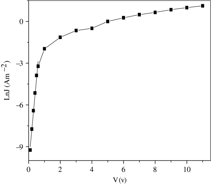
1.IntroductionConducting polymers have been the subject of considerable recent interest because of their unique electrical and optical properties. Conjugated polymers have been widely used as a promising candidate for low-cost organic/molecular electronic applications. Polyaniline (PANI), one of the most technologically important classes of conjugated polymers, owes its popularity to its high conductivity in the doped state and its excellent thermal and electrochemical stability.1, 2 Schottky devices based on conjugated polymers are particularly attractive because of their ease and cheapness of fabrication, high electrical conductivity, and good environmental stability under ambient conditions. Another advantage of the polymers is that it does not need surfaces with regularity at the atomic level in contrast to inorganic semiconductors.3 In this paper, we present the preparation and characterization of Schottky barriers based on PANI–poly (methylmethacrylate) (PMMA) blend. Various junction parameters have been calculated using current density–voltage (J–V) in the dark and under illumination, and capacitance–voltage (C–V) characteristics. The ac impedance of the blend is measured and the results are discussed. 2.ExperimentalPANI–PMMA blend films were made as follows: polyaniline (emeraldine) base powder was dissolved in dimethylformamide (DMF) to prepare a stock solution with concentration of 1 wt %, and filtering of the solution to remove undissolved particles. PMMA powder was dissolved in DMF and mixed with stock solution of polyaniline. The concentration of PANI in PMMA was maintained at 10% by weight. The solution was used for preparation of films by drop-casting onto glass plates. The peeled film was cut into pieces suitable for measurements and then placed in a vacuum chamber maintained at 10−4 Torr to remove the water vapour and other volatile additives used in the original preparation of the film. The films were removed to a desiccator and stored in dry air for several days before the electrodes were deposited to complete the structure. The thickness of the films so obtained was approximately 1 mm. Finally, Au foil of thickness 20 μm was used to produce a so-called Schottky barrier4 with the freshly prepared blend, while 10 μm thick Al foil acted as the ohmic contact. Foil electrodes are used because vacuum evaporation of aluminum on PANI often resulted in noise in J–V characteristics.1 In general, metal possessing a low work function, such as Al (φAl = 3.7 eV), gives ohmic contacts, while metal possessing a high work function,4 such as Au (φAu = 5.1 eV), provides rectifying contacts that indicated n-type behavior for the PANI–PMMA blend in the device. The sample was sandwiched between the two electrodes and mounted in the sample holder consisting of two parallel circular condenser made of copper of 1.2 ×10⁻²–m diameter. The sample holder was then mounted inside a closed chamber that was evacuated using a simple roughing pump. The electrical contacts for electrical leads were made by conducting silver paint. The completed devices had an active area of ≈ 0.5×10⁻⁴ m2. Electrical measurements were performed at room temperature 295 K using a Keithley 614 electrometer and a stabilized power supply. Forward bias is defined as the aluminum electrode being negatively biased. The photo-measurements were measured using 7 Wm−2 monochromatic radiation of a He–Ne laser diode (model HLM 1230). C–V and complex impedance measurements were carried out with a HIOKI (3532) LCR meter. 3.Results and DiscussionThe forward and reverse J–V characteristics are shown in Fig. 1 for a typical Au/PANI–PMMA/Al device at room temperature. It is clear from Fig. 1 that the forward current increases exponentially at a lower voltage region and linearly at a higher voltage region. An asymmetric and nonlinear J–V curve shows that the device exhibits rectification behavior. The room temperature conductivity of the blend is estimated from the slope of the J–V characteristics in the ohmic region and is found to be 3×10⁻³ Sm−1. Fig. 1Current density (J) versus voltage (V) characteristics for the device. Inset shows the variation of J versus of V at low voltage V<1.  The mode of carrier transport of charge from the PANI–PMMA blend to metal (Au) over the potential barrier is now analyzed with the J–V relation of a Schottky diode as follows:5 [TeX:] \documentclass[12pt]{minimal}\begin{document}\begin{equation}
J_f = J_0 (\exp ^{eV/nkT} - 1),
\end{equation}\end{document} where J0 is the saturation current density, e is the electron charge, V is the applied voltage, n is the ideality factor, k is Boltzmann's constant, and T is the absolute temperature. J0 can be related to the effective barrier height at zero bias φb by
[TeX:] \documentclass[12pt]{minimal}\begin{document}\begin{equation}
J_0 = A^ * T^2 \exp ^{ - e\varphi _b /kT},
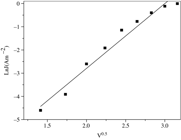
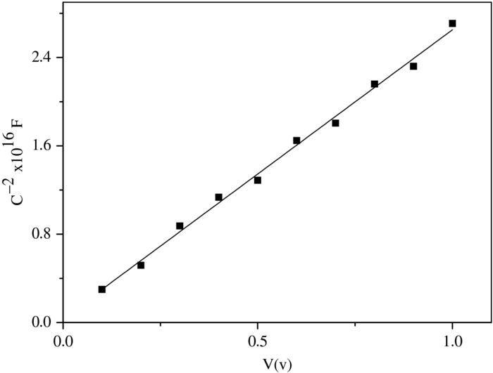
\end{equation}\end{document} where A* is the effective Richardson constant.One can determine φb by making a ln J versus V plot under forward bias. Figure 2 shows the ln J versus V plot of Au/ PANI–PMMA barrier in the forward bias condition. It can be seen from Fig. 2 that the curve deviates from a straight line fit above 0.6 V. Above this threshold voltage the Schottky barrier disappears and the current could be limited primarily by the bulk resistance of the blend or space charge limited region.6 The slope of the linear part of the curve gives the value of n. The calculated value of n is 3.2. This value is comparable to that of the PANI–PMMA blend/metal Schottky barrier.4 However, the ideality factor is so high that it is not more in accordance with the thermionic mode of current transport. Probably another mechanism controls the current flow. This mechanism might be electron tunneling between the particles. Besides this, various other phenomena like barrier height inhomogeneity, recombination—generation,3 bulk resistance, and Poole–Frenkle effects may be responsible for the observed high values of ideality factors. The extrapolated value of current density J at zero voltage (Fig. 2) is the saturation current J0. Assuming φb = 0.39 eV as derived from the C–V measurements, the value of A* is 1.9×10⁻³ A m−2 K−2. The value of A* is very low in comparison to A* for free electron 1.20 ×10⁶ A m−2 K2 informing that the diffusion mechanism is more dominant.1, 2 Similar lower values for A* have been reported for Al\sulfate –doped polyaniline, Al\methane sulfonate–doped polyaniline junctons,1 and metal/Cl3-doped poly(paraphenyl) Schottky barriers.7 The voltage dependence of the reverse current can be written as,5 [TeX:] \documentclass[12pt]{minimal}\begin{document}\begin{equation}
J = A^* T^2 \exp ^{ - \varphi_ b/KT} \exp ^{\beta V^{1/2} /KT},
\end{equation}\end{document} where β is the field lowering coefficient related to the barrier width.The linear behavior in the plot of the current density ln J versus V1/2 as shown in Fig. 3 indicates that the J–V characteristic is consistent with Eq. 3. The estimated value of β is 0.071 eV·V−1/2. The Schottky barrier can be further characterized using a C–V measurement. It has been observed that the junction has a specific capacitance due to a space charge in the depletion layer. It is related to the width of the depletion region and therefore depends on junction voltage. The plot of C−2 versus reverse bias voltage displayed in Fig. 4 is linear which indicates the formation of a Schottky junction.8 Therefore, it follows a standard Mott–Schottky relationship9 [TeX:] \documentclass[12pt]{minimal}\begin{document}\begin{equation}
\frac{1}{{C^2 }} = \frac{{2(V_d - V - kT/e)}}{{e\varepsilon \varepsilon _0 NA^2 }},
\end{equation}\end{document} where Vd is the built –in potential, N is the charge carrier concentration, A is the effective area of the device, ɛ0 is the permittivity of the free space, ɛ is the relative permittivity of polymer blend, and the other symbols have their usual meanings. In addition, the permittivity of the PANI-PMMA film has been evaluated from capacitance measurements using the equation C = ɛɛ0A/d, where C is the measured capacitance and d is the thickness of the film. The value of ɛ is found to be ∼3.From the slope of the straight line shown in Fig. 5, charge carrier concentration N is ≅ 7.2 × 10²¹ m−3. This value of N correlates well with previously published data.2 It is evident from Eq. 4 that the intercept on the abscissa gives the built-in potential Vd = 0.06 eV rather than the barrier height φb. The two quantities are related by the following equation:10 [TeX:] \documentclass[12pt]{minimal}\begin{document}\begin{equation}
\varphi _b = V_d + \frac{{KT}}{e}\left(1 + \ln \frac{{N_v }}{N}\right).
\end{equation}\end{document}
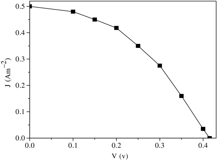
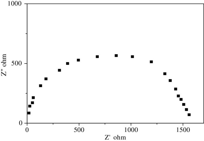
Substituting the values of N, Vd, and NV (assumed to have the value of 1027 m−3) in Eq. 5, the derived value of φb is 0.39 eV. The capacitance of the device at zero C0 bias is ≅ 31.3 nF, which corresponds to a thickness of depletion region (ω = ɛɛ0 A /C0) of 4.2 × 10⁻⁴ m. A typical J–V curve obtained under constant illumination of 7 Wm−2 is shown in Fig. 5. The photovoltaic cell values such as open-circuit voltage Voc, short-circuit current Jsc, the fill factor ff and the power conversion efficiency η are found to be, respectively, Voc = 0.415 V, Jsc = 0.510 A m−2, ff = 0.413, and η = 1.25%. Further information about the bulk resistance and Schottky junction parameters were obtained from impedance measurements. In the present study, Ag and Al foils were used to make contacts with PANI-PMMA blend in contrast to vacuum-evaporated electrodes. During vacuum evaporation, an insulated layer has been reported to be formed between metal electrode and the blend, which ultimately resulted in a high-frequency bias voltage-independent semicircle overlapped with the bias voltage-independent low-frequency semicircle for the depleting layer.1 The Cole–Cole plot of the complex impedance Z = Z′ +i Z″ [Real (Z) versus Im (Z)] in the frequency range of 60 Hz to 5 MHz at room temperature is shown in Fig. 6. The figure reveals that the impedance response is a single semicircle. This indicates the absence of contact effects and the relaxation is obeyed by the Debye model. The classical semicircular form can be represented by a simple parallel Rd-Cd circuit, where Rd and Cd represents the resistance and capacitance of the depletion layer.11 The values of Cd and Rd are given by: [TeX:] \documentclass[12pt]{minimal}\begin{document}\begin{equation}
\begin{array}{lr}
C_d = \mathop {\lim }\limits_{\upsilon \to \infty } [ - \omega Z''(f)]^{ - 1} &\\[-5pt]
&,\\[-5pt]
R_d = \mathop {\lim }\limits_{\upsilon \to 0} Z'(f)& \\
\end{array}
\end{equation}\end{document} where ω = 2πf is the angular frequency and f is the frequency.The room temperature conductivity estimated from the intercept on the real axis of Fig. 6 is found to be around 1.25 ×10⁻² Sm−1 which is slightly higher than the value ≈ 3×10⁻³ Sm−1 evaluated from the slope of the J–V characteristics. It has been reported that in the case of PMMA-PANI composite fibers, the values of the dc conductivities evaluated from the J–V characteristics and the complex impedances are different by a factor of ∼6.12 Therefore, the difference in the conductivity values may be attributed to the different methods used to analyze the experimental results. The value of the conductivity is about 4 orders less compared to that of the pure PANI sample. This is accepted since blending PANI with an insulating polymer would reduce the conductivity. Nevertheless, if we compare with the conductivity of pure PMMA ∼10−13 Sm−1 there is nearly 11 orders of magnitude.12 The relaxation time, τ has been determine from 1/ωmax, where ωmax corresponds to the maximum of the imaginary part of the impedance. A value of τ ≈ 1.6 μs thus obtained agrees with the values listed in the literature.13 4.ConclusionIn our study, we have fabricated a polyaniline-poly (methyl methacrylate) blend/Ag Schottky structure. The electronic parameters such as ideality factors, barrier height, built-in potential at zero bias, depletion width, and space-charge-density were extracted from J–V and C–V measurements. The photovoltaic parameters of the cells have been determined from the current–voltage characteristics under a constant illumination of 7 mW. The almost semicircle behavior of the Cole–Cole plot (Z″-Z′) indicates the absence of contact effects and the relaxation is obeyed by the Debye model. ReferencesS. F. Chung, T. C. Wen, and A. Gopalan,
“Influence of dopant size on the junction properties of polyaniline,”
Mater. Sci. Eng. B, 116 125
–130
(2005). http://dx.doi.org/10.1016/j.mseb.2004.09.023 Google Scholar
H. A. Motaweh and T. G. Abdel-Malik,
“Schottky barrier formation using composite of polyaniline containing iron oxides,”
(2008). Google Scholar
S. Sönmezoğlu, S. Şenkul, R. Taş, G. Çankaya, and M. Can,
“Electrical and interface state density properties of polyaniline–poly-3-methyl thiophene blend/p-Si Schottky barrier diode,”
Solid State Sciences, 12
(5), 706
–711
(2010). http://dx.doi.org/10.1016/j.solidstatesciences.2010.02.001 Google Scholar
S. Angappane, K. N. Rajeev, T. S. Natarajan, G. Rangarajan, and B. Wessling,
“PAni–PMMA blend/metal Schottky barriers,”
Thin Solid Films, 417 202
–205
(2002). http://dx.doi.org/10.1016/S0040-6090(02)00576-X Google Scholar
S. M. Sze, Physics of Semiconductor Devices, John Wiley, New York
(1993). Google Scholar
S. S. Pandey, M. K. Ram, V. K. Srivastava, and B. D. Malhotra,
“Electrical properties of metal (indium)/polyaniline Schottky devices,”
J. Appl. Polym. Sci., 65
(13), 2745
–2748
(1998). http://dx.doi.org/10.1002/(SICI)1097-4628(19970926)65:13<2745::AID-APP17>3.0.CO;2-W Google Scholar
M. Camps and B. Bellow,
“Properties of metal-poly(p-phenylene) Schottky barriers,”
J. Phys. D: Appl. Phys., 26 1274
–1277
(1993). http://dx.doi.org/10.1088/0022-3727/26/8/018 Google Scholar
C. Coskun, S. Aydogan, and H. Efeoglu,
“Temperature dependence of reverse bias capacitance–voltage characteristics of Sn/p-GaTe Schottky diodes,”
Semicond. Sci. Technol., 19
(2), 242
–246
(2004). http://dx.doi.org/10.1088/0268-1242/19/2/020 Google Scholar
E. H. Rhoderick and R. H. Williams, Metal Semiconductor Contacts, 2nd Ed.Oxford University Press, Oxford, UK
(1988). Google Scholar
T. G. Abdel-Malik,
“Temperature dependence studies of the low-frequency capacitance measurements in α and β-iron phthalocyanines,”
Thin Solid Films, 205
(2), 241
–245
(1991). http://dx.doi.org/10.1016/0040-6090(91)90308-K Google Scholar
T. G. Abdel-Malik, M. E. Kassem, N. S. Aly, and S. M. Khalil,
“AC conductivity of cobalt phthalocyanine,”
Acta Physics Polonica (A), 81 675
–680
(1992). Google Scholar
B. V. Jagadeesh, K. K. Satheesh, D. C. Trivedi, M. V. Ramakrishna, and N. T. Srinivasan,
“Electrical properties of electrospun fibers of PANI-PMMA composites,”
J. Engineered Fibers and Fabrics, 2 25
–31
(2007). Google Scholar
P. Dutta, S. Biswas, M. Ghosh, S. K. De, and S. Chatterjee,
“The dc and ac conductivity of polyaniline–polyvinyl alcohol blends,”
Synth. Met., 122 455
–461
(2001). http://dx.doi.org/10.1016/S0379-6779(00)00588-9 Google Scholar
|