|
|
1.IntroductionThe solar cell is a device that transfers light energy to electric power. Most devices use a semiconductor as the active material to absorb light. Silicon has demonstrated reliable performance and is cost effective, compared to the III–V semiconductor and ripe techniques for the industry. However, silicon has a large refractive index, reflecting about 36% of incident light power over the wavelength of interest in solar cell work. The huge optical loss heavily influences light harvesting. Therefore, light trapping is a very important technique for increasing solar cell efficiency. Two practical techniques solve the optical loss of surface reflection. The first technique is surface texturization that increases light absorption in silicon. Many publications1, 2 , 3 have investigated the effects of surface texturing structures. Most productions have used acid-texturization for the SiNx-based multicrystalline (mc-Si) solar cell and alkaline-texturization for the single crystalline silicon (sc-Si) solar cell. Some groups have modified or created a new textured structure, for example, the nanoporous structure4 or the honeycomb structure,5 but these often involve other side effects, such as poor electrical properties or increased process complexity. The second technique, surface antireflection layer coatings (ARC),6, 7 uses an antireflective coating technique based on thin-film optics. A multilayer ARC obtains better optical performance, improving wavelength range or reflection ratio, and can be fabricated after completing the cell process. Therefore, the coating process does not degrade cell performance. However, the ARC condition depends on the thickness and dielectric constant of the coated film, controlled by the ripe coating technique. Previous studies have reported different ARC combinations of dielectric materials for the solar cell,8, 9 , 10 widely applied in the solar cell field. Yi11 reported double layer ARC of MgF2/SiNx for mc-Si and sc-Si solar cells, adding a 75-nm MgF2 layer on the normal cell, but without further study and optimization. The current study investigates the simulation results of double layer ARC on the texturing surface and compares the experimental results to explore its trends. This work demonstrates the best MgF2 thickness for the mc-Si solar cell, improving the short circuit current and efficiency of small cells and product-oriented cells. 2.Theory and SimulationThis study chose the ARC layer thickness to be a quarter wavelength of the incident wave. The single ARC layer is typically used with amorphous hydrogenated silicon nitride (SiNx:H) for mc-Si solar cells, coated by plasma-enhanced chemical vapor deposition (PECVD). The refractive index of SiNx is about the range of 1.9 to 2.1 and the SiNx layer thickness is about 80 to 110 nm for the mc-Si solar cell. The minimum reflectance is near 500 to 600 nm to match the solar spectrum. The ARC has other functions, such as surface passivation and H-passivation for mc-Si solar cells,12 making it difficult to replace with other materials. This study did not choose other dielectric materials to replace the SiNx layer for the MgF2/SiNx double ARC design, to maintain its electrical performance of original mc-Si solar cells. The lower refractive index material of MgF2 was a top layer of double ARC. This research optimized its thickness condition to enlarge the absorption spectrum range of solar cells. According to the theory of film optics, the refractive index of the double layer follows Eq. 1 for the air environment condition:11 [TeX:] \documentclass[12pt]{minimal}\begin{document}\begin{equation}
n_1^3 = n_{{\rm si}},
\end{equation}\vspace*{-38pt}\end{document}
[TeX:] \documentclass[12pt]{minimal}\begin{document}\begin{equation}
n_2^3 = n_{{\rm si}}^2,\vspace*{-6pt}
\end{equation}\end{document}
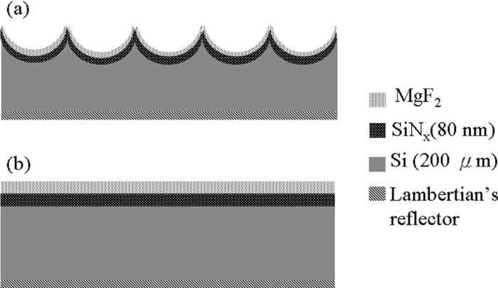
where nsi, n2, and n1 are the refractive index of the silicon substrate, the bottom and top layer of the attached silicon substrate are close to the air environment. The optimal thickness for each layer follows the quarter wavelength principle. According to Eqs. 1, 2 calculations, the refractive index n1 and n2 of the zero-reflection condition is relatively 1.58 and 2.5. However, they cannot be used on the ARC design for conventional mc-Si solar cells for two reasons: (1) using the SiNx layer on the mc-Si solar cell limits the materials of the bottom layer, due to the previous descriptions. (2) Surface texturization in the mc-Si solar cells decreases the interface reflection. Acid etches the textured structures to form concave micron-sized structures, such as the irregular bowl, followed by ARC film coating on these structures. The incident angle of solar light is not a fully normal incident on the textured structures. Predicting the quarter wavelength principle is inaccurate, and only serves as a reference; using the optical simulation tool solves complicated problems and improves prediction accuracy.This study used the commercial optical ray-tracing package software (ASAP) to design ARC conditions. Figure 1 shows the cross-section of simulated structures, using the silicon substrate with 200-μm thickness. This investigation compared two surface conditions, Fig. 1 shows the flat silicon surface, and Fig. 1 shows the textured silicon surface that is fully filled by 10-μm diameter semisphere bowl-shape structures and forming the honeycomb periodic array. This research designed these structures by coating 80-nm SiNx film on top of the silicon surface and chose MgF2 for the second layer on the SiNx film. Its refractive index used the optic handbook.13 The simulation thickness changed from 0 to 250 nm, adding 25 nm per condition. The backside of the silicon substrate exhibited a total reflective Lambertian's surface. The incident light source used an AM 1.5G solar spectrum. This work combined the absorption spectrum from simulation and the internal quantum efficiency of the measured silicon to calculate the photocurrent density of the solar cell. 3.ExperimentThe 15.6 × 15.6 cm2 p-type mc-Si substrates were processed to solar cells according to the standard industrial process flow, including removing saw damage, acid-texturing, emitter diffusion from POCl3, removing phosphate glass (PSG), and edge isolation, SiNx:H passivation and ARC layer coated from PECVD, screen printing front and back electrodes, and co-firing the metal contact. Figure 2 shows the scanning electron microscope (SEM) pictures of mc-Si solar cell and presented the irregular bowl-like textured structures. This study chose the low refractive index material MgF2 as a top layer of the double ARC layer and investigated the thickness effect of the top layer. The MgF2 layer was coated by an E-gun coater to ensure its coating uniformity with rotated samples in the deposition. An in-situ thickness monitor decided the coating thickness. Fig. 2SEM pictures of mc-Si solar cell: (a) the cell surface of top view and (b) the cell cross-section of side view. The white scale bars show the length (a) 2000 nm and (b) 100 nm.  Changing the MgF2 thickness makes it possible to change cell reflectivity and influence photoelectron conversion efficiency of solar cells. These samples measured the reflective spectrum to compare with the simulation results. The measurement of all reflectance spectrums used the integrating sphere and the measured samples were tilted 8 deg with incident light to collect total reflection. The solar simulator measured cell efficiency. To prevent measured error between before and after the MgF2 coating process, we chose some cells as reference cells and normalized the measured data of all cells by the reference cells. The experiment used the AM1.5G solar simulator to measure 4 × 4 cm2 size cells to obtain the trends of short circuit current (Isc) and efficiency with different MgF2 thicknesses, and measured the 15.6 × 15.6 cm2 product class cells to prove the efficiency improvement of double layer ARC mc-Si solar cells. 4.Results and DiscussionThe SiNx film provides an ultra-low surface recombination velocity (SRV)12 on p-type silicon cells and can widely tune its refractive index from 1.8 to 2.6 by optimizing the NH3 and SiH4 flow ratio.6 The unique properties make SiNx film irreplaceable by other materials for the double ARC film. As mentioned in Sec. 2, the double layer design has lower reflection on the broadband range compared with the single ARC. When the refractive index of the top and bottom layer is relatively set at about 1.5 and 2.3 from Eqs. 1, 2, it forms a W-shaped reflectance spectrum with the two lowest reflection points. However, the SiNx film with a refractive index of 2.3 has higher absorption loss in the range of 300 to 500 nm.6 A more suitable refractive index needs to be smaller than 2 to avoid material absorption loss on the solar spectrum range (>400 nm). The refractive index of the top layer should be lower than 1.5 to match the solar spectrum. MgF2 has good mechanical properties and is a low refractive index material. We chose the material to be a top layer of double ARC film. Figure 3 shows the simulated results of cells with flat and textured surfaces. The transverse axis shows the incident light wavelength and the longitudinal axis shows the cell reflection. The black-square-symbol line and black-triangle-symbol line present the reflection of 80 nm SiNx for the single ARC with a flat and textured structure. The lowest point at about 650 nm for the reflection spectrum is a common property of the single ARC. The incident light illuminating on the textured surface more than doubles the reflection on the surface to increase the opportunities of light coupled into the silicon material, therefore the reflection is lower than the flat surface. According to the textured structure of Fig. 1, it is assumed the structures had not experienced more than double reflection and ignored the large angle incident light. This study used the simple trigonometric functions to calculate the ratio of area with single reflection and double reflection for the concave semisphere structure. The calculated results were that the occupied area of single reflection is one-third and the double reflection is two-thirds. Therefore, the simple estimation formula of reflection for the bowl-like textured surface is given by Eq. 3: [TeX:] \documentclass[12pt]{minimal}\begin{document}\begin{equation}
R_{{\rm textured}} (\lambda ) = \frac{{R_{{\rm flat}} (\lambda )}}{3} + \frac{{2R_{{\rm flat}}^2 (\lambda )}}{3},
\end{equation}\end{document}
where Rtextured is the reflection of the textured surface and Rflat is the reflection of the flat surface. The calculated results are similar to simulation results. This method can roughly evaluate new ARC structures before simulation. Figure 3 shows the reflection of the flat (black-circle-symbol line) and textured (black-star symbol line) surface with 125 nm MgF2 and 80 nm SiNx double ARC. They obviously form W-shaped reflection curves and two lowest points, with saddle-points at the 645-nm wavelength. The textured surface reflection is smaller than the flat surface and roughly follows the rule of Eq. 3, presenting a smaller than 5% reflection loss in the wavelength range of 450 to 1200 nm.Fig. 3Reflectance spectrum of simulation structures (Fig. 1) with 0 nm MgF2 and 125 nm MgF2 thickness. The black-square-symbol line is the single ARC with a flat surface, the black-triangle-symbol line is the single ARC with a textured surface, the black-circle-symbol line is the double ARC with a flat surface, and the black-star-symbol line is the double ARC with a textured surface.  To obtain photocurrent density trends with different double ARC conditions, we simulate the reflection spectrum to couple with the solar spectrum and silicon internal quantum efficiency (IQE). Equation 4 shows the photocurrent density formula (Jph) using simulated silicon absorption spectrum with different MgF2 thickness, the AM1.5G solar spectrum, and the measured IQE:6 [TeX:] \documentclass[12pt]{minimal}\begin{document}\begin{equation}
J_{{\rm ph}} = \int\limits_\lambda {\frac{{e\lambda }}{{hc}}(1 - R(\lambda ))I_{{\rm AM}1.5{\rm G}} (\lambda ){\rm IQE}(\lambda ){\rm d}\lambda },
\end{equation}\end{document}
where e is the electron charge, h is the Planck constant, c is the light velocity, λ is the light wavelength, R(λ) is the reflectivity, IAM 1.5G(λ) is the AM1.5G solar spectrum, and IQE(λ) is the measured internal quantum efficiency of mc-Si solar cells. Figure 4 shows the simulated results of photocurrent density for the cells flat and textured surfaces to compare different MgF2 thicknesses. We calculated one data point per 25-nm interval. The best MgF2 thickness with highest photocurrent density is located in the MgF2 thickness ranging from 100 to 125 nm. The textured case has lower photocurrent enhancement than the flat case due to double reflection on the textured surface, but the trends are similar to the flat surface. When MgF2 thickness is more than 150 nm, the photocurrent of the double ARC is smaller than the single ARC.Fig. 4The relation of photo-current density and MgF2 thickness for the double ARC cells. The black-square-dotted line is the flat surface. The black-triangle-dotted line is the textured surface.  Figure 5 shows the reflection spectrum of the simulated textured surface and the measured mc-Si solar cell for different MgF2 thicknesses. The lowest point wavelength of 50 nm MgF2 thickness shifts to 750 nm to compare the single ARC. The reflection spectrum of 250 nm MgF2 thickness presents the W-shaped reflection performance. The experimental data show about 2.5% reflection offset larger than the simulation, caused by the leakage of an integrating sphere. The practical acid-texturization surface structures14 are random and the irregular bowl-like shape exhibits-slight difference with the honeycomb structure of our simulation. However, the results of simulation and measurement are similar, except in the ultraviolet wavelength range, because we assumed that the extinction coefficient k of SiNx film was zero for the simulation. In fact, the SiNx film of real mc-Si solar cell was small k at the 400 nm wavelength.6 Fig. 5Reflectance spectra of 0 nm (black-circle line), 50 nm (white-square line), and 250 nm (black-triangle line) MgF2 thickness: (a) simulated and (b) measured spectra of the mc-Si solar cells.  Figure 6 shows the reflection spectrum of an mc-Si solar cell with 75-nm MgF2 thickness and without MgF2 coating. The reflectance of 75-nm MgF2 thickness case is lower than without MgF2 coating case in the all-wavelength range except ranging from 500 to 700 nm. Figure 6 shows the external quantum efficiency (EQE) ratio which is the EQE of 75 nm MgF2 thickness case divided by without the MgF2 coating case. The curve of the EQE ratio shows enhancement on the 400 to 500 nm and 700 to 1000 nm wavelength range. The trend of the EQE ratio is coincident with reflectance spectrum of Fig. 6. This proved the lower reflectance can harvest the light into the cell and increase the photo-current density of the mc-Si solar cell. Fig. 6(a) Reflectance spectra of 0 nm (black-triangle line), 75 nm (white-square line) MgF2 thickness, (b) EQE ratio spectra. The dashed-line is no enhancement.  This work coated 50, 75, 125, and 225 nm MgF2 on the 4 × 4 cm2 mc-Si solar cells and measured their short circuit current (Isc) and absolute efficiency (η). Figure 7 shows the Isc and η enhancement of 4 × 4 cm2 mc-Si solar cells with different MgF2 thicknesses. The left longitudinal axis shows the increased ratio of Isc and the right longitudinal axis shows the efficiency discrepancy compared with before and after MgF2 coating. No matter the trends of increased Isc or efficiency, the gain is similar to the prediction of Fig. 4. The double layer ARC of 125 nm MgF2/80 nm SiNx is the best enhancement for the mc-Si solar cells. The increase in Isc is roughly 2% for the MgF2 coating thickness ranging from 50 to 125 nm. For the more than 150 nm MgF2 coating thickness, the Isc and efficiency are decreased for the double layer ARC technique. It can be explained from reflectance spectrum. Figure 5 shows reflectance of the 250 nm MgF2 thickness case is larger than without MgF2 coating case in most of the wavelength range. It is proved the efficiency decreased for the thicker MgF2 coating thickness. Fig. 7Relations of Isc enhancement and η gain for different MgF2 thicknesses. The black-square-dotted line is Isc increased ratio. The white-circle-dotted line is efficiency gain. 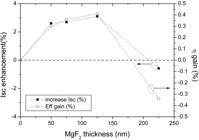 We practically applied the double ARC techniques in the 15.6 × 15.6 cm2 product class cells. The average efficiency of these mc-Si solar cells was larger than 16.2%. To prevent possible measured error, we produced five cells for each MgF2 coating thickness to obtain its average efficiency. Table 1 shows the three MgF2 thicknesses, 50, 60, and 75 nm, and the averaged data. Open circuit voltage (Voc) of these cells increased and the fill-factor (FF) decreased slightly, with little affect on efficiency. The efficiency gain results from increased Isc. Increasing the light coupled into the silicon causes the double ARC function to enhance silicon absorption Table 1 shows that the Isc and efficiency increased gradually when MgF2 thickness increased. The phenomena are similar with the results of Figs. 4 and 7. The double ARC with 75 nm MgF2 thickness achieved a high efficiency mc-Si solar cell at about 17.2%. Table 1AM1.5G solar simulator results of the mc-Si solar cell with MgF2/SiNx double ARC coating. MgF2-50 means that the 50 nm MgF2 is coated on the cell, and so on.
5.ConclusionsThis article reports high performance double ARC techniques for the mc-Si solar cell, by optimizing MgF2 thickness using the model simulation to gain photocurrent density. We also measured the photocurrent of the mc-Si solar cell to correspond with the simulation and obtained close qualitative results. Finally, this work promoted high efficiency production of the mc-Si solar cell, exceeding 17% to achieve 17.2%. AcknowledgmentsThe authors gratefully acknowledge funding from the Neo Solar Power Corporation and ITRI/MCL of Taiwan. (Project No. 7454R0M410). ReferencesH. F. W. Dekkers, F. Duerinckx, J. Szlufcik, and J. Nijs,
“Silicon surface texturing by reactive ion etching,”
Opto-Electron. Rev., 8
(4), 311
–316
(2000). Google Scholar
S. Chhajed, M. F. Schubert, J. K. Kim, and E. F. Schubert,
“Nanostructured multilayer graded-index antireflection coating for Si solar cells with broadband and omnidirectional characteristics,”
Appl. Phys. Lett., 93 251108
(2008). http://dx.doi.org/10.1063/1.3050463 Google Scholar
J. Y. Chyan, W. C. Hsu, and J. A. Yeh,
“Broadband antireflective poly-Si nanosponge for thin film solar cells,”
Opt. Express, 17
(6), 4646
–4651
(2009). http://dx.doi.org/10.1364/OE.17.004646 Google Scholar
H.-C. Yuan, V. E. Yost, M. R. Page, P. Stradins, D. L. Meier, and H. M. Branz,
“Efficient black silicon solar cell with a density-graded nanoporous surface: Optical properties, performance limitations, and design rules,”
Appl. Phys. Lett., 95 123501
(2009). http://dx.doi.org/10.1063/1.3231438 Google Scholar
J. H. Zhao, A. H. Wang, P. Campbell, and M. A. Green,
“A 19.8% efficient honeycomb multicrystalline silicon solar cell with improved light trapping,”
IEEE Trans. Electron Devices, 46 1978
–1983
(1999). http://dx.doi.org/10.1109/16.791985 Google Scholar
M. Lipinski, P. Zieba, S. Jonas, S. Kluska, M. Sokolowski, and H. Czternastek,
“Optimisation of SiNx:H layer for multicrystalline silicon solar cells,”
Opto-Electron. Rev., 12
(1), 41
–44
(2004). Google Scholar
P. K. Pal, S. K. Datta, K. Mukhopadhyay, and H. Saha,
“Role of antireflection coating in microgrooved silicon solar cells,”
Sol. Energy Mater. Sol. Cells, 43
(1), 1
–14
(1996). http://dx.doi.org/10.1016/0927-0248(95)00151-4 Google Scholar
H. Nagel, A. G. Aberle, and R. Hezel,
“Optimised antireflection coatings for planar silicon solar cells using remote PECVD silicon nitride and porous silicon dioxide,”
Prog. Photovoltaics, 7
(4), 245
–260
(1999). http://dx.doi.org/10.1002/(SICI)1099-159X(199907/08)7:4<245::AID-PIP255>3.0.CO;2-3 Google Scholar
S.-Y. Lien, D.-S. Wuu, W.-C Yeh, and J.-C. Liu,
“Tri-layer antireflection coatings (SiO2/SiO2–TiO2/TiO2) for silicon solar cells using a sol–gel technique,”
Sol. Energy Mater. Sol. Cells, 90
(16), 2710
–2719
(2006). http://dx.doi.org/10.1016/j.solmat.2006.04.001 Google Scholar
S.-C. Chiao, J.-L. Zhou, and H. A. Macleod,
“Optimized design of an antireflection coating for textured silicon solar cells,”
Appl. Opt., 32 5557
–5560
(1997). http://dx.doi.org/10.1364/AO.32.005557 Google Scholar
S. K. Dhungel, J. Yoo, K. Kim, S. Jung, S. Ghosh, and J. Yi,
“Double-layer antireflection coating of MgF2/SiNx for crystalline silicon solar cell,”
J. Korean Phys. Soc., 49 885
–889
(2006). Google Scholar
Y. Yamamoto, Y. Uraoka, and T. Fuyuki,
“Passivation effect of plasma chemical vapor deposited SiNx on single-crystalline silicon thin-film solar cells,”
Jpn. J. Appl. Phys., 42 5135
–5139
(2003). http://dx.doi.org/10.1143/JJAP.42.5135 Google Scholar
E. D. Palik, Handbook of Optical Constants of Solids II, Academic Press, New York
(1998). Google Scholar
D. H. Macdonald, A. Cuevas, M. J. Kerr, C. Samundsett, D. Ruby, S. Winderbaum, and A. Leo,
“Texturing industrial multicrystalline silicon solar cells,”
Sol. Energy, 76 277
–283
(2004). http://dx.doi.org/10.1016/j.solener.2003.08.019 Google Scholar
|