
|
|
1.IntroductionLight trapping in thin film silicon devices is a key element for achieving high efficiency.1 Commonly, light trapping is introduced by growing the silicon layers on a rough (or textured) transparent conductive oxide (TCO) surface: light is scattered to angles different from normal incidence at the rough interface between TCO and silicon, because of the refractive index mismatch between the two materials.2 This effect increases the light path and absorption in silicon leading to higher output currents. This approach has been applied successfully in thin film silicon technology in both substrate and superstrate configurations.3 The most widespread TCOs used for this purpose have been SnO2 or ZnO that spontaneously develop rough surfaces during chemical vapor deposition.4, 5 Alternatively, ZnO can be textured chemically after deposition.6 More recently, it has been proposed that the introduction of metal nanoparticles has the potential to further increase the short circuit current of thin film silicon devices; see for instance, Ref. 7 and references therein. Metal nanoparticles display a wide range of optical phenomena, going from enhanced localized absorption to scattering processes and antireflection properties.8 Depending on the particular application and the wavelength range, optimum positions within the solar cell structure have been identified. Especially, the insertion of metal nanoparticles at the rear side of the solar cell is considered a very promising route for higher efficiency because it avoids unwanted backscattering processes and parasitic absorptions.9, 10 Reports have indeed shown that it is possible to increase the short circuit current of amorphous single junction solar cells by embedding metal nanoparticles in the back reflector.11, 12 However, the baseline is often set to a flat reflector and the actual gain over standard high efficiency device structures (silicon growth on textured TCO) is not always clear. In this paper the effect of metal nanoparticles in the back reflector structure of single junction amorphous silicon solar cells and in the intermediate reflector of amorphous/microcrystalline silicon tandem cells is investigated. Those cell structures are compared to state-of-the-art devices grown in the superstrate configuration on textured substrates. The optical and electrical performances of the cells are discussed to identify gains and losses. 2.ExperimentalThin film silicon solar cells were grown in a superstrate configuration on commercially available glass/TCO substrates. The silicon layers were deposited by PECVD using hydrogen silane mixtures for the intrinsic layers and adding p and n dopant gases to form the doped layers at temperatures around 200°C. The back reflectors for single junction and tandem cells were obtained sputtering ZnO/Ag layers. In the case of the tandem structure, sputtered ZnO was used as an intermediate reflector. To form the metal nanoparticles the growth of ZnO for the back or intermediate reflector was interrupted and the samples transferred to an evaporation system where either a thin layer of Ag or Au was deposited. After annealing the samples at temperatures between 150°C and 200°C to form the nanoparticles,13 the samples were again transferred to the sputtering system to embed the metal layer in ZnO. Standard processing steps were then resumed to complete the solar cells. Figure 1 shows the transmission spectrum of a thin Ag layer deposited on glass before and after annealing. The striking difference between the two spectra is attributed to the coagulation of Ag to form nanoparticles during annealing and resulting in a strong absorption resonance appearing at a wavelength near 450 nm. Scanning electron images of the sample after annealing confirm the formation of Ag nanoparticles with an average lateral size of 50 to 100 nm. Fig. 1(a) Transmission spectrum of a 10-nm thick Ag film as deposited (red) and after annealing (blue and green) displaying the characteristic resonance around 400 nm. (b) Scanning electron microscopy picture of a sample after Ag annealing, the nanoparticle lateral size is typically between 50 and 100 nm. 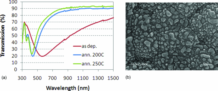 3.Amorphous Silicon Single JunctionsA sketch of the solar cell structure including metal nanoparticles is shown in Fig. 2. The solar cell is deposited in a superstrate configuration on glass/TCO substrate. After the deposition of the thin amorphous films by PECVD, ZnO is deposited on the rear side of the solar cell to form the negative contact. A thin layer of metal is evaporated on top of the back TCO layer and subsequently annealed at temperatures between 150°C and 200°C to form the nanoparticles. ZnO is deposited on top of the metal nanoparticles and thus forms the matrix where they are embedded. Finally, an Ag back reflector is applied to the solar cell. Figure 2 also shows the intended functionality of the metal nanoparticles: to increase the light scattering at the back reflector and improve the light trapping in the photoactive intrinsic amorphous silicon layer. Fig. 2Sketch of the layer structure of an amorphous silicon single junction solar cell containing metal nanoparticles embedded in the ZnO layer at the back of the solar cell. 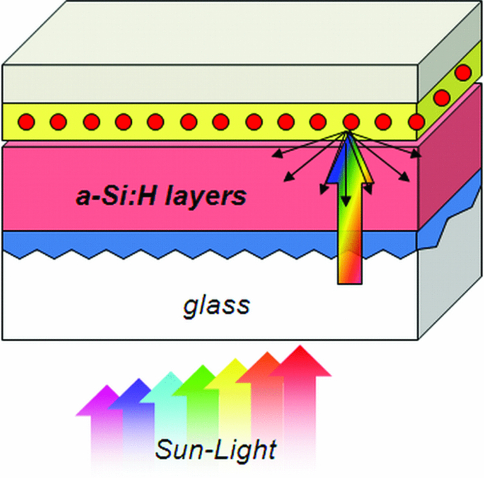 The performance of the solar cell structure sketched in Fig. 2 was compared to a solar cell obtained with a standard process. The only difference between the two was in the structure of the back reflector: for the standard (i.e., reference) solar cell the ZnO layer was deposited with the same thickness, but without interruption. The comparison between the two types of cells is displayed in Table 1. All solar cell parameters are renormalized to the standard process. After completion of the solar structure, the solar cell containing the nanoparticles shows a very poor performance and the output is reduced by almost one-third. It is necessary to perform an additional anneal to improve the electrical properties of the solar cell and to recover the open circuit voltage and fill factor of the reference sample. However, output current shows only a marginal increase upon annealing and therefore the efficiency is reduced by about 6% relative to the baseline process. Table 1Solar cell parameters for baseline process without nanoparticles (reference) and with nanoparticles. In the latter case, the results before and after solar cell annealing are reported.
This result, especially the reduction of short circuit current, is in stark contrast with the optical appearance of the solar cells. Upon visual inspection, the solar cells containing metal nanoparticles have a much darker appearance than the standard cell, similar to tandem thin film silicon devices. This indicates that the red part of the spectrum is absorbed by the nanoparticles. Figure 3 shows the striking difference between the optical appearances of modules processed according to the two described solar cell structures. It shows that the processing outlined for 1 cm2 lab cells can be easily upscaled to sizes used in production. Fig. 3Optical appearance of two large sized modules processed according to the solar cells compared in Table 1. The standard module is visible in the front and the module containing nanoparticles in the back reflector is placed in the background of the picture. 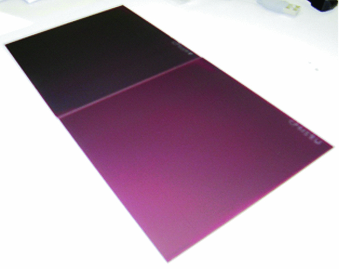 4.Amorphous/Microcrystalline Silicon Tandem JunctionsThe same stack of layers to form the amorphous silicon solar cell and the metal nanoparticles in the back ZnO matrix was used to investigate the effect of the scattering and absorption in an amorphous/microcrystalline tandem device. Figure 4 presents a sketch of such a structure. After preparing the amorphous top cell, the ZnO layer incorporating the metal nanoparticles was prepared. This layer now acts as an intermediate reflector between top amorphous subcell and bottom microcrystalline subcell. Subsequently, a sequence of microcrystalline silicon layers was applied to form the bottom subcell, ZnO to form the negative contact and an Ag back reflector. No metal nanoparticles were incorporated in the back reflector of the solar cell. In Fig. 4, a cross-sectional transmission electron microscopy image of a tandem solar cell shows the metal nanoparticles formed after annealing embedded in the interlayer. Fig. 4(a) Sketch of the layer structure of an amorphous/microcrystalline tandem cell incorporating metal nanoparticles in a ZnO layer placed between the two subcells. (b) Transmission electron microscopy image of a cross-sectional view of the tandem solar cell, showing the metal nanoparticles embedded in the ZnO interlayer. 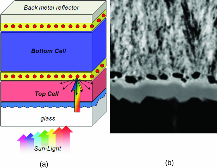 The purpose of this structure is again to evaluate the effectiveness of metal nanoparticles incorporated in a ZnO matrix to improve the backreflection of light in the top cell. Intermediate reflectors have proven to be effective in increasing the short circuit current in the amorphous top cell, by partially reflecting light back into the top layers.14 As a reference cell for comparison, the same cell structure was used except for the incorporation of nanoparticles in the intermediate reflector. Figure 5 shows an interesting result comparing the spectral response of the tandem cell containing the nanoparticles embedded in the interlayer with the one obtained for the reference cell and standard interlayer. Remarkably, an increase can be observed in the spectral range from 500 to 700 nm, indicating a gain in top cell current by using the innovative interlayer containing the metal nanoparticles. In this particular case the metal used was Ag with an initial (before annealing) thickness of approximately 10 nm. This result is in agreement with simulations carried out for a very similar solar cell structure.15 In that case, the authors attributed the effect to an increased back-reflection from the interlayer with metal nanoparticles embedded in ZnO compared to a standard ZnO interlayer. From this analysis it can be concluded that nanoparticles embedded in an intermediate reflector are indeed effective in increasing the backscattering of light in this wavelength range. This result is in contrast with the experiments on amorphous single junction solar cells, where a decrease of current output was observed. The reasons for this are not clear at this stage. However, the fact that the nanoparticles are embedded within the solar cell structure, distant from the Ag back reflector, might affect the light scattering and absorption phenomena.16 Fig. 5Comparison between the spectral response measured for top cells incorporating metal nanoparticles in the intermediate reflector (green curve) and a standard ZnO intermediate reflector (black curve). 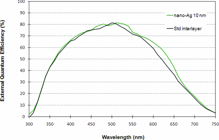 Figure 6 displays the spectral response of amorphous/microcrystalline tandem cells incorporating different types of intermediate layers. The curve between 300 and 700 nm relates to the spectral response of the amorphous top-cell, while the curve between 500 and 1100 nm is related to the spectral response of the microcrystalline bottom cell. Like in single junction amorphous cells, the increase in spectral response observed for a thin Ag layer deposited can be reproduced for different thicknesses as shown by the blue curve in Fig. 6. The gain between 550 and 700 nm is attributed to the enhanced backscattering of the intermediate reflector containing nanoparticles, whereas the larger response at shorter wavelength is due to slight optical changes in the first layers of the solar cell. They are not concerned by this discussion, because these wavelengths are typically absorbed in a single pass through the amorphous layer. The green and black curves reproduce the results already displayed in Fig. 5. In addition, the red curve shows the spectral response of a tandem cell without intermediate reflector. Fig. 6Spectral response of tandem devices with intermediate reflectors containing Ag nanoparticles. Comparison with a tandem cell with standard interlayer and without interlayer is also shown. 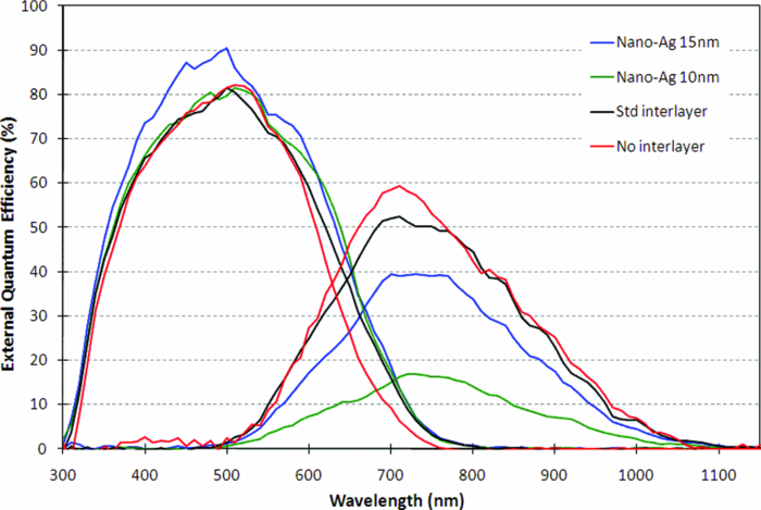 The gain in spectral response compared to this baseline is clear for all tandem devices with intermediate reflector. Figure 6 also reproduces the spectral response of the bottom cells. The impact of the incorporation of metal nanoparticles is quite severe on the red and infrared part of the solar spectrum. The loss of quantum efficiency for tandem devices with metal nanoparticles compared to those without is evident. The origin of this loss is preferentially to be attributed to optical factors, mainly parasitic absorption and not to charge collection losses, since the electrical parameters of the solar cells (like open circuit voltage and fill factor) are comparable to the reference device. Table 2 shows the solar cell parameters, normalized to the values of a reference device with intermediate reflector containing no metal nanoparticles. Independent of the types of metals used (Ag and Au), comparable open circuit voltages and fill factors could be obtained, while the short circuit current was reduced by the poor spectral response of the bottom cells. Table 2Solar cell parameters for tandem solar cells incorporating metal nanoparticles in intermediate reflectors. All values are normalized to a reference cell with standard intermediate reflector.
The blue and green curves in Fig. 6 are for samples with the same layer structure, but with different Ag thicknesses. The comparison between the spectral response of the bottom cells shows that the initial metal thickness has an important impact on the reduction of the signal from the bottom cell. A 15-nm thick layer subsequently annealed leads to a much better response compared to the case with 10 nm Ag. Figure 7 shows the normalized efficiency of thin film silicon tandem devices with metal films in the intermediate reflector. Au and Ag were used as metals and different thicknesses were deposited. A clear trend is visible as a function of thickness: for Au nanoparticles the optimum is very narrow and located around 10 nm, whereas for Ag nanoparticles a weak dependence on film thickness is observed. Efficiency is mainly affected by the short circuit current and detailed analysis (not shown) proves that the spectral response of the bottom cell limits the output current of the tandem solar cell. Overall, similar optimum efficiencies were obtained with the two metals. Fig. 7Tandem solar cell efficiency versus thickness of the as-deposited metal film in the intermediate reflector. Ag and Au have been used as metals. 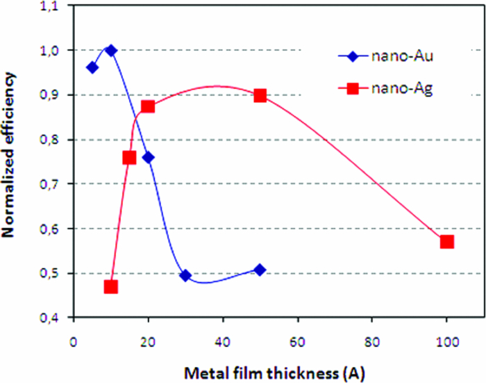 These experimental results indicate that the formation dynamics of the metal nanoparticles has a direct and important impact on the solar cell performance. At this stage it is not clear what the cause for this is, however, precise control of the size and possibly shape of the nanoparticles appear important parameters for device optimization. Further investigations will be needed to confirm and clarify these points. 5.ConclusionsSingle junction thin film silicon devices incorporating metal nanoparticles in the back reflector structure display comparable electrical solar cell parameters than reference solar cell with a standard structure. In addition, the optical appearance of these cells confirms the increased light trapping in the device. However, the short circuit current of the devices is reduced below the values of the reference cell indicating that parasitic absorption processes related to the metal nanoparticles have a larger strength than backscattering processes in the active layer. In the case of amorphous/microcrystalline tandem devices, metal nanoparticles are incorporated in the intermediate reflector. In this case, the spectral response of the top amorphous subcells displays an increase in the wavelength region between 500 and 700 nm compared to a structure with a standard interlayer. This indicates a positive contribution of backscattering processes. However, a strong parasitic absorption is visible in the larger wavelength region, severely affecting the spectral response of the microcrystalline bottom subcell. Open circuit voltages and fill factors are comparable to a reference tandem cell; however, the efficiency is lower due to the reduced output current. The negligible impact of metal nanoparticles on the electrical parameters of the thin film silicon solar cells is an encouraging feature. In conjunction with the trends observed on tandem solar cells with variable as-deposited metal thicknesses, the results presented in this paper suggest that careful tailoring of the metal nanoparticle size and shape could be an effective approach to improve the efficiency of a thin film silicon device incorporating metal nanoparticles. AcknowledgmentsThe authors acknowledge financial support of the New Energy and Industrial Technology Development Organization (NEDO) under the Ministry of Economy, Trade and Industry (METI). ReferencesK. Yamamoto,
“Very thin film crystalline silicon solar cells on glass substrate fabricated at low temperature,”
IEEE Trans. Electron Devices, 46 2041
–2047
(1999). http://dx.doi.org/10.1109/16.791994 Google Scholar
A. Shah, P. Torres, R. Tscharner, N. Wyrsch, and H. Keppner,
“Photovoltaic technology: The case for thin-film solar cells,”
Science, 285 692
–698
(1999). http://dx.doi.org/10.1126/science.285.5428.692 Google Scholar
A. Shah, H. Schade, M. Vanecek, J. Meier, E. Vallat-Sauvain, N. Wyrsch, U. Kroll, C. Droz, and J. Bailat,
“Thin-film silicon solar cell technology,”
Prog. Photovoltaics, 12 113
–142
(2004). http://dx.doi.org/10.1002/pip.533 Google Scholar
S. Faÿ, L. Feitknecht, R. Schlüchter, U. Kroll, E. Vallat-Sauvain, and A. Shah,
“Rough ZnO layers by LP-CVD process and their effect in improving performances of amorphous and microcrystalline silicon solar cells,”
Sol. Energy Mater. Sol. Cells, 90 2960
–2967
(2006). http://dx.doi.org/10.1016/j.solmat.2006.06.003 Google Scholar
M. Kambe, M. Fukawa, N. Taneda, and K. Sato,
“Improvement of a-Si solar cell properties by using SnO2:F TCO films coated with an ultra-thin TiO2 layer prepared by APCVD,”
Sol. Energy Mater. Sol. Cells, 90 3014
–3020
(2006). http://dx.doi.org/10.1016/j.solmat.2006.06.008 Google Scholar
J. Müller, G. Schöpe, O. Kluth, B. Rech, V. Sittinger, B. Szyszka, R. Geyer, P. Lechner, H. Schade, M. Ruske, G. Dittmar, and H.-P. Bochem,
“State-of-the-art mid-frequency sputtered ZnO films for thin film silicon solar cells and modules,”
Thin Solid Films, 442 158
–162
(2003). http://dx.doi.org/10.1016/S0040-6090(03)00964-7 Google Scholar
H. A. Atwater and A. Polman,
“Plasmonics for improved photovoltaic devices,”
Nature Mater., 9 205
–213
(2010). http://dx.doi.org/10.1038/nmat2629 Google Scholar
K. R. Catchpole and A. Polman,
“Plasmonic solar cells,”
Opt. Express, 16 217
–218
(2008). http://dx.doi.org/10.1364/OE.16.021793 Google Scholar
S. Pillai, K. R. Catchpole, T. Trupke, and M. A. Green,
“Surface plasmon enhanced silicon solar cells,”
J. Appl. Phys., 101 093105
(2007). http://dx.doi.org/10.1063/1.2734885 Google Scholar
T. L. Temple, G. D. K. Mahanama, H. S. Reehal, and D. M. Bagnall,
“Influence of localized surface plasmon excitation in silver nanoparticles on the performance of silicon solar cells,”
Sol. Energy Mater. Sol. Cells, 93 1978
–1985
(2009). http://dx.doi.org/10.1016/j.solmat.2009.07.014 Google Scholar
P. Q. Luo, E. Moulin, J. Sukmanowski, F. X. Royer, X. M. Dou, and H. Stiebig,
“Enhanced infrared response of ultra thin amorphous silicon photosensitive devices with Ag nanoparticles,”
Thin Solid Films, 517 6256
–6259
(2009). http://dx.doi.org/10.1016/j.tsf.2009.02.060 Google Scholar
F. J. Haug, T. Soederstroem, O. Cubero, V. Terrazzoni-Daudrix, and C. Ballif,
“Plasmonic absorption in textured silver back reflectors of thin film solar cells,”
J. Appl. Phys., 104 064509
(2008). http://dx.doi.org/10.1063/1.2981194 Google Scholar
J. Okumu, C. Dahmen, A. N. Sprafke, M. Luysberg, G. von Plessen, and M. Wuttig,
“Photochromic silver nanoparticles fabricated by sputter deposition,”
J. Appl. Phys., 97 094305
(2005). http://dx.doi.org/10.1063/1.1888044 Google Scholar
K. Yamamoto, A. Nakajima, M. Yoshimi, T. Sawada, S. Fukuda, T. Suezaki, M. Ichikawa, Y. Koi, M. Goto, T. Meguro, T. Matsuda, M. Kondo, T. Sasaki, and Y. Tawada,
“A thin-film silicon solar cell and module,”
Prog. Photovoltaics, 13 489
–494
(2005). http://dx.doi.org/10.1002/pip.645 Google Scholar
S. Fahr, C. Rockstuhl, and F. Lederer,
“Metallic nanoparticles as intermediate reflectors in tandem solar cells,”
Appl. Phys. Lett., 95 121105
(2009). http://dx.doi.org/10.1063/1.3232230 Google Scholar
F.-J. Haug, T. Söderström, O. Cubero, V. Terrazzoni-Daudrix, and C. Ballif,
“Influence of the ZnO buffer on the guided mode structure in Si/ZnO/Ag multilayers,”
J. Appl. Phys., 106 044502
(2009). http://dx.doi.org/10.1063/1.3203937 Google Scholar
|


