|
|
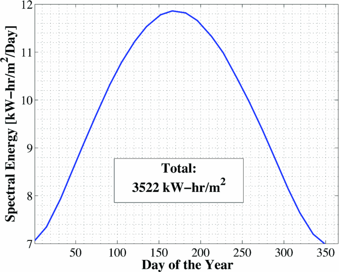
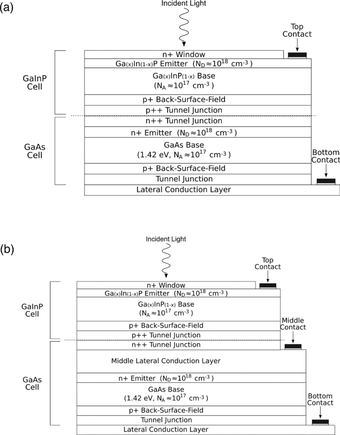
1.IntroductionSolar concentrator cells are typically designed for maximum efficiency under a reference solar spectrum, such as AM1.5d,1 which represents an average direct irradiance under reasonable, cloudless atmospheric conditions. This methodology is sensible, as most of these systems have been designed with the goal of achieving record efficiency and must be easily compared to cells produced by other laboratories. More practically, the design goals should include achieving maximum energy production over the course of a day, month, or year, depending upon the application. The resulting differences in cell design, primarily found in absorber layer thickness and bandgap choices, between these two different goals stems from variations in the energy distribution of the solar spectra in the morning (or evening) versus solar noon, and in the summer versus the winter, which is due largely to a change in relative air mass.2 An example of this can be seen in solar spectra for Las Vegas, Nevada. Simulated solar spectra were generated for Las Vegas, Nevada from sunrise to sunset, 2 days per month (1st and 15th) in 10 min increments using MODTRAN (MODerate resolution atmospheric TRANsmission);3, 4 direct irradiance was assumed. These spectra represent a wide range of the relative air mass that may be seen by a solar cell over the course of the day or year, as will be shown in Fig. 13. Weather effects, such as cloud cover, were not included in the spectra, and the aerosol model was assumed equal at each location. Spectra at solar-noon on June 15th and December 15th, along with the standard AM1.5d spectrum, are shown in Fig. 1. Fig. 1Direct normal spectral irradiance at solar noon in Las Vegas, Nevada on June 15th and December 15th, and AM1.5d. 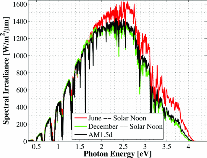 Fig. 13Normalized solar spectra on June 15th at 7:00 a.m. and solar-noon and on December 15 at solar-noon. 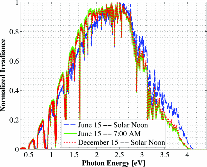 Figure 1 illustrates the decrease in absolute spectral power and reduction in the spectral energy content of the high photon energy portion of the solar spectrum that results from the increased air mass in December versus June.2 A similar pattern is observed when comparing spectra in the morning (or evening) and solar-noon. The variation in direct normal spectral power over the course of the day in Las Vegas, Nevada on June 15th and December 15th is shown in Fig. 2. Fig. 2Direct normal spectral power on June 15th and December 15th over the course of the day in Las Vegas, Nevada. 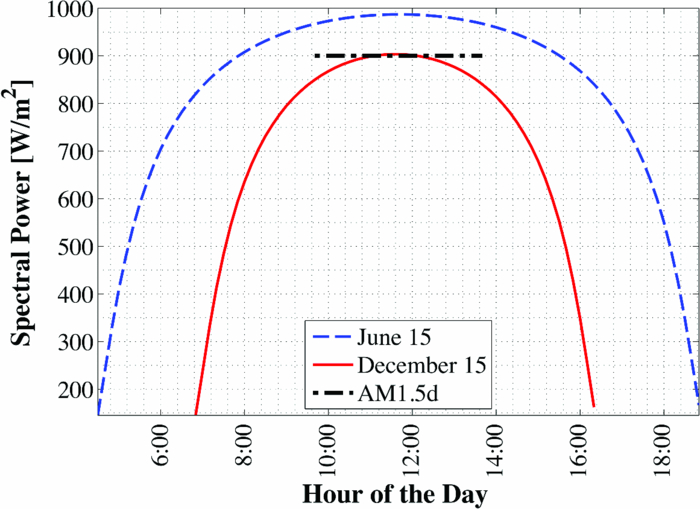 Less spectral power is available in December than in June at all times of the day, and thus less total daily energy is incident in December versus June. This is illustrated in Fig. 3, which shows the available spectral energy over the course of the entire year in Las Vegas, Nevada. Figures 1, 2, 3 suggest that designing a cell or system for maximum energy production has the potential to require that it be optimized using a nonstandard solar spectrum, as has been suggested by Kinsey and Edmondson.5 Initial simulation results were reported by Haas6 and showed that maximum yearly energy is produced for a two-terminal GaInP/GaAs tandem installed in Las Vegas, Nevada by designing for a mid-November, solar-noon spectra. This work will extend the initial results by employing more comprehensive models and by looking at daily and monthly energy production, in addition to yearly energy production. Though many recent world record multijunction tandems utilize three or more junctions,7 GaInP/GaAs tandems are employed as an important component of many spectrally spit systems,8, 9, 10 and thus the study of these dual junction devices is still useful. Simple ideal-diode models developed using detailed-balance, as formulated by Shockley and Quiesser,11 have often been used in choosing optimal solar cell bandgaps for maximum yearly energy production.2, 12, 13 However, the results achieved in this way may only loosely correlate with actual cell performance because the specifics of the cell layer structure and recombination play a significant role in determining the optimal cell design. Detailed numerical models, which numerically solve Poisson's equation and hole and electron continuity assuming drift and diffusion based transport, are better tools for this sort of analysis as the specifics of cell structure can easily be incorporated. Detailed numerical models are employed in this work to optimize a GaInP/GaAs tandem for maximum energy production in two- and three-terminal configurations via the GaInP bandgap and GaInP and GaAs absorber layer thicknesses. A comparison of the results achieved using these detailed models to those found using a simpler model shows that while the simple model shows similar trends, it cannot correctly predict the optimal design parameters unless a more complicated formulation, such as Hovel's equations,14, 15 are employed. However, these models also make several simplifying assumptions about carrier recombination and material quality16 that are not assumed in a detailed numerical model. It will be shown that designing for the AM1.5d standard spectrum yields a tandem that produces nearly maximum yearly energy for all of the geographical locations considered in this work. This result is independent of the optical concentration, up to at least 500 suns. 2.Methods2.1.Detailed Numerical Modeling2.1.1.Tandem layer structure and material parametersThe tandem layer structure in both two- and three-terminal configurations, shown in Fig. 4, follows that proposed by Gray17 The underlying structure is general enough that the conclusions drawn from the simulation results can also be applied to other GaInP/GaAs systems. One-dimensional detailed numerical models for the GaInP and GaAs sub-cells were developed in ADEPT (Ref. 18) by partitioning the tandem at the tunnel junction, as implied by Fig. 4, and simulating each independently (the characteristics are later combined to determine the performance of the tandem in a two-terminal configuration). This assumes a high quality tunnel-junction with very low effective series resistance under forward bias. In this work it is assumed that the peak current is not exceeded so that this assumption remains valid. This assumption is reasonable, as tunnel junctions with peak tunneling currents exceeding 600 A/cm2 have been grown in similar multijunction devices.19 2.1.2.Material parametersWhile numerous design parameters affect device performance, the cell optimization procedure utilized in this work considers only the GaInP and GaAs sub-cell base layer thicknesses and the GaInP bandgap as available design variables. It is assumed that the material parameters do not vary with layer thickness; however, several important material parameters are strongly dependent upon the GaInP alloy composition, and thus its bandgap. The variation of these parameters with bandgap must be quantified to accurately model device performance. Determining a reasonable variation of Ga(x)In(1−x)P bandgap, Eg, with Ga composition, x, is problematic as Eg is very sensitive to crystal ordering,20 which is determined by the processing conditions such as growth rate and temperature:21 GaInP grown with the same Ga composition but under different conditions may vary in bandgap by nearly 100 MeV. Alibert22 developed expressions for the direct and indirect bandgaps of GaInP versus Ga composition based upon electroreflectance measurements; however, the direct gap predicted by these expressions is nearly 50 MeV greater than what is used in modern GaInP-based solar cells. Thus, as a means of approximating the dependence of Eg on x for modern GaInP without considering the crystal ordering, a least-squares fitting scheme was used in conjunction with bandgaps from published GaInP solar cells, as well as the known bandgaps of InP (x = 0, Eg = 1.344 eV) and GaP (x = 1, Eg = 2.26 eV). The result of this approximation is shown in Fig. 5. The form of the least-squares fit is given in Eq. 1. [TeX:] \documentclass[12pt]{minimal}\begin{document}\begin{equation}
E_g (x) = - 0.2722x^2 + 1.1925x - 1.3399.
\end{equation}\end{document} It is assumed that the band structure in the range of interest (1.82 and 1.98 eV) is similar enough to the ≈1.89 eV case so that an assumed set of absorption coefficients, α (λ) (based upon a concatenation of coefficients published by Schmiedel31 and Kurtz16), at this bandgap can be shifted up and down in energy to obtain the absorption coefficients throughout the range of interest.Fig. 5Least-squares curve-fit to published GaInP solar cell bandgaps (Refs. 21, and 23, 24, 25, 26, 27), and the bandgaps of InP and GaP (Refs. 28, 29, 30). 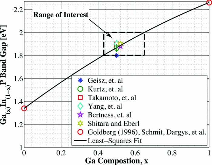 Variation in the dielectric constant, ɛs, and electron affinity, χ, with composition follow the known forms32 given by Eqs. 2, 3, where x is found using Eq. 1. [TeX:] \documentclass[12pt]{minimal}\begin{document}\begin{equation}
\varepsilon _s (x) = 12.5 - 1.4x,
\end{equation}\end{document}
[TeX:] \documentclass[12pt]{minimal}\begin{document}\begin{equation}
\chi (x) = 4.38 - 0.58x.
\end{equation}\end{document} Known forms could not be found for the variation of the Auger and radiative recombination coefficients (Λn, Λp, and A0, respectively) with x or Eg. However, known Auger coefficients at x = 0, 0.51, and 1 suggest a maximum between x = 0 and x = 1. Additionally, the radiative coefficient is expected to be proportional to [TeX:] $E_g^2$ (Ref. 33). Thus, both coefficients were fit to quadratic forms using known values at x = 0, 0.51, and 1 (Refs. 28, 29, 30, 32). Again, due to a lack of available data, it has been assumed that the Auger recombination coefficient for electrons and holes is identical; thus, Λn = Λp = Λ. Equations 4, 5 give the least-squares curve-fit forms for the Auger and radiative recombination coefficients, respectively. [TeX:] \documentclass[12pt]{minimal}\begin{document}\begin{equation}
\Lambda (x) = - 8.2 \times 10^{ - 30} x^2 + 8.3 \times 10^{ - 30} x + 9 \times 10^{ - 31},
\end{equation}\end{document}
[TeX:] \documentclass[12pt]{minimal}\begin{document}\begin{equation}
A_0 (E_g) = - 2.362 \times 10^{ - 10} E_g^2 + 7.202 \times 10^{ - 10} E_g - 4.214 \times 10^{ - 10}.
\end{equation}\end{document} The effective density of states in the conduction band and valence band, NC and NV, respectively, vary with the effective carrier masses as given by Eqs. 6, 7. [TeX:] \documentclass[12pt]{minimal}\begin{document}\begin{equation}
N_C = ({2\pi qkTm_e^* /h^2 })^{3/2},
\end{equation}\end{document}
[TeX:] \documentclass[12pt]{minimal}\begin{document}\begin{equation}
N_V = ( {2\pi qkTm_h^* /h^2 })^{3/2}.
\end{equation}\end{document} The effective electron and hole masses, m∗e and m∗h, respectively, vary with composition. A known dependence of m∗h on x was found;32 however, a known variation of m∗e with x could not be obtained. Consequentially, m∗e(x) was again approximated using a quadratic least-squares curve-fit with known values at x = 0, 0.51, and 1 (Refs. 28, 29, 30, 32). m∗e(x) and m∗h(x) are given in Eqs. 8, 9. [TeX:] \documentclass[12pt]{minimal}\begin{document}\begin{equation}
m_e^* (x)/m_0 = 0.0254x^2 - 0.114x + 0.08,
\end{equation}\end{document}
[TeX:] \documentclass[12pt]{minimal}\begin{document}\begin{equation}
m^* _h (x){\rm }/m_0 = 0.19x + 0.6.
\end{equation}\end{document} To verify the calculated values of NC and NV, the intrinsic carrier concentration, ni, was extracted as [TeX:] \documentclass[12pt]{minimal}\begin{document}\begin{equation}
n_i = \sqrt {N_C N_V } \exp [ - E_g /2kT]
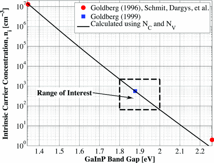
\end{equation}\end{document} and compared to known values. This comparison is shown in Fig. 6; the extracted and known values of ni agree very well.Data regarding the variation of the Shockley–Read–Hall (SRH) recombination lifetimes for holes and electrons, τn and τp, respectively, and of the hole and electron mobilities, μn and μp, respectively, with Ga composition were not found. Thus, these parameters were set at reasonable values based upon the majority carrier doping for each layer. It was assumed that the majority and minority carrier SRH lifetimes were equal in all layers, again due to the lack of available data. This assumption should not affect the results of this work significantly as it was verified that even up to 500 suns optical concentration, the quasineutral regions do not enter a high-level injection condition. All SRH recombination was assumed to occur in a single-level, midgap trap. The noncomposition-varying GaInP sub-cell material parameters used in the simulation are summarized in Table 1. Table 1Noncomposition-varying GaInP sub-cell material parameters.
The front and back surface minority carrier recombination velocities, SF and SB, respectively, were used as boundary conditions. However, the detailed numerical models employed in this work are one-dimensional, and thus these recombination velocities must act as averages or effective velocities that account for variation in the true recombination velocities across the surface area of the cell. At the front surface of the GaInP cell, SF accounts for the minority carrier surface recombination velocity at the window/electrode interface, which is expected to be nearly the thermal velocity (≈107 cm/s) due to the presence of an ohmic contact, and the window/antireflection coating (ARC) interface, which is expected to be somewhat lower.37 Previous modeling of this particular structure indicated that SF = 9.5 × 105 cm/s allowed for good matching of the modeled and measured external quantum efficiency (EQE) in the high photon energy range where the effect of the front surface is important. One would expect that the effective minority carrier front surface recombination velocity should vary with applied bias;38 however, in this work it is assumed that the effect of this variation is small enough that SF at the front surface may be held constant. At the back of the tandem and at the interface between sub-cells, the effective minority carrier recombination velocity is expected to be very close to the thermal velocity across the entire cell area due to the presence of tunnel junctions, which act like ohmic contacts. The minority carrier recombination velocities at these interfaces were thus set to 107 cm/s. Of course, the models assume high quality window and back-surface-field (BSF) layers; thus, the minority carrier recombination velocities at the window/emitter interface and base/BSF interface, which most strongly effect device performance, were effectively very low. These recombination velocities were calculated for a representative case at the maximum power point (a tandem optimized for the June 15th solar noon spectra, operating under the June 15th solar noon spectra) and were found to be 131 cm/s at the window/emitter interface and 3450 cm/s at the base/BSF interface. In this work it is assumed that the bandgap of the GaAs material remains at 1.42 eV. Fortunately, GaAs is very well characterized. The material parameters used for the GaAs sub-cell are summarized in Table 2. Table 2GaAs sub-cell material parameters. Note that the long SRH lifetime was chosen to ensure radiative-limited recombination, as suggested by Lush (Ref. 39). The assumed absorption coefficients are based upon a concatenation of coefficients published by Casey (Ref. 40).
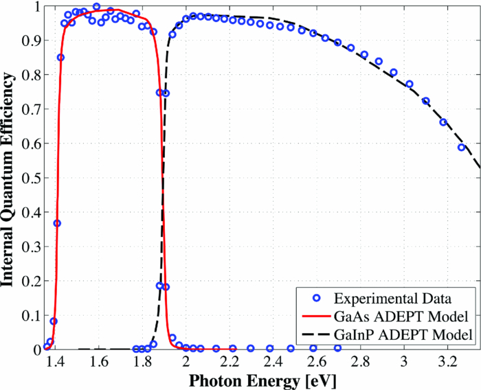
The bandgap of the middle-conducting-layer (MLCL) in the three-terminal configuration was assumed to be 30 MeV larger than the GaInP layers in the top sub-cell to reduce any potential absorption in this layer. Additionally, the bandgap and electron affinity of the GaInP sub-cell back-surface field were chosen to ensure a large (>0.4 eV) energy barrier to minority carrier electrons in the sub-cell base, regardless of the GaInP bandgap. Simulations showed that the maximum possible additional generation due to radiative coupling from the top sub-cell to the bottom constitutes less than 0.5% of the tandem Jsc near the operating point, and thus it was ignored. Finally, it is assumed that both junctions remain at room temperature, as this temperature could vary significantly depending upon the assumed thermal system. 2.1.3.Model verificationBecause the conclusions drawn from this work are based upon numerical simulations, it is necessary to validate the models against measured cell data. Internal quantum efficiency (IQE) is an excellent verification characteristic because it includes information about the type and location of the various recombination mechanisms and is thus a good indication of how well the physics of the model matches the actual cell. The measured tandem (similar to the three-terminal tandem reported on by Gray17) uses the three-terminal tandem structure shown in Fig. 4. The material parameters used in the simulation follow those discussed earlier for a GaInP bandgap of ≈1.9 eV, except that the GaInP emitter SRH lifetime was set at 0.2 ns. The measured46 and modeled IQE for both sub-cells is shown in Fig. 7. The model is a good fit to the data. 3.Theory/Calculations3.1.Simulation Methodology3.1.1.Procedure for the simultaneous optimization of the GaInP bandgap and GaInP and GaAs base layer thicknessesAs the bandgap of the GaInP sub-cell is reduced, the current available to it increases; however, carriers are also collected at a lower voltage. Similarly, increasing the thickness of a sub-cell increases the number of photons that are absorbed, but at the expense of increased recombination. The current-matching constraint in the two-terminal configuration further complicates these trade-offs. Due to the strong interaction between these three parameters, the optimal GaInP bandgap and GaInP and GaAs base layer thicknesses is computed simultaneously. A brute-force optimization scheme is utilized in this work in which every combination these three parameters (over a predefined range) are simulated to find the optimal combination for a particular spectrum. The GaInP bandgap was varied from 1.82 to 1.98 eV, the GaInP base layer thickness was varied from 0.1 to 5 μm, and the GaAs base layer thickness was varied from 1 to 6 μm. While GaInP with a bandgap of 1.98 eV would be severely lattice mismatched with GaAs, it will be shown that the optimal GaInP bandgap for all of the spectra considered was less than ≈1.91 eV, which can be grown lattice-matched to GaAs.47 A perfect ARC was assumed in all cases. Two-dimensional effects, such as dark-diode losses due to nonilluminated cell area (see Fig. 4) and joule losses due to lateral current flow in the emitter and MLCL were also ignored. While including these losses would provide a better estimate of actual device performance, the effect would be nearly the same for all tandem designs and thus would not change the final conclusions. An optical concentration of 33 suns has been employed. The effect of concentration will be further discussed in Sec. 5.2. It is assumed that optically concentrating the incident spectrum only scales the spectra by the concentration ratio and does not change the relative distribution of spectral energy. The result of this simulation method for optimization under the June 15th, solar-noon spectrum is shown for the two- and three-terminal configurations in Fig. 8. Fig. 8Maximum power output of two- and three-terminal tandem designs with optimal GaInP and GaAs sub-cell base thicknesses for various GaInP bandgaps at solar-noon on June 15th in Las Vegas, Nevada. 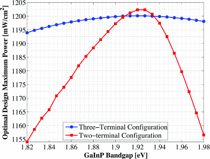 The two-terminal configuration is more sensitive to GaInP bandgap than the three-terminal configuration due to the requirement of current-matching. Additionally, the peak power output in the two-terminal configuration exceeds that of the three-terminal configuration as a result of some parasitic absorption and recombination in the MLCL. The roughness in the curve at low bandgap is due to the high degree of sensitivity of the tandem to the GaInP sub-cell thickness and limitations imposed by the numerical optimization procedure. The shape and overarching behavior of the remaining monthly optimized designs (for the 15th of each month) is very similar to the June case shown in Fig. 8, though the optimal GaInP bandgap and the maximum power generated at this point varies. The power output of the tandem is also sensitive to the GaInP and GaAs sub-cell base thicknesses. However, it was found that for the assumed GaAs and GaInP material parameters (recombination parameters and absorption coefficients in particular), the optimal GaAs sub-cell base thickness is ≈4.5 to 4.7 μm in all cases, and that the power output is highly insensitive to this thickness down to ≈3.5 μm. Thus, for the remainder of this work it is assumed that in all cases the GaAs sub-cell base thickness is set to the optimum value for each design spectrum, and it is understood that in a real device the GaAs base would likely be grown thinner to reduce cost. A contour plot showing the variation in maximum power output with GaInP Eg and the GaInP sub-cell base thickness for the June 15th optimization, normalized by the peak value, is shown for both configurations in Fig. 9. Fig. 9Variation in maximum power output with GaInP Eg and the GaInP sub-cell base thickness for the June 15th optimization, normalized by the peak value (shown as a white dot). Note the difference in color scale between the two plots. (a) Two-terminal configuration, (b) three-terminal configuration. 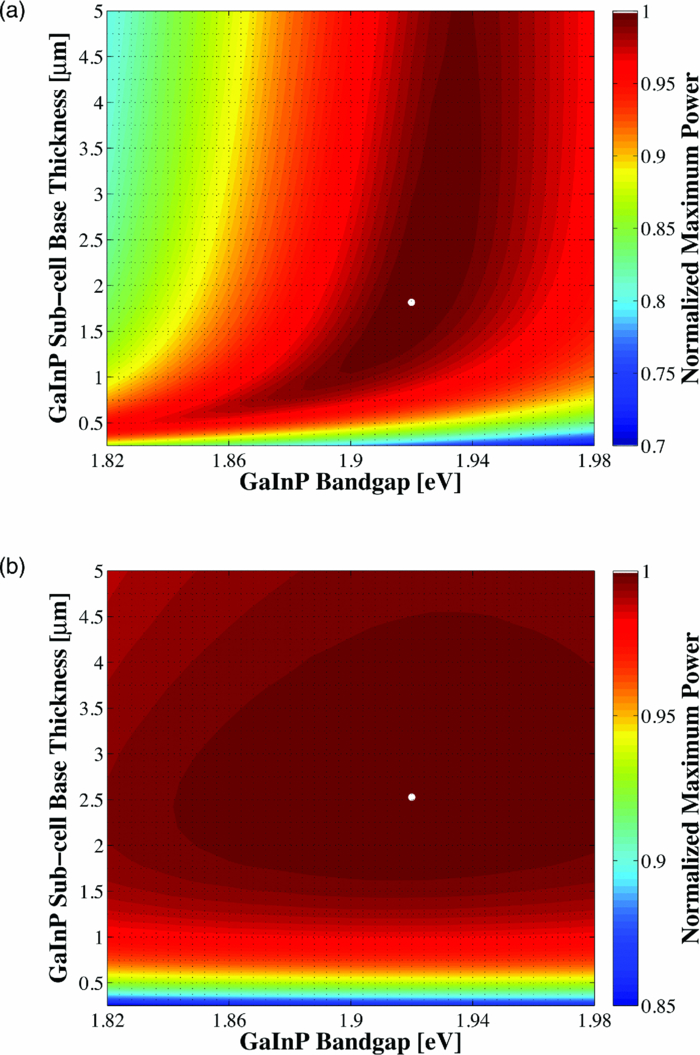 The remaining designs for each monthly spectrum show similar behavior, with the optimal GaInP sub-cell base thickness ≈1.7 to 2.6 μm. Again, this optimal thickness is sensitive to the assumed recombination lifetimes and absorption coefficients, and is thicker than many GaInP sub-cell base layers, which are typically in the range of 0.5 to 1.5 μm.24, 26, 48, 49 The optimal sub-cell base thickness for a given GaInP Eg is determined by three factors: the increase in carrier generation with increasing base thickness, the increase in carrier recombination with base thickness, and the variation in the sub-cell current matching condition, which only applies to the two-terminal case. The role of carrier generation may be captured by Jinc, the maximum possible short-circuit current for a given thickness and Eg. Similarly, the increase in carrier recombination with base thickness is encapsulated in the calculated collection efficiency, which is defined as the ratio of collected to generated minority carriers. The variation in these parameters for the June 15th two-terminal optimization is shown in Fig. 10. Fig. 10Variation in Jinc (normalized by a value at 10 μm), collection efficiency, and relative sub-cell current mismatch for the June 15th two-terminal design at the optimal GaInP Eg. 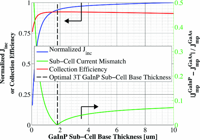 It is clear from Fig. 10 that a primary factor in setting the optimal GaInP base thickness in the two-terminal configuration is the sub-cell current matching condition (in the three-terminal configuration it is simply a compromise between generation and collection). Figure 10 also illustrates how the current matching requirement causes the high degree of sensitivity of the tandem to the GaInP thickness in the two-terminal case shown in Fig. 9. The optimization procedure discussed here was repeated for solar-noon spectra on the 15th of each month in addition to the AM1.5d standard spectrum. The behavior of each design with respect to the GaInP bandgap and GaInP sub-cell base layer thickness is very similar to that shown in Figs. 9, 10, though the optimal values vary. The daily energy production of each of the 13 optimized designs is calculated by simulating over the course of the day, twice per month (the 1st and 15th) in 10 min increments, and then summing the contribution of each by assuming constant energy production during the 10 min increments. The monthly and yearly energy production is calculated by assuming constant energy production throughout each 2 week period between simulation days. 3.1.2.Justification of the optimization methodologyThe optimization procedure was limited to finding the best combination of GaInP bandgap and GaInP and GaAs base layer thicknesses for a set of incident spectra with all other design parameters fixed. However, the power output of the tandem in each case depends on numerous other parameters in addition to those utilized in this work. For example, doping density, particularly in the emitter and base layers, affects Voc, both because the SRH lifetime is dependent upon doping density and because doping density affects the quasifermi level separation. However, the dependence of SRH lifetime on doping density is not well characterized for GaInP and thus could not be included in the model accurately enough to improve the results. Consequentially, the doping densities in all layers were set at reasonable values based upon published GaInP/GaAs tandem structures. Furthermore, the number of free variables must be kept relatively small to reduce the amount of computing power and time required to achieve accurate results. For example, the window layer plays a significant roll in determining the current generated in the GaInP device, as virtually any carriers generated in this layer do not contribute to Jsc. The bandgap and thickness of this layer could have been included in the optimization procedure; however, this would add two additional free variables, quickly negating the use of a brute-force method due to the enormous number of simulations that would be required to simultaneously optimize all five parameters. As in any numerical optimization procedure, one must limit the number of variables to those that are most important and have well-known variation in order to make the procedure feasible. In this case, the most important parameters are the GaInP bandgap and the GaInP and GaAs base layer thicknesses. These three parameters most significantly affect Jsc and Voc, and thus the overall output of the tandem. 4.Results4.1.Optimal Design ParametersOptimal two- and three-terminal tandem designs for the 15th of each month at solar-noon and for the standard AM1.5d spectrum were established; all spectra were optically concentrated to 33 suns. A plot of the optimal GaInP bandgap for each design is shown in Fig. 11. The contours signify how the maximum power output of each monthly design decreases as the GaInP bandgap deviates from the optimal value. The decrease is expressed as a percent decrease from the peak value for that design. The optimal GaInP bandgap for the AM1.5d spectrum was 1.90 and 1.91 eV in the two- and three-terminal configurations, respectively. Fig. 11Optimal GaInP bandgap for all the optimized designs. Contours show how the maximum power output decreases from the peak value for each design, shown as a percentage decrease from the peak. Error bars indicate the spacing of the discrete GaInP bandgap mesh, which was 6.67 MeV. (a) Two-terminal configuration. (b) Three-terminal configuration. 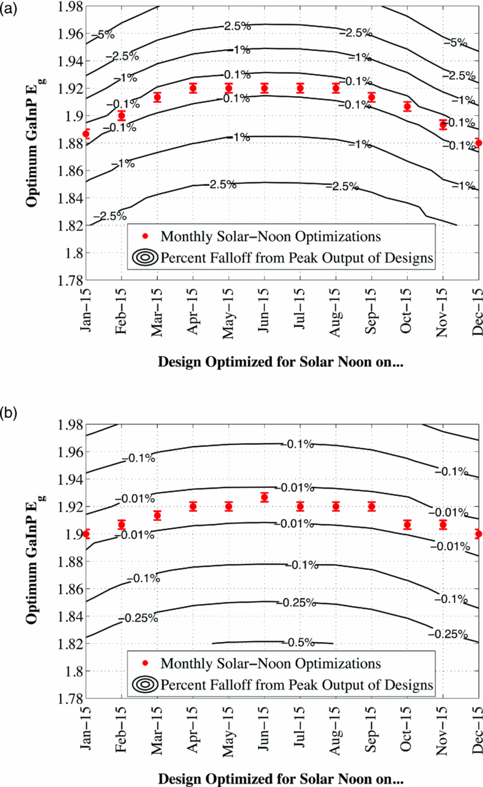 Faine2 showed that higher bandgap cells are more affected by changes in air mass because these changes primarily reduce the relative spectral energy in the low wavelength portion of the spectrum. Thus, the current-matching constraint in the two-terminal configuration causes it to be sensitive to spectral changes, as shown by the contours in Fig. 11. As was discussed earlier, for all designs the optimal GaAs base thickness was ≈4.6 to 4.7 μm and the optimal GaInP thickness ≈1.7 to 2.6 μm. However, these values are sensitive to the assumed recombination lifetimes/parameters and absorption coefficients and could thus vary significantly. 4.2.Daily and Monthly Energy DeliveryEach of the 13 optimized designs were simulated over the course of the day, 2 days per month (the 1st and 15th), in 10 min increments. The total daily, monthly, or yearly energy output of each design is calculated by assuming constant energy output throughout each 10 min increment and also throughout each 2 week interval. A comparison of the daily power output of the June 15th and December 15th designs, operating on both June 15th and December 15th, is shown in Fig. 12. Fig. 12Comparison of June 15th and December 15th designs, simulated over the course of the day on June 15th and December 15th in two- and three-terminal configurations. The three-terminal designs perform nearly identically and thus overlap. (a) Two-terminal configuration, (b) three-terminal configuration. 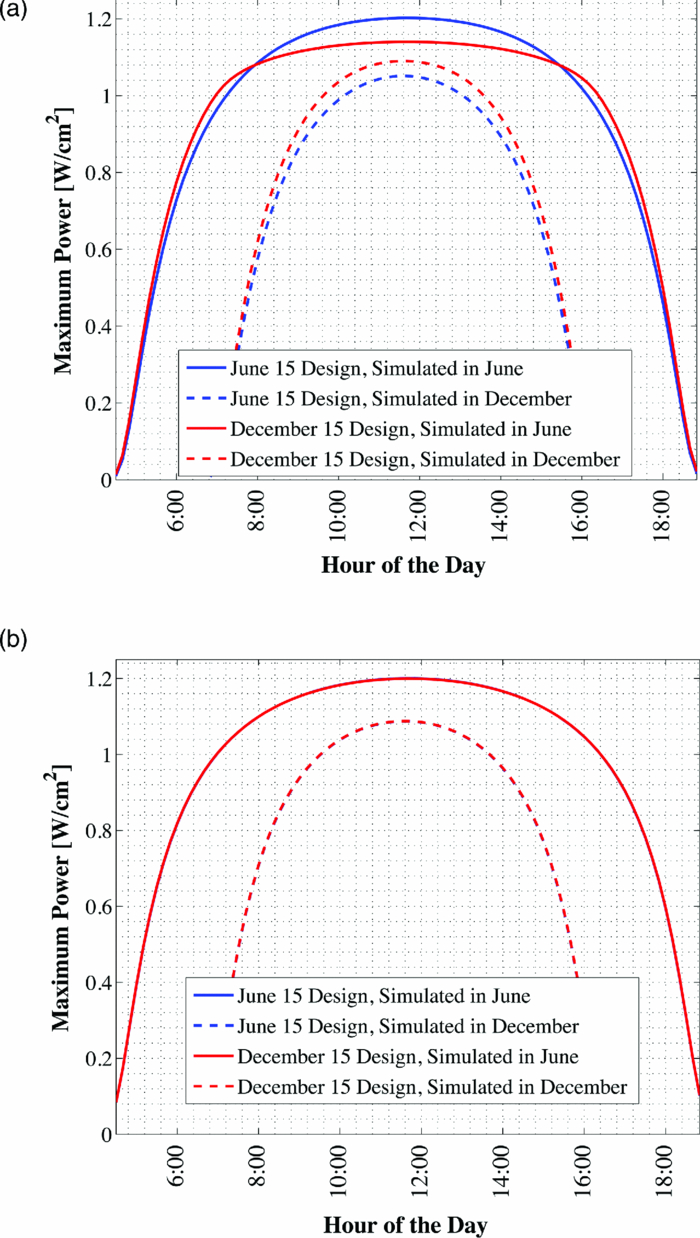 The three-terminal responses of the June 15th and December 15th designs shown in Fig. 12 are nearly the same because the optimal designs in these cases are essentially identical and very insensitive to even relatively large changes in GaInP bandgap [see Fig. 11]. However, the two-terminal configuration is much more sensitive to the specifics of the cell design [see Fig. 11]. While each design outperforms the other when operating at solar-noon in the month that it has been optimized for, the December design is always better in the morning and evening, even in June. This can be understood with the help of Fig. 13, which shows the normalized irradiance at solar-noon on June 15th and December 15th, in addition to the morning irradiance on June 15th. Due to an increased air mass, the energy in the high wavelength portion of morning spectra in June is reduced. Spectra throughout the day, even at solar-noon, in December are similarly affected by an increased air mass. Thus, while designing for high air mass does not produce peak output at solar-noon during the high-irradiance, low air mass summer months, it does allow for greater energy production in the morning and evening during these months when the air mass is increased relative to solar noon. Consequentially, one may expect that designing for high air mass, or some average air mass, should generate maximum yearly energy. Figure 14 shows the daily and monthly energy output for each optimal design (shown along the y-axis), normalized by the design of maximum output on each simulated day (shown along the x-axis). The three-terminal case is not shown, as the relative difference in daily energy output between any two optimized designs is less than 0.2%. Fig. 14Daily energy output for all designs for each simulated day of operation over the course of the year, normalized by the maximum value of all designs obtained for each day of operation. Looking across the plot for a particular design shows how the daily energy output of each changes over the course of the year. Looking down columns shows which design produces maximum energy on that day of operation. 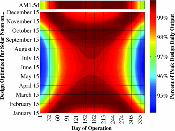 The relative sensitivity of the two-terminal configuration is reflected in Fig. 14, as the energy output of the two-terminal configuration may be as much as 5% below the maximum on any particular day. Additionally, Fig. 14 shows that a cell designed for peak power output at solar-noon in April through August will not generate maximum energy on any day of the year under ideal spectral conditions. Rather, maximum daily or monthly energy in both the two- and three-terminal configurations is generally achieved using spectra from early spring, late fall, or the AM1.5d standard. 4.3.Yearly Energy DeliveryThe total yearly energy output of each design is computed by assuming constant energy output within each 2 week interval. A smaller time step could have been used to improve the resolution of the total yearly energy output of each design; however, the results shown here constitute over 105 computer simulations; the slight potential improvement in the results achieved by increasing this number does not justify the added computation time required to run these simulations. The simulated yearly energy output of all the optimal monthly designs is shown in Fig. 15. Fig. 15Yearly energy output of all optimal designs for Las Vegas, Nevada shown zoomed in near the peaks. The energy harvesting efficiency, defined as the total yearly energy output divided by the total available yearly energy (3522 kW/h/m2 in Las Vegas), is given along the right-hand y-axis. 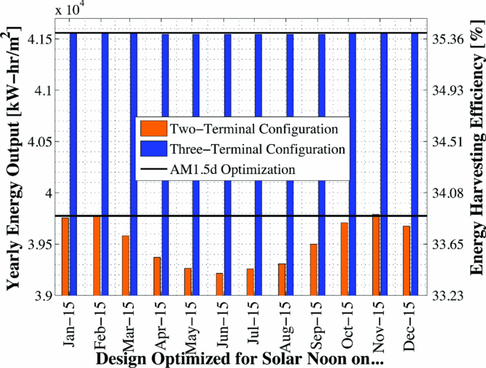 The three-terminal response is very insensitive to the month for which it has been designed; the difference in yearly energy output of the best and worst case three-terminal designs is less than 0.05% of the peak. On the other hand, a two-terminal design that is optimized for a November 15th solar-noon spectrum provides maximum yearly energy output, as the November 15th spectra provides a good weighted average of the spectral energy over the course of the year. However, all two-terminal designs produce at least 98.5% of the peak two-terminal output. 5.DiscussionThe difference in yearly energy production between a tandem designed for the mid-November spectra and AM1.5d is well within the accuracy of the optimization methodology and the assumptions of the detailed numerical models. It is preferable to design for AM1.5d in this case as one would achieve maximum yearly energy output while retaining the comparability to other laboratories provided by AM1.5d. However, these results could depend on geographic location, as Las Vegas has very low air mass throughout the year compared to other locations and AM1.5d is well matched to this condition. 5.1.Effect of Geographic LocationTo understand the role of geographic location, the simulations were repeated for two other locations with different degrees of relative air mass: Fraunhofer ISE, Germany, which has much greater relative air mass than Las Vegas, and Honolulu, Hawaii, which has much less relative air mass than Las Vegas (based upon the latitude). The two-terminal yearly energy production of the optimal monthly designs in these locations is shown in Fig. 16. The three-terminal configuration showed the same degree of insensitivity found for Las Vegas, Nevada, and has thus been omitted. Fig. 16Two-terminal yearly energy production of GaInP/GaAs tandems designed for operation in Germany and Hawaii. 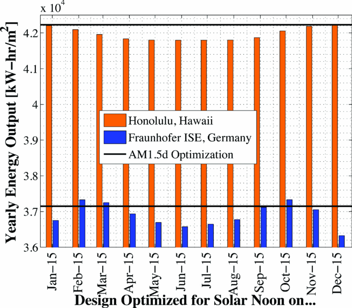 Figure 16 shows that location (or latitude) does play a role in determining the spectra that should be used during the design process to achieve maximum yearly energy production. In particular, as the relative air mass increases (latitude increases, in this case) an AM1.5d-based design becomes less ideal, though this difference is again only slight. The optimal design parameters for the three locations simulated in this work, and for the AM1.5d spectrum, are given in Table 3. Table 3Two- and three-terminal tandem design parameters optimized for maximum yearly energy output under spectra for Honolulu, Hawaii, Las Vegas, Nevada, Fraunhofer ISE, Germany, and the AM1.5d standard spectrum.
While the design parameters shown in Table 3 may indicate that a separate tandem design is required for each geographical installation location, optimizing for the AM1.5d spectrum produced essentially peak yearly energy in all locations. Thus, one would expect to achieve nearly maximum energy production for a tandem installed in a wide range of geographical locations if it has been optimized for this standard spectrum. Nevertheless, the small energy gain achieved by optimizing for a location-specific spectrum may be justified in some cases, especially for very large installations. 5.2.Effect of Optical ConcentrationIn addition to the assumed optical concentration of 33 suns used in the bulk of this work, results were also achieved for optical concentrations of 1, 250, and 500 suns. The optimal GaInP bandgap in the two-terminal configuration showed only a low degree of sensitivity to optical concentration. Figure 17 shows the yearly energy output (per unit concentration) for each of these designs. The three-terminal configuration is not shown as the results exhibit the same degree of insensitivity to the design spectrum shown earlier. Fig. 17Yearly energy production per sun optical concentration for all optimized monthly designs at various optical concentrations in the two-terminal configuration. 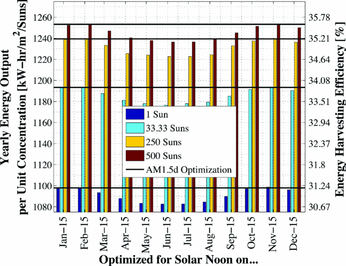 Though the optimal tandem design varies somewhat with optical concentration, the general trend, suggesting that an AM1.5d based design produces maximum yearly energy, is common among the designs at all optical concentrations. These results could depend upon the injection condition of the sub-cells under concentration; however, in all cases shown here, the quasineutral regions of both sub-cells remained in low-level injection. Series resistance plays an important role in device performance at high concentration; however, it would have a similar effect on each of the optimal designs for a particular concentration and thus would not significantly change the general trends shown here. 5.3.Comparison to Simple ModelIn order to justify the complexity of the detailed numerical models used in this work, it is a good exercise to compare the results to those that are achieved using simpler, more traditional models. This can be achieved by employing an ideal-diode model for both the GaInP and GaAs sub-cells, with the model parameters given in Table 4, where the dark-current density, J0, has been defined using two different methods: the Shockley–Queisser detailed-balance limit,11 as is common,12, 13 and by a semi-empirical state-of-the-art methodology, as proposed by Gray50 Table 4Ideal diode parameters for model comparison. The short-circuit current density was found by assuming an EQE of unity above the bandgap of each respective sub-cell. A junction temperature of 298.15 K was assumed in all cases.
Figure 18 shows a comparison of the optimal GaInP bandgap determined using ADEPT models and the simple ideal-diode model with dark-current found from detailed-balance and state-of-the-art assumptions. Fig. 18Comparison of optimal GaInP sub-cell bandgap in two- and three-terminal con- figurations calculated using ADEPT and an ideal-diode model with dark-current density, J0, determined using detailed-balance and a “state-of-the-art” approximation. (a) Two-terminal configuration, (b) three-terminal configuration. 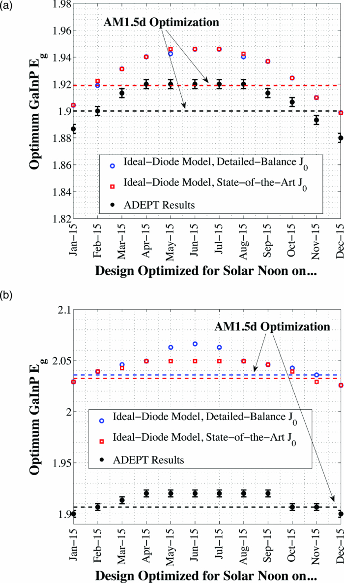 The most significant factor in the difference in bandgap between the ideal-diode and ADEPT models is the assumption in the simple case that the EQE is unity for both sub-cells above their respective bandgaps. This assumption does not hold for real cells due to absorption, and subsequent recombination in the near front-surface layers, which tends to drive the IQE (and thus the EQE) down at high photon energies (see Fig. 7). The result of this EQE = 1 assumption is that additional current is generated in both sub-cells, particularly in the GaInP sub-cell. This increases the optimal GaInP bandgap. In the two-terminal case, this increase is relatively small because the sub-cells must still be current matched. However, the increase in the three-terminal case is much more significant. The yearly energy generated by a GaInP/GaAs tandem in both two- and three-terminal configurations was calculated using the ideal-diode model with the optimal GaInP bandgaps shown in Fig. 18. The results of this calculation for the two-terminal configuration are shown in Fig. 19. Fig. 19Two-terminal yearly energy output calculated using an ideal-diode model for GaInP/GaAs tandem cells with the optimal GaInP bandgaps given in Fig. 18. 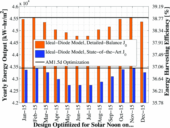 Figures 18, 19 show that while the optimal GaInP sub-cell bandgaps predicted by the ideal-diode models are somewhat different than those predicted by the realistic ADEPT model, the trends in total yearly energy delivery are nearly identical: essentially maximum energy is produced for a tandem designed for AM1.5d. Nevertheless, the ideal-diode–based model is not as useful of a tool for design because it cannot provide the optimal sub-cell base layer thicknesses. A more complicated formulation of the simple model14, 15 may be used for this purpose, but again, even these formulations make several simplifying assumptions about carrier recombination and material quality16 that are not assumed in the detailed model. 6.ConclusionsA GaInP/GaAs tandem solar cell was designed for daily, monthly, and yearly energy delivery using detailed numerical models by optimizing the GaInP bandgap and GaInP and GaAs sub-cell absorber layer thicknesses. Though modern multijunction concentrator solar cells typically employ three or more junctions, dual junction tandems are still relevant for use in spectrally split systems. Designing for a less than ideal spectrum will result in a daily or monthly energy production loss of, at most, 5% of the peak value in the two-terminal case, and 0.2% of the peak value in the three-terminal case. Similarly, designing for a less than optimal spectrum will produce within 1.5% of the peak yearly energy output. However, optimizing for the AM1.5d standard spectrum produces essentially peak energy for geographic locations between 21.3° (Honolulu, HI) and 48.1° (Fraunhofer, ISE, Germany) latitude. This result is independent of the optical concentration up to at least 500 suns, though the operating concentration does have some effect on the optimal tandem design parameters. A simple diode model with idealized assumptions generally predicts higher optimal GaInP bandgaps than the detailed models. If an ideal-diode model is employed in the design of a three-terminal tandem, the assumption that the EQE is unity above the GaInP bandgap should not be employed, as this was the primary source of this significant error. The effects of junction temperature (as was considered by Kinsey51), weather, and surface reflectance were not included in this analysis, nor were any joule losses. These effects, and others, may have some influence on the optimal tandem design and subsequent energy output. Additionally, the optimization scheme did not consider all design factors that may affect device performance, such as layer doping or window layer design. AcknowledgmentsWe would like to thank Allen Gray and Emcore Corporation for providing the details of the GaInP/GaAs tandem structure and the measured EQE used in this work for model verification. This work was supported by DuPont through the Very High Efficiency Solar Cell (VHESC) program funded by the Defense Advanced Research Projects Agency (DARPA), Contract No. HR0011-07- 9-0005. The views, opinions, and/or findings contained in this article are those of the author and should not be interpreted as representing the official views or policies, either expressed or implied, of the Defense Advanced Research Projects Agency or the Department of Defense. This document has been approved for public release, distribution unlimited. ReferencesStandard tables for reference solar spectral irradiances: Direct normal and hemispherical on 37 degree tilted surface,”
(2003) Google Scholar
P. Faine, S. R. Kurtz, C. Riordan, and J. Olson,
“The influence of spectral solar irradiance variations on the performance of selected single-junction and multijunction solar cells,”
Sol. Cells, 31
(3), 259
–278
(1991). http://dx.doi.org/10.1016/0379-6787(91)90027-M Google Scholar
A. Berk, L. S. Bernstein, and D. C. Robertson,
“MODTRAN: A moderate resolution model for LOWTRAN7,”
(April 1989). Google Scholar
A. Berk, G. P. Anderson, P. K. Acharya, L. S. Bernstein, L. Muratov, J. Lee, M. J. Fox, S. M. Adler-Golden, J. H. Chetwynd Jr., M. L. Hoke, R. B. Lockwood, J. A. Gardner, T. W. Cooley, and P. E. Lewis,
“MODTRAN5: A reformulated atmospheric band model with auxiliary species and practical multiple scattering options,”
341
–347
(2004). Google Scholar
G. S. Kinsey and K. M. Edmondson,
“Spectral response and energy output of concentrator multi-junction solar cells,”
Prog. Photovoltaics, 17
(5), 279
–288
(2008). http://dx.doi.org/10.1002/pip.875 Google Scholar
A. W. Haas, J. R. Wilcox, J. L. Gray, and R. J. Schwartz,
“Design of 2- and 3-terminal GaInP/GaAs concentrator cells for maximum yearly energy output,”
(2010). Google Scholar
M. A. Green, K. Emery, Y. Hishikawa, and W. Warta,
“Solar cell efficiency tables (version 36),”
Prog. Photovoltaics, 18 346
–352
(2010). http://dx.doi.org/10.1002/pip.1021 Google Scholar
A. Barnett, D. Kirkpatrick, C. Honsberg, D. Moore, M. Wanlass, K. Emery, R. Schwartz, D. Carlson, S. Bowden, D. Aiken, A. Gray, S. Kurtz, L. Kazmerski, M. Stiener, J. Gray, T. Davenport, R. Buelow, L. Takacs, N. Shatz, J. Bortz, O. Jani, K. Goosen, F. Klamilev, A. Doolittle, I. Ferguson, B. Unger, G. Schmidt, E. Christensen, and D. Salzman,
“Very high efficiency solar cell modules,”
Prog. Photovoltaics, 17
(1), 75
–83
(2009). http://dx.doi.org/10.1002/pip.852 Google Scholar
J. D. McCambridge, M. A. Steiner, B. L. Unger, K. A. Emery, E. L. Christensen, M. W. Wanlass, A. L. Gray, L. Takacs, R. Buelow, T. A. McCollum, J. W. Ashmead, G. R. Schmidt, A. W. Haas, J. R. Wilcox, J. V. Meter, J. L. Gray, D. T. Moore, A. M. Barnett, and R. J. Schwartz,
“Compact spectrum splitting photovoltaic module with high efficiency,”
Prog. Photovoltaics, 19
(3), 352
–360
(2011). http://dx.doi.org/10.1002/pip.1030 Google Scholar
M. A. Green and A. Ho-Baillie,
“Fourty three per cent composite split spectrum concentrator solar cell efficiency,”
Prog. Photovoltaics, 18 42
–47
(2010). http://dx.doi.org/10.1002/pip.924 Google Scholar
W. Shockley and H. J. Queisser,
“Detailed balance limit of efficiency of p-n junction solar cells,”
J. Appl. Phys., 32
(3), 510
–519
(1961). http://dx.doi.org/10.1063/1.1736034 Google Scholar
S. P. Philipps, G. Peharz, T. Hornung, R. Hoheisel, N. M. Al-Abbadi, F. Dimroth, and A. W. Bett,
“A theoretical analysis on the energy production of III-V multi-junction solar cells under realistic spectral conditions,”
121
–125
(2009). Google Scholar
G. Letay, C. Baur, and A. W. Bett,
“Theoretical investigations of III-V multi- junction concentrator cells under realistic spectral conditions,”
(2004). Google Scholar
H. J. Hovel,
“Solar Cells,”
Semiconductors and Semimetals, 2 Academic Press, New York
(1976). Google Scholar
A. L. Fahrenbruch and R. H. Bube, Fundamentals of Solar Cells: Photovoltaic Solar Energy Conversion, Academic Press, New York
(1983). Google Scholar
S. R. Kurtz, J. M. Olson, K. Bertness, D. J. Friedman, J. F. Geisz, and A. E. Kibbler,
“Passivation of interfaces in high-efficiency photovoltaic devices,”
95
–106
(1999). Google Scholar
A. L. Gray, M. Stan, T. Varghese, A. Korostyshevsky, J. Doman, A. Sandoval, J. Hills, C. Griego, M. Turner, P. Sharps, A. Haas, J. Wilcox, J. Gray, and R. Schwartz,
“Multi-terminal dual junction InGaP2/GaAs solar cells for hybrid system,”
1
–4
(2008). Google Scholar
J. Gray,
“Adept: a general purpose numerical device simulator for modeling solar cells in one-, two-, and three-dimensions,”
436
–438
(1991). Google Scholar
R. King, C. Fetzer, P. Colter, K. Edmondson, J. Ermer, H. Cotal, H. Yoon, A. Stavrides, G. Kinsey, D. Krut, and N. Karam,
“High-efficiency space and terrestrial multijunction solar cells through bandgap control in cell structures,”
776
–781
(2002). Google Scholar
M. A. Steiner, L. Bhusal, J. F. Geisz, A. G. Norman, M. J. Romero, W. J. Olavarria, Y. Zhang, and A. Mascarenhas,
“CuPt ordering in high bandgap Ga(x)In(1−x)P alloys on relaxed GaAsP step grades,”
J. Appl. Phys., 106
(6), 063525
(2009). http://dx.doi.org/10.1063/1.3213376 Google Scholar
S. R. Kurtz, J. M. Olson, and A. Kibbler,
“Effect of growth rate on the band gap of Ga0.5In0.5P,”
Appl. Phys. Lett., 57
(18), 1922
–1924
(1990). http://dx.doi.org/10.1063/1.104013 Google Scholar
C. Alibert, G. Bordure, A. Laugier, and J. Chevallier,
“Electroreflectance and band structure of Ga(x)InP(1−x) alloys,”
Phys. Rev. B, 6
(4), 1301
–1310
(1972). http://dx.doi.org/10.1103/PhysRevB.6.1301 Google Scholar
J. F. Geisz, S. Kurtz, M. W. Wanlass, J. S. Ward, A. Duda, D. J. Friedman, J. M. Olson, W. E. McMahon, T. E. Moriarty, and J. T. Kiehl,
“High-efficiency GaInP/GaAs/InGaAs triple-junction solar cells grown inverted with a metamorphic bottom junction,”
Appl. Phys. Lett., 91 023502
(2007). http://dx.doi.org/10.1063/1.2753729 Google Scholar
T. Takamoto, E. Ikeda, and H. Kurita,
“Over 30% efficient InGaP/GaAs tandem solar cells,”
Appl. Phys. Lett., 70
(3), 381
–383
(1997). http://dx.doi.org/10.1063/1.118419 Google Scholar
M.-J. Yang, M. Yamaguchi, T. Takamoto, E. Ikeda, H. Kurita, and M. Ohmori,
“Photoluminescence analysis of InGaP top cells for high-efficiency multi- junction solar cells,”
Sol. Energy Mater. Sol. Cells, 45
(4), 331
–339
(1997). http://dx.doi.org/10.1016/S0927-0248(96)00079-7 Google Scholar
K. A. Bertness, S. R. Kurtz, D. J. Friedman, and A. E. Kibbler,
“29.5%-efficient GaInP/GaAs tandem solar cell,”
Appl. Phys. Lett., 65 989
–991
(1994). http://dx.doi.org/10.1063/1.112171 Google Scholar
T. Shitara and K. Eberl,
“Electronic properties of InGaP grown by solid-source molecular-beam epitaxy with a gap decomposition source,”
Appl. Phys. Lett., 65
(3), 356
–358
(1994). http://dx.doi.org/10.1063/1.112373 Google Scholar
Y. A. Goldberg, Handbook Series on Semiconductor Parameters, 1 104
–121 World Scientific, London
(1996). Google Scholar
N. Shmidt, Handbook Series on Semiconductor Parameters, 1 169
–190 World Scientific, London
(1996). Google Scholar
A. Dargys and J. Kundrotas, Handbook on Physical Properties of Ge, Si, GaAs and InP, Science and Encyclopedia Publishers(1994). Google Scholar
G. Schmiedel, P. Kiesel, G. H. Dohler, E. Greger, K. H. Gulden, H. P. Schweizer, and M. Moser,
“Electroabsorption in ordered and disordered GaInP,”
J. Appl. Phys., 81
(2), 1008
–1010
(1997). http://dx.doi.org/10.1063/1.364195 Google Scholar
Y. A. Goldberg, Handbook Series on Semiconductor Parameters, 2 37
–61 World Scientific, London
(1999). Google Scholar
P. T. Landsberg, Recombination in Semiconductors, Cambridge University Press, Cambridge
(1991). Google Scholar
T. Takamoto, E. Ikeda, H. Kurita, and M. Ohmori,
“Structural optimization for single junction InGaP solar cells,”
Sol. Energy Mater. Sol. Cells, 35 25
–31
(1994). http://dx.doi.org/10.1016/0927-0248(94)90118-X Google Scholar
T. Kato, T. Matsumoto, and T. Ishida,
“Electrical properties of Zn-doped In(1−x)Ga(x)P,”
Jpn. J. Appl. Phys., 19
(12), 2367
–2375
(1980). http://dx.doi.org/10.1143/JJAP.19.2367 Google Scholar
M.-J. Yang, M. Yamaguchi, T. Takamoto, E. Ikeda, H. Kurita, and M. Ohmori,
“Photoluminescence analysis of InGaP top cells for high-efficiency multi-junction solar cells,”
Sol. Energy Mater. Sol. Cells, 45
(4), 331
–339
(1997). http://dx.doi.org/10.1016/S0927-0248(96)00079-7 Google Scholar
J. L. Gray, Handbook of Photovoltaic Science and Engineering, 62
–112 1st Ed.Wiley, West Sussex, England
(2003). Google Scholar
J. L. Gray,
“Two-dimensional modeling of silicon solar cells,”
Purdue University,
(1982). Google Scholar
G. B. Lush, H. F. MacMillan, B. M. Keyes, D. H. Levi, M. R. Melloch, R. K. Ahrenkiel, and M. S. Lundstrom,
“A study of minority carrier lifetime versus doping concentration in n-type GaAs grown by metalorganic chemical vapor deposition,”
J. Appl. Phys., 72
(4), 1436
–1442
(1992). http://dx.doi.org/10.1063/1.351704 Google Scholar
H. C. Casey, D. D. Sell, and K. W. Wecht,
“Concentration dependence of the absorption coefficient for n- and p-type GaAs between 1.3 and 1.6 eV,”
J. Appl. Phys., 46
(1), 250
–257
(1974). http://dx.doi.org/10.1063/1.321330 Google Scholar
M. E. Levinshtein and S. L. Rumyantsev, Handbook Series on Semiconductor Parameters, 1 77
–103 World Scientific, London
(1996). Google Scholar
D. L. Rode, Semiconductors and Semimetals, 10 91 Academic Press, New York
(1975). Google Scholar
D. L. Rode, Semiconductors and Semimetals, 10 1 Academic Press, New York
(1975). Google Scholar
V. P. Varshni,
“Band-to-Band Radiative Recombination in Groups IV, VI, and III-V Semiconductors (I),”
Phys. Status Solidi, 19
(2), 459
–514
(1967). http://dx.doi.org/10.1002/pssb.19670190202 Google Scholar
V. P. Varshni,
“Band-to-Band Radiative Recombination in Groups IV, VI, and III–V Semiconductors (II),”
Phys. Status Solidi, 20
(1), 9
–36
(1967). http://dx.doi.org/10.1002/pssb.19670200102 Google Scholar
A. L. Gray,
“EQE data from RE879,”
(2008) Google Scholar
M. C. DeLong, D. J. Mowbray, R. A. Hogg, M. S. Skolnick, J. E. Williams, K. Meehan, S. R. Kurtz, J. . Olson, R. P. Schneider, M. C. Wu, and M. Hopkinson,
“Band gap of “completely disordered” Ga(0.52)In(0.48)P,”
Appl. Phys. Lett., 66
(23), 3185
–3187
(1995). http://dx.doi.org/10.1063/1.113717 Google Scholar
J. M. Olson, S. R. Kurtz, A. E. Kibbler, and P. Faine,
“A 27.3% efficient Ga(0.5)In(0.5)P/GaAs tandem solar cell,”
Appl. Phys. Lett., 56
(7), 623
–625
(1990). http://dx.doi.org/10.1063/1.102717 Google Scholar
D. Friedman, S. Kurtz, K. Bertness, A. Kibbler, C. Kramer, J. Olson, D. King, B. Hansen, and J. Snyder,
“GaInP/GaAs monolithic tandem concentrator cells,”
1829
–1832
(1994). Google Scholar
J. L. Gray, J. M. Schwarz, J. R. Wilcox, A. W. Haas, and R. J. Schwartz,
“Peak efficiency of multijunction photovoltaic systems,”
(2010). Google Scholar
G. S. Kinsey, P. Herbert, K. E. Barbour, D. D. Krut, H. L. Cotal, and R. A. Sherif,
“Concentrator multijunction solar cell characteristics under variable intensity and temperature,”
Prog. Photovoltaics, 16 503
–508
(2008). http://dx.doi.org/10.1002/pip.834 Google Scholar
|
|||||||||||||||||||||||||||||||||||||||||||||||||||||||||||||||||||||||||||||||||||||||||||||||||||||||||||||||||||||||||||||||||||||||||||||