|
|
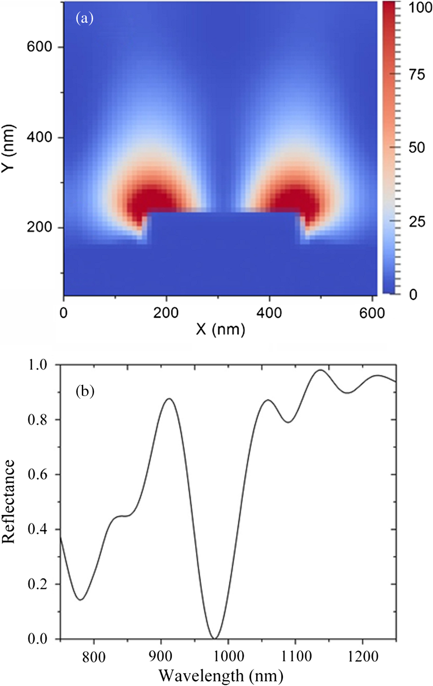
1.IntroductionSilicon (c-Si) is the most common material used in solar cells. 1 , 2 However, the energy produced from c-Si solar cells is expensive due to the high cost of ultrapure crystalline silicon and its medium power conversion efficiency. Thin-film solar cells may provide more cost-effective photovoltaics in the long term due to the thin absorber layer and less stringent requirements in the purity and crystallinity of the absorber. However, thin-film inorganic solar cells based on amorphous Si, 3 cadmium telluride, 4 , 5 and copper indium gallium selenide, 6 and organic solar cells based on small-molecule organic dyes 7 , 8 and polymers 9 all exhibit a large absorption loss in the infrared spectrum as the absorption coefficient of the absorber layer vanishes beyond 800 to 900 nm. Figure 1(a) shows the loss in the number of photons (red line) and energy of sub-bandgap photons (black line) in the AM1.5 spectrum as a function of bandgap of the photovoltaic material and its associated cut-off wavelength. The photon loss is normalized to the total number of photons in AM1.5 spectrum and energy loss is normalized to the total energy of light in AM1.5 spectrum ( ). Fig. 1(a) Loss in the number and energy of AM1.5 solar spectrum as a function of the bandgap of common photovoltaic materials and their associated cut-off wavelength. (b) Schematic of an upconversion-based thin-film solar cell in a superstrate architecture. (c) Schematic of an upconversion-based thin-film solar cell in a substrate architecture. 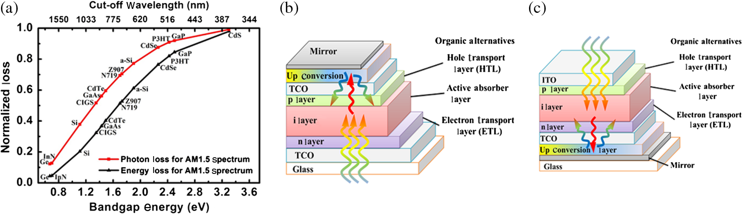 Upconversion of low-energy photons into high-energy photons can reduce these absorption losses and widen the absorption window of solar cells. Trupke et al. suggest that the theoretical upper limit for the efficiency of a silicon solar cell can be enhanced from 30 to 47.6% by upconversion of low-energy photons into photons within the absorption band of the solar cell, 10 assuming complete recovery of sub-bandgap photons. Figure 1(b) and 1(c) illustrates the possible integration of an upconversion layer into the structure of conventional inorganic or organic thin-film solar cells. However, utilizing upconversion concepts in solar cells has been very challenging, mainly due to (1) the very low efficiency of the upconversion process under AM1.5 illumination conditions (low-power regime), (2) the narrowband nature of upconversion in current upconversion materials, and (3) the small absorption coefficient of upconversion materials. This article tackles the first and the third challenges by enhancing the interaction of incident light with the upconversion nanomaterials through plasmonic field enhancement. A major challenge of upconversion-based solar cells is to find efficient upconversion materials. Sodium yttrium fluoride ( ) nanoparticles doped with erbium (Er) as the emitter and ytterbium (Yb) as the sensitizer is one of the most efficient upconversion materials reported to date. 11 ions absorb near-infrared (NIR) light at 980 nm and sequential energy-transfer events from Yb to Er excites visible Er emission at 665 and 540 nm. The intensity of two-photon upconversion luminescence in this material system is proportional to the square of the incident light intensity. As a result, the efficiency of upconversion can be enhanced by concentrating sunlight into the upconversion material. Alternatively, the evanescent field in metallic nanostructures, produced by plasmon resonance with the excitation light, can lead to formation of electromagnetic hot spots at the metal/dielectric interface. 12 – 14 This property of plasmon resonance can be utilized to enhance the efficiency of two-photon upconversion. Plasmonic nanostructures have been explored extensively to improve the effective optical path length and absorption of incident photons in the absorber layer of inorganic and organic solar cells. 15 – 20 For our purposes, tuning the wavelength of the plasmon resonance to that of the absorption spectrum of the upconversion material is of great importance. Several approaches have been used for tuning the wavelength of the surface plasmon resonance, including engineering the size of metallic nanoparticles, 21 varying the thicknesses of double metallic layers, 22 and varying the periodicity in two-dimensional (2-D) lattices. 23 Also, colloidal noble-metal surfaces have been used to influence the optical properties (e.g., quantum efficiency, absorbance, polarization, directional emission, excited-state lifetime) of a wide variety of luminescent materials. 24 – 30 Metal nanostructures can influence the optical properties of a nearby emitter through (1) amplification of the excitation field in the vicinity of the metal surface, (2) modification of the intrinsic radiative and nonradiative transition rates of the phosphor, and (3) controlling emission directionality. 24 , 25 , 29 The emission rate, , for a simple system far from saturation is given by where is the excitation rate, is the radiative rate, and is the nonradiative rate. The first effect, amplification of the excitation electric field, , increases the emission rate by increasing the excitation rate, , according to , where is the transition dipole moment. The second effect works through modification of the intrinsic radiative and nonradiative processes of the phosphor via near-field interaction with the metal surface, thereby changing and . Luminescence is enhanced (i.e., is increased) if energy transfer from the emitter to the metal structure is re-emitted as radiation to the far field. Emission is quenched (i.e., is increased) if the energy transferred to the metal is damped within the metal structure and lost as heat. As a brief review of the prior art, Song et al. 31 in 2005 reported a enhancement of emission from CdSe/ZnS quantum dots in the presence of surface plasmons. Surface plasmons were excited on a surface consisting of Ag nanoparticles interconnected by an Ag film. Silva et al. 32 reported an upconversion enhancement in Er-doped PbO- glasses containing Ag nanoparticles with an average diameter of 2 nm. Aisaka et al. 33 reported a enhancement of upconversion photoluminescence from Er-doped films in the visible range and in the infrared range through plasmon resonance on Ag nanoparticles. In 2010, Schietinger et al. 34 reported plasmon-enhanced upconversion in single nanoparticles codoped with ions. We recently demonstrated the feasibility of using engineered plasmonic surfaces to enhance NIR-to-visible upconversion luminescence from nanocrystalline systems. 35 The major focus of that paper was the synthesis of nanoparticles and characterization of two-photon upconversion enhancement due to an engineered plasmonic surface. This approach is attractive because the use of engineered surfaces offers the possibility of much greater control over the location and distribution of local-field enhancement zones relative to plasmonic materials based on colloidal metal nanostructures.This article describes the process used to design a plasmonic upconversion enhancer using rigorous three-dimensional finite-difference time domain (3D-FDTD) simulations, followed by the fabrication and characterization of the enhancer. The focus of the paper is on quantifying the plasmon-assisted upconversion mechanism, assessing the loading effect of the absorptive upconversion layer on the field enhancement of the plasmonic crystal, and evaluating the viability of this approach for photovoltaic application through a rational experimental—modeling approach. It should be noted that solar cells require a wideband absorption spectrum; therefore, a wideband upconversion process is highly preferred. However, we have purposefully focused on upconversion of 980-nm photons through : 3% Er, 17% Yb, because the two-photon upconversion process in this material system is the most efficient upconversion process discovered to date. The methodology developed in this article to enhance upconversion efficiency through plasmonics can be expanded to wideband upconversion once new materials with efficient wideband upconversion properties are developed. 2.Design of Gold Nanopillars for Maximum Plasmon ActivitySurface plasmons are the electromagnetic surface modes coupled with free electrons in metallic surfaces. Plasmon activity in nanostructured metallic surfaces can be simulated by solving Maxwell’s equation via a 3D-FDTD approach, which discretizes the time-dependent Maxwell’s equations into space and time grids 36 without using any approximation. This simulation approach can be used to study the potential efficiency enhancement of upconverters by simulating the enhanced electric-field intensity. The theory of excitation of surface plasmons on the 2-D gold-nanopillar arrays, and the FDTD simulation procedures used, are described in our earlier publications. 12 – 14 Since plasmonic resonances result in the absorbance of incident light, maximum plasmonic activity can be associated with minimum light reflection. Therefore, in this work, reflection simulations and measurements are utilized to study plasmonic resonance and field enhancement in 2-D plasmonic crystals. The plasmonic crystal described in this study is composed of a square-lattice array of gold nanopillars on a continuous gold surface, coated with a film of poly(methylmethcrylate) (PMMA) with a refractive index of 1.49, as shown in Fig. 2. All the reflectance and field enhancements in this study are simulated at normal incident angle. Figure 3 shows the specular reflectance of 980-nm light as a function of lattice period ( in axis) and nanopillar diameter ( in axis) by the plasmonic crystals with a nanopillar height ( ) of 70 nm. (The maximum absorbance of the Yb sensitizers is at 980 nm.) The period of the nanopillars was varied from 500 to 800 nm, and the diameter of the nanopillars was varied from 200 to 500 nm. A sharp minimum reflectance is observed for a lattice constant of 620 nm and a nanopillar diameter of 310 nm. We expect the surface plasmons in this structure to be more selective than localized plasmons as they involve the interaction of light with the highly ordered periodic lattice (Bloch modes). This is because plasmon resonance in 2-D metallic plasmonic crystals originates from the interplay between both surface plasmon polaritons (SPP) and localized plasmons. Nevertheless, in certain geometrical regions, the SPPs may dominate the plasmonic activity, whereas, in other regimes, localized plasmons might be the limiting mechanism. Due to the long-range propagation of Bloch modes, SPP-limited plasmon resonance is much more sensitive to the period of the grating compared to the resonance due to localized plasmons. Therefore, the regions most sensitive to grating period appear to be SPP-limited, whereas regions that are relatively insensitive to the period of the grating should be localized-plasmon-limited. Fig. 2Top view of nanopillars in square lattice (a). Three-dimensional view of the unit cell of a plasmonic crystal composed of cylindrical nanopillars of diameter and spacing in a square lattice (b). 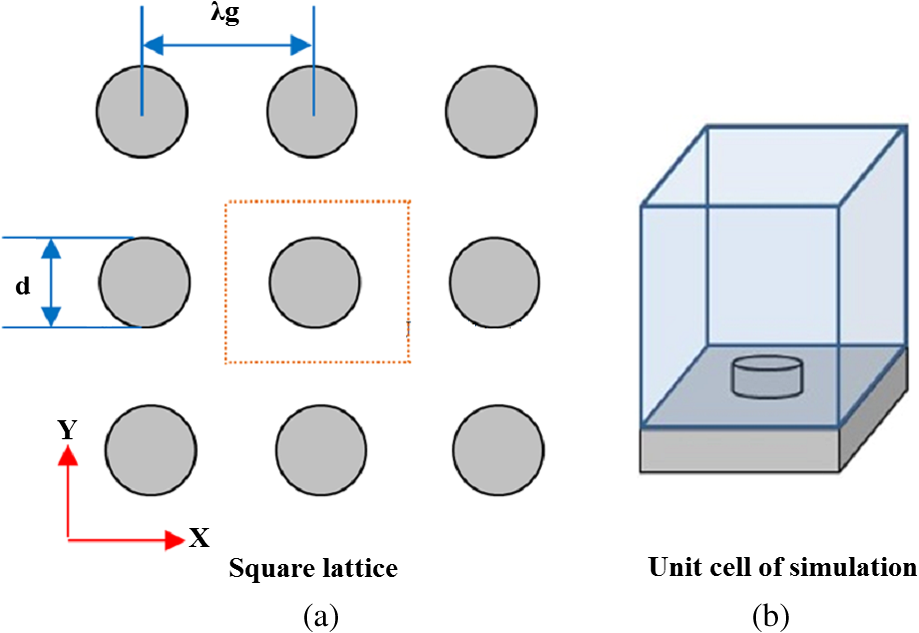 Fig. 3Specular reflectance of 980-nm incident light from plasmonic crystals with respect to the diameter and spacing of the cylindrical gold nanopillars in square lattice. The height of the nanopillars is 70 nm. 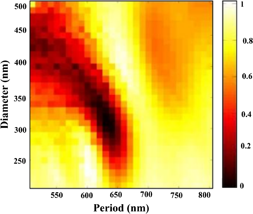 Therefore, the strong plasmonic activity around the lattice constant of 620 nm and nanopillar diameter of 310 nm can be attributed to surface plasmons, whereas the other reduced reflectance region, corresponding to the upper left segment of Fig. 3, is attributed to plasmon resonance localized on the nanopillars. Based on this study and our earlier study on the geometry dependence of plasmonic resonance in noble metal nanopillar arrays, 12 – 14 , 37 the optimum values for , , and were chosen to be 310, 620, and 70 nm, respectively. These design parameters should achieve the strongest plasmonic activity under 980-nm irradiation, and, hence, provide maximum excitation-rate enhancement for the Yb sensitizers. Figure 4(a) shows the spatial distribution of the electric-field intensity, normalized to that of the incident 980-nm light, in the plane of the unit cell at the cross-section of a gold nanopillar. A field enhancement of over is observed at the edge of the nanopillars, and a field enhancement greater than persists up to 300 nm throughout the majority of the volume above the top surface of nanopillars. Figure 4(b) shows the simulated reflectance spectrum of the optimized plasmonic crystal simulated at normal incident angle, confirming maximum plasmonic activity at 980 nm. 3.Fabrication and Measurement ProceduresElectron-beam lithography using a Hitachi SEM S-3400N, followed by a lift-off process, was used to make the square-lattice gold plasmonic crystal with a lattice constant of 620 nm, nanopillar diameter of 310 nm, and nanopillar height of 70 nm. The detailed process flow is as follows: glass substrates were cleaned using a standard RCA I cleaning procedure, followed by a 10 min hot wash. A 100-nm layer of gold was deposited on the glass substrates via a radio frequency sputtering method. A 300-nm-thick electron-beam resist, 495PMMA polymer, 6% solid in Anisole, was spin-coated onto the substrate at 4000 rpm for 45 s and prebaked for 1 min at 180°C. An electron-beam dose of was used to expose the sample using the square-lattice pattern designed using a Designcad pattern generator. Plasmonic crystals with dimensions were made at magnification. The exposed sample was developed in methylisobutylketone/isopropyl alcohol: solution for 25 s. A 70-nm-thick gold film was deposited above the patterned surface via an -beam evaporation method using a CHA (Fremont, California) electron-beam evaporator. The -beam resist was dissolved in PG Remover solution for 4 h and the gold layer above the resist was lifted off during this process. Each substrate included multiple plasmonic crystal regions, regions coated only with a planar gold film, and regions of bare glass. For upconversion enhancement studies, plasmonic substrates were spin-coated with a 105-nm thick film of PMMA impregnated with : 3% Er, 17% Yb nanoparticles. These nanocrystals were synthesized according to a previously published procedure. 11 The sol containing the upconversion nanocrystals consisted of 100 mg : 3% Er, 17% Yb nanoparticles and 100 mg PMMA in 10 mL of chloroform and 2 mL of toluene. Upconversion luminescence from the coated plasmonic substrate was measured using a scanning confocal microscope from Horiba Jobin Yvon with a 980-nm diode laser. The complete visible upconversion emission spectrum was acquired at each point of a 2-D grid scan over a selected area of the substrate. The scan areas were chosen to include both patterned and smooth-gold regions of the substrates, so the upconversion-luminescence intensity from the plasmonic crystal could be reliably compared to that from the planar gold. The reflection spectra from gold nanopillar regions and gold film region were measured using a Fourier transform infrared spectroscopy (FTIR) microscope at the National Renewable Energy Laboratory. The Continuum infrared microscope was coupled to an FTIR spectrometer (Nicolet 6700). A CaF beam splitter with white light illumination from a quartz-halogen source and an MCT (HgCdTe) detector were used to make measurements in a microreflectance mode with a 100 μm square aperture. Spectra were acquired from an average of a minimum of 128 scans with a system resolution of . 4.Experimental Results and AnalysisFigure 5(a) shows a SEM image of a plasmonic crystal fabricated as described above. The observed nanopillar spacing and diameter are in an excellent agreement with the targeted design parameters ( error in dimensions). The height of the nanopillars was measured with an atomic force microscope in contact mode. Figure 5(b) shows a line scan over a single row of nanopillars. The height was measured to be approximately 70 nm, and the lattice constant was measured as 615 nm (less than 1% difference from the designed dimension). These results demonstrate that the fabrication process provides remarkable accuracy in making designed plasmonic crystals. Fig. 5(a) SEM image of gold nanopillars on a gold surface over a 100-nm gold layer created from electron-beam lithography. (b) Topographic line scans over a row of gold nanopillars using AFM. 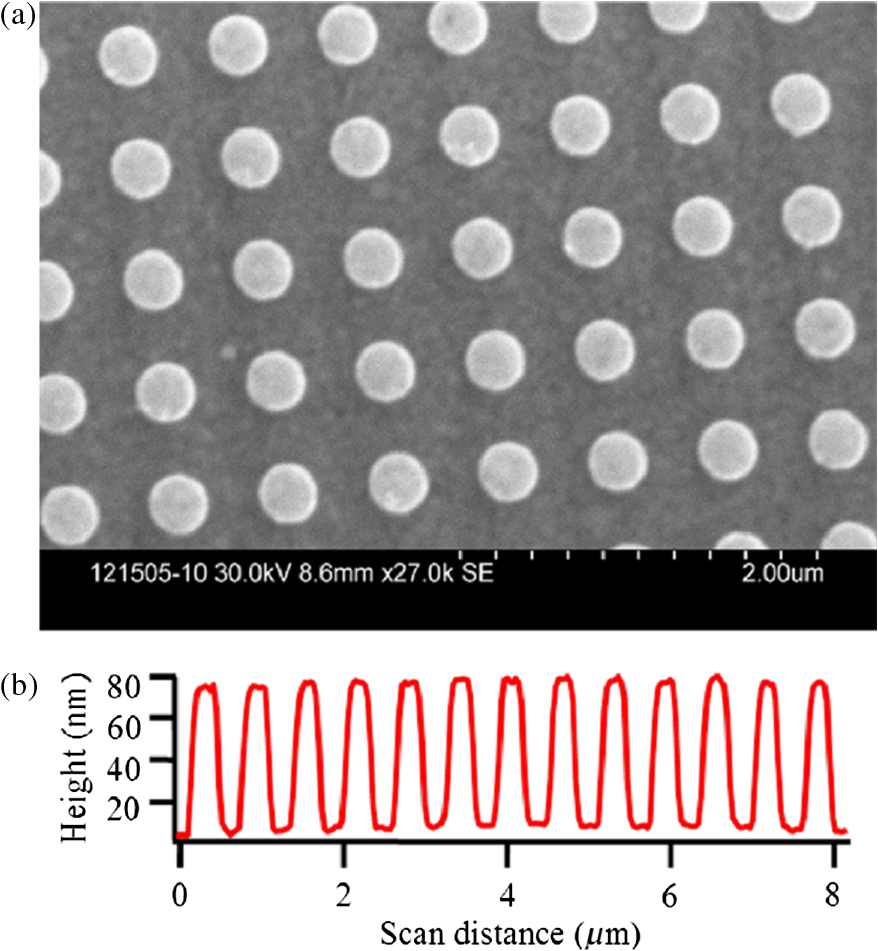 The measured reflectance spectrum of the plasmonic crystal coated with a 105-nm-thick upconversion film is shown in Fig. 6. For comparison, Fig. 6 also includes the reflectance spectrum of a smooth-gold segment of the substrate. (The increased noise at the short-wavelength end of the spectrum is a result of approaching the wavelength limit of the instrument response.) A plasmonic resonance is observed within the wavelength window of 950 to 1050 nm, with a reflection minimum at 998 nm. The minimum shows a 1.8% red-shift with respect to the target wavelength (980 nm). This red-shift is minimal, however, and significant reflectance is observed at 980 nm. Overall, excellent agreement is observed between the measured and anticipated resonance behavior of the fabricated plasmonic crystal, confirming the validity and effectiveness of our design and fabrication methodology. The ability to design surfaces with a desired plasmonic activity is a major advantage of plasmonic crystals over colloidal plasmonic nanoparticles. Fig. 6Reflectance spectra from the sample substrate coated with an upconversion layer. The red curve is the spectrum from an adjacent smooth surface, and the dotted blue curve is the spectrum from the patterned plasmonic surface. The increased noise at the short-wavelength end of the spectrum is a result of approaching the wavelength limit of the instrument response. 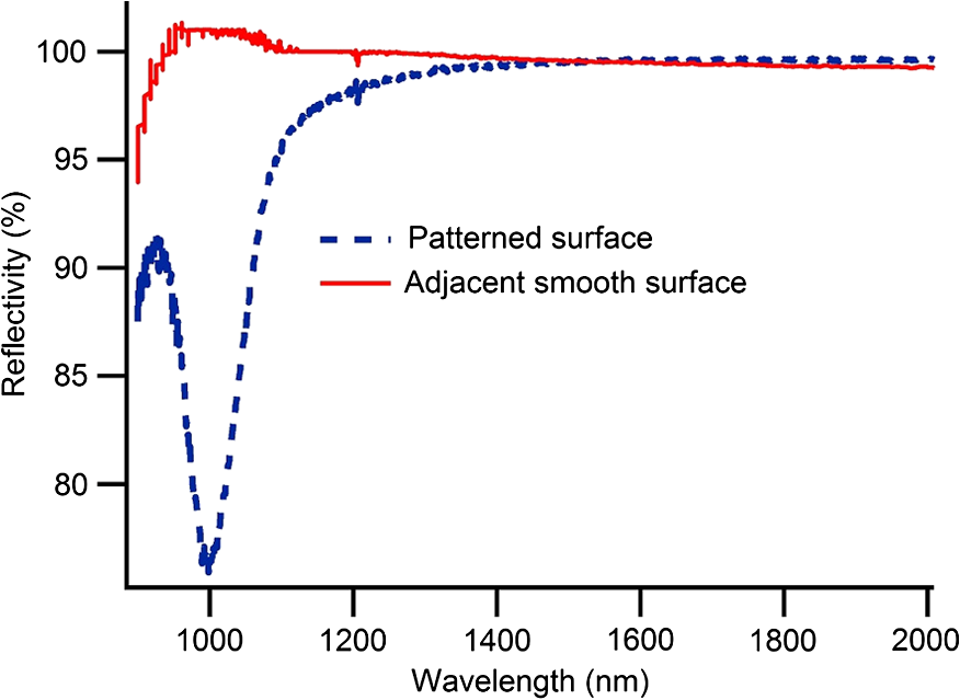 Figure 7(a) shows an optical image of a targeted scan area of the sample at a bare glass/planar gold interface. The red dots in Fig. 7(a) are the focusing marks for the optical image, and the green dot is due to upconversion emission, indicating the location of the scanning laser beam. Confocal upconversion images of the area in Fig. 7(a) showing the measured green (540 nm) and red (660 nm) emission intensities are shown in Fig. 7(b) and 7(c). On average, green emission from the smooth-gold region is brighter than that from the bare glass. The red emission is brighter. The major part of this upconversion enhancement is attributed to mirror effects, in which the gold layer reflects both excitation and emission light back into the upconversion layer, thereby increasing the effective excitation intensity as well as the fraction of collected emission. The larger enhancement of red relative to green in Fig. 7(b) and 7(c) is due to the increased reflectivity of gold at red relative to green. Plasmonic activity is not expected on the smooth-gold surface, as evidenced by the lack of structure in the reflectance spectrum (blue curve) in Fig. 6. Note that the reflectance for smooth gold at 980 nm is close to unity. Fig. 7(a) Optical image of a gold/glass substrate coated with an upconversion film ( : 3% Er, 17% Yb nanoparticles in PMMA) to be scanned using confocal microscopy. Upper area of image is smooth gold and lower region is glass. (b) Confocal image of green upconversion and (c) red upconversion emission intensity. The increased intensity collected from the gold area relative to the glass is due to mirror effects of the gold.  Figure 8(a) through 8(c) is equivalent to those of 7(a) through 7(c) over a region of the sample that includes areas of both planar gold and the plasmonic crystal. The dark-gray area in the optical image [Fig. 8(a)] shows the plasmonic crystal, whereas the light-gray area corresponds to the planar gold region. The entire sample is coated with an upconversion layer (105 nm thick). Comparing the average green and red upconversion emission intensities from the planar gold and plasmonic regions in Fig. 8(b) and 8(c), the average upconversion-luminescence enhancements by the plasmonic surface are and , respectively. This significant enhancement is confidently attributed to plasmonic activity, because the mirror effects from the plasmonic layer are less than that from smooth gold, since smooth gold has a higher reflectance over the wavelength range of interest. Table 1 summarizes the average upconversion enhancements for the samples shown Figs. 7 and 8. Fig. 8(a) Optical image of a smooth-gold/plasmonic crystal substrate coated with an upconversion film ( : 3% Er, 17% Yb nanoparticles in PMMA) to be scanned using confocal microscopy. The left area of image is the plasmonic surface and right area is smooth gold. (b) Confocal image of green upconversion and (c) red upconversion emission intensity. The increased intensity collected from the plasmonic area relative to the smooth gold is attributed to plasmonic activity. 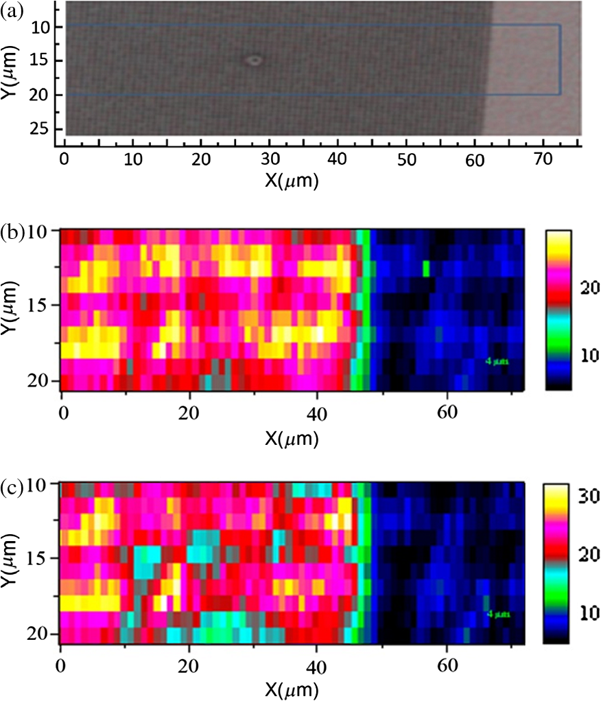 Table 1Average upconversion emission enhancement for samples of Figs. 7 and 8.
Combining the results of Fig. 7 with those of Fig. 8 (see Table 1), the expected emission enhancement due to the gold plasmonic crystal with respect to that of upconversion layer on a glass substrate would be equal to the product of emission enhancement due to the planar gold with respect to glass times that of the plasmonic crystal with respect to planar gold. As a result, the plasmonic crystal enhances the average upconversion emission and at 540 and 665 nm, respectively. The two-photon upconversion emission enhancement is directly proportional to the square of electromagnetic-field intensity. Here we compare the observed upconversion intensity enhancement with that of the electric-field enhancement obtained from FDTD simulations. The maximum simulated electric-field intensity enhancement by gold nanopillar arrays is approximately . However, this enhancement was localized within a small region around the nanopillars (see Fig. 4). The electromagnetic-field intensity, averaged over the thickness of the upconversion layer (105 nm), is enhanced and the average of in the same volume is enhanced by . Nevertheless, experimental measurements show only enhancement (about less than predicted). While the simulation matches the experiment very well in predicting the plasmonic resonance wavelength regime, it falls short in predicting the magnitude of the upconversion enhancement. Part of this discrepancy might be attributed to the following: (1) The nanoparticle film was thinner over gold nanopillars compared to the film planar gold. This would result in overestimation of field enhancement in the simulation. (2) The actual upconverting layer was only 105 nm thick, whereas the simulation model assumed a thick layer (1 μm) of PMMA over the nanopillars. (3) Plane-wave excitation was assumed in the simulation, whereas the excitation in the confocal experiment was a narrow beam focused on a region. 5.Quantitative Analysis of Light-Plasmon-Nanoparticle Interaction: Strategies to Further Enhance Upconversion EnhancementLooking back at Eq. (1), the upconversion emission rate is directly proportional to the excitation rate. The excitation rate (per unit volume per second) in a linear photonic material system at a given point is equal to the product of absorption coefficient (per unit length, normally denoted by ) times photon flux (per unit area per second) at that point. In the case of two-photon upconversion, a second-order nonlinear medium, the absorption coefficient itself, is function of photon flux. In order to decouple the complexity of 3D-FDTD analysis from the complexity of a nonlinear and nonhomogenous medium, we use a narrowband effective medium approximation, using a normalized Lorentz-Lorenz formulation, described in Ref. 38, with an effective real refractive index of and an effective imaginary refractive index of , which relates to the absorption coefficient ( ) by . For the PMMA medium dispersed with -doped nanoparticles, we use an value of 1.6. 39 The value, however, is a function of the intensity of the electromagnetic field. As a result, we adopt a reference imaginary refractive index value of , which is reported for the low-power regime in Ref. 39, for the : 3% Er, 17% Yb material. For a nanoparticle/PMMA composite with a nanoparticle volumetric ratio of 20%, the effective medium approximation leads to effective and values of 1.501 and , respectively. We use as the base imaginary refractive index and use a normalization coefficient of such that . In this study, we sweep the values over a large window to assess the interaction of light–plasmon–nanoparticle as well as the light absorption by nanoparticles and plasmonic resonance. The reference value leads to an absorption coefficient of at 980 nm and penetration depth of 1.67 mm. Such small and values require a very thick (millimeter range) layer of upconversion material. This may not be a cost-efficient method for implementing an upconversion layer, as this layer uses a number of rare-earth elements in high concentration. As demonstrated in Sec. 4, field enhancement by plasmonic resonance can enhance upconversion efficiency; however, plasmonic field enhancement is confined to close proximity to the metal surface. We use a plasmonically enhanced upconversion process through nanostructured metal surfaces to assess whether efficient upconversion can be generated from upconversion layers with a thickness of the order of 1 μm. Figure 9 shows the structure of the volume simulated for absorption and reflection analysis, in which a 1-μm-thick homogenous upconversion layer covers the surface of the gold photonic crystal. Fig. 9Sample volume simulated for absorption and reflection analysis, in which a 1-μm-thick homogenous upconversion layer covers the surface of the gold plasmonic crystal. The plasmonic crystal consists of cylindrical nanopillars in a square lattice with spacing of 620 nm, diameter of 310 nm, and height of 70 nm. 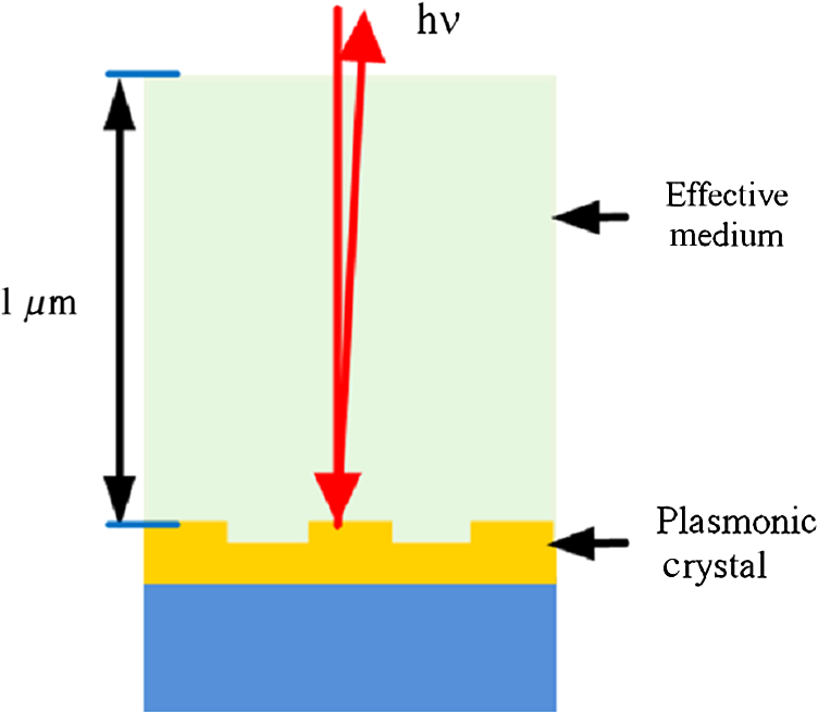 Figure 10 shows the specular reflectance of 980-nm light from the structure in Fig. 9 at normal incident angle as a function of (black squares). Figure 10 also shows the product of and average field intensity (within the upconversion layer) normalized to the incident field intensity (red circles). The simulations show that the excitation rate and, hence, the emission intensity increase linearly with up to the values. In this regime, the upconversion is expected to be limited by excitation rate; i.e., the absorption coefficient in this regime is so low that the upconversion medium can be approximated by a nonabsorbing dielectric layer. For values larger than 1000, however, the excitation and emission rates experience a sublinear growth as a function of . This suggests that absorption by the upconversion layer damps the field intensity. This damping effect can be seen clearly in Fig. 11(a) to 11(c), where the field distributions are plotted for the values of 1, 100, and 10,000, respectively. For values of 1 and 100, the field distribution is very similar to that shown in Fig. 4(a), confirming negligible light absorption by the upconversion layer. For [see Fig. 11(c)], the absorption in the upconversion layer significantly damps the plasmonic field enhancement. This suggests that plasmon-enhanced upconversion is not an efficient approach for a strongly absorbing upconversion medium. Fig. 10Reflectance of 980-nm light from the plasmonic sample of Fig. 9 and product of imaginary refractive index ( ) and average field intensity versus multiples of imaginary refractive index. 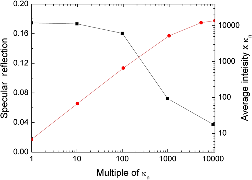 Fig. 11Normalized electric field intensity ( ) around nanopillars when nanoparticles loaded in PMMA had (a) , (b) , and (c) . 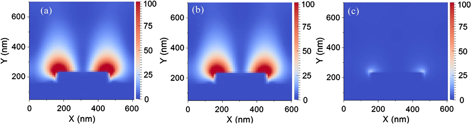 Figure 12 summarizes the result of a comprehensive study on the impact of , which determines the amount of absorption in the upconversion layer, on the normalized magnitude of the average field enhancement for various thicknesses of the upconversion layer. Two key observations can be made. (1) Average field enhancement over the volume of the upconversion layer is higher for thinner films. For a 200-nm-thick effective medium layer, the average field enhancement is at , but decreased to for a 400-nm-thick layer and for a 1-μm-thick layer. (2) There is almost no change in the average electric-field intensity up to for any of the effective medium thicknesses, but a mild attenuation (about 25% decrease) begins between values of 100 and 1000 and strong attenuation is observed for values larger than 1000. Field enhancement even falls below unity for values larger than 10,000. Fig. 12Normalized average electric field intensity ( ) versus multiples of . The average was calculated for different thicknesses of the nanoparticle-PMMA effective medium. 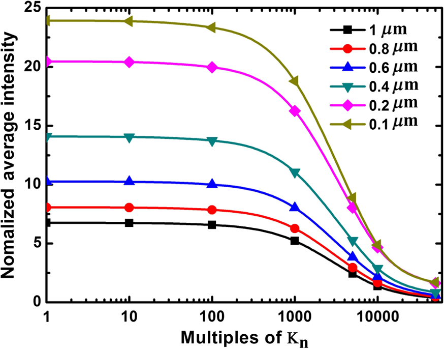 Figure 13 shows the flow of electromagnetic power around a nanopillar in plasmon resonance mode. The energy flow was calculated using Poynting vectors, the real value of , where the direction of arrows shows the direction of the Poynting vectors and the color of the arrows shows the magnitude of the Poynting vectors normalized with respect to the incident power. The arrows show that the energy flows in loops near the nanopillar and back and forth along the metal surface. This indicates that the surface plasmon resonance mode is a standing wave. We use the divergence of the Poynting vector, ), to determine the excitation rate, as well as the spatial distribution of excitations, within the simulated volumes. Figure 14(a) to 14(c) shows the spatial distribution of power absorption around nanopillars, normalized to the thickness of the upconversion layer, for the structure of Fig. 9 with values of 1, 100, and 10,000, respectively. Maximum excitation (white) occurs near the flat surfaces of the nanopillars, indicating that power is flowing toward the nanopillar and is stored in the surface plasmon field. The evanescent plasmon field is associated with the emission of light in the direction of plasmon field decay. 29 In the dark regions, the power absorbed by the nanoparticles is lower than the power emitted by the evanescent field. Therefore, the net divergence of the Poynting vector is negative. Electromagnetic power is also lost due to resistance to plasmonic oscillation in the gold layer. Fig. 13Poynting vector, , plot in -plane normalized with respect to incident power around a single nanopillar. PMMA was a dielectric medium over the gold nanopillars. 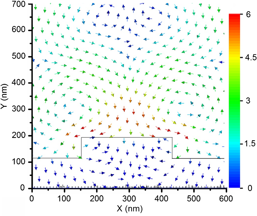 Fig. 14Spatial distribution of energy absorption, , around a nanopillar when the nanopillars were covered with 1-μm-thick nanoparticles-PMMA mix medium for (a) , (b) , and (c) . 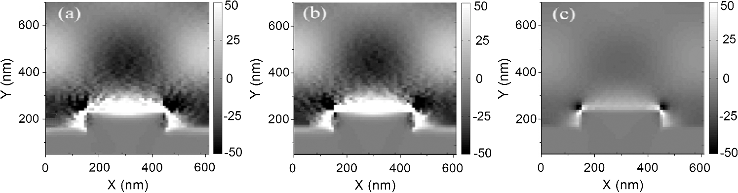 Figure 15 shows the absorption in the upconversion material (proportional to the excitation level) in the plasmonic crystal and the total absorption (sum of absorption in upconversion layer and the plasmonic crystal) over a wide window of values. In these simulations, the thickness of the upconversion layer was kept at 1 μm. The absorption of the upconversion material increases from 6 to 11% when varying from 1 to 100, whereas the absorption of the plasmonic crystal decreases from 58 to 55%. This is the regime in which upconversion efficiency benefits most from plasmonic field enhancement, significantly reducing the required thickness of the upconversion layer. Nevertheless, absorption by the upconversion layer in this regime is much less than that of the plasmonic crystal. A major part of the electromagnetic energy is consumed by resistive losses in this regime. It should be noted that the sum of the absorption components in Fig. 15 and the specular reflection in Fig. 10 for corresponding values is less than unity. The difference originates from the diffraction modes, scattering due to interference of incident light with the plasmonic crystal. When is increased from 100 to 1000, the absorption by the upconversion layer increases but that of the metal layer decreases, intersecting at a value of 43% for an approximate value of 1000. Upon further increase in , the upconversion layer absorbs the majority of the electromagnetic energy and significantly damps the plasmonic activity and, hence, the plasmonic field enhancement. Fig. 15Normalized light absorption in upconverter, gold nanopillars, and gold surface and total absorption versus multiples of . 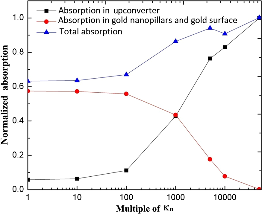 It should be noted that the values can be enhanced in two ways: (1) by increasing the volume fraction of upconversion nanoparticles in PMMA and (2) by increasing the intensity of the incident light, as is directly proportional to the intensity of electromagnetic field. Overall, the simulations outlined here can provide quantitative guidelines for the design and development of efficient upconversion layers. 6.Conclusions2-D periodic arrays of gold nanopillars can enhance the electric-field intensity of incident 980-nm light by in close proximity to the nanopillars and averaged over the volume of a 1-μm-thick dielectric layer due to surface plasmon resonance. These nanopillars showed enhancement of red upconversion emission spectrum in a 105-nm-thick layer of PMMA- : 3% Er, 17% Yb. However, the uniform distribution of nanoparticles in a 1-μm-thick layer of PMMA- : 3% Er, 17% Yb medium could increase this figure several fold. The 3D-FDTD simulations along with the absorption model utilized here showed that over a enhancement in upconversion of 980-nm photons is required for possible consideration of plasmonically enhanced upconversion layer for photovoltaic application, part of which can be achieved by increasing the concentration of nanoparticles in the PMMA matrix. We also showed that the plasmonic upconversion enhancement becomes less efficient due to the loading effect when a highly absorbing upconversion layer is utilized. We conclude that, while plasmon-assisted upconversion enhancement might be used in photodetector applications, new upconversion materials with wideband absorption properties are required for this method to be a promising approach for solar cell applications. AcknowledgmentsThis paper is based upon work supported by the National Science Foundation/EPSCoR Grant No. 0903804 and by the state of South Dakota. The authors would like to acknowledge the Nanofabrication Center, a node of National Nanotechnology Infrastructure Network at the University of Minnesota, for access to the electron-beam lithography and electron-beam evaporation systems. The authors acknowledge Lynn Gedvilas of the Electro-optics Characterization group at National Renewable Energy Laboratory for making the reflectivity measurements. References
M. A. Green
,
“Thin-film solar cells: review of materials, technologies and commercial status,”
J. Mater. Sci: Mater. Electron., 18 S15
–S19
(2007). http://dx.doi.org/10.1007/s10854-007-9177-9 0957-4522 Google Scholar
M. F. Baroughi
S. Sivoththaman
,
“A novel silicon solar cell using a low temperature quasi-epitaxial silicon emitter,”
IEEE Electron Device Lett., 28
(7), 575
–577
(2007). http://dx.doi.org/10.1109/LED.2007.897873 0741-3106 Google Scholar
T. Searle
, Properties of Amorphous Silicon, and Its Alloys, INSPEC/Institution of Electrical Engineering(1998). Google Scholar
A. Fahrenbruch
,
“Modeling results for CdS/CdTe solar cells,”
(2000). Google Scholar
B. E. McCandless
J. R. Sites
,
“Cadmium telluride solar cells,”
Handbook of Photovoltaic Science and Engineering, John Wiley & Sons, England
(2003). Google Scholar
M. Gloeckler
A. L. Fahrenbruch
J. R. Sites
,
“Numerical modeling of CIGS and CdTe solar cells: setting the baseline,”
in Proc. of 3rd World Conf. on Photovoltaic Energy Conversion,
491
–494
(2003). Google Scholar
M. Gratzel
,
“Nanaocrystalline injection solar cells,”
Thin Film Solar Cells, John Wiley & Sons Ltd., England
(2006). Google Scholar
B. Bills
S. Mariyappan
M. F. Baroughi
,
“Effects of atomic layer deposited
compact layer on the performance of dye-sensitized solar cells,”
Thin Solid Films, 519
(22), 7803
–7808
(2011). http://dx.doi.org/10.1016/j.tsf.2011.05.007 0040-6090 Google Scholar
V. D. Mihailetchi
et al.
,
“Charge transport and photocurrent generation in poly(3-hexylthiophene): methanofullerene bulk heterojunction solar cells,”
Adv. Funct. Mater., 16
(5), 699
–708
(2006). http://dx.doi.org/10.1002/(ISSN)1616-3028 1616-3028 Google Scholar
T. Trupke
M. A. Green
P. Würfel
,
“Improving solar cell efficiencies by up-conversion of sub-band-gap light,”
J. Appl. Phys., 92
(7), 4117
–4122
(2002). http://dx.doi.org/10.1063/1.1505677 0021-8979 Google Scholar
C. Lin
et al.
,
“Highly luminescent NIR-to-visible upconversion thin films and monoliths requiring no high-temperature treatment,”
Chem. Mater., 21
(14), 3406
–3413
(2009). http://dx.doi.org/10.1021/cm901094m 0897-4756 Google Scholar
H. P. Paudel
et al.
,
“Geometric dependence of field enhancement in 2D metallic photonic crystals,”
Opt. Express, 17
(24), 22179
–22189
(2009). http://dx.doi.org/10.1364/OE.17.022179 1094-4087 Google Scholar
H. P. Paudel
et al.
,
“Enhancement of electromagnetic field intensity by metallic photonic crystal for efficient upconversion,”
in 35th IEEE Photovoltaic Specialists Conf.,
002938
–002942
(2010). Google Scholar
H. P. Paudel
K. Bayat
M. F. Baroughi
,
“Plasmon resonance modes in two dimensional arrays of metallic nanopillars,”
JOSA B, 27
(9), 1693
–1697
(2010). http://dx.doi.org/10.1364/JOSAB.27.001693 0740-3224 Google Scholar
E. Rephaeli
S. Fan
,
“Absorber and emitter for solar thermo-photovoltaic systems to achieve efficiency exceeding the Shockley-Queisser limit,”
Opt. Express, 17
(17), 15145
(2009). http://dx.doi.org/10.1364/OE.17.015145 1094-4087 Google Scholar
Z. Yu
A. Raman
S. Fan
,
“Fundamental limit of nanophotonic light trapping in solar cells,”
PNAS, 107 17491
–17496
(2010). http://dx.doi.org/10.1073/pnas.1008296107 0027-8424 Google Scholar
X. H. Li
et al.
,
“Light extraction efficiency and radiation patterns of III-nitride light-emitting diodes with colloidal microlens arrays with various aspect ratios,”
IEEE Photon. J., 3
(3), 489
–499
(2011). http://dx.doi.org/10.1109/JPHOT.2011.2150745 1943-0655 Google Scholar
M. A. Tsai
et al.
,
“Enhanced conversion efficiency of a crystalline silicon solar cell with frustum nanorod arrays,”
Opt. Express, 19
(Suppl 1), A28
–A34
(2011). http://dx.doi.org/10.1364/OE.19.000A28 1094-4087 Google Scholar
A. Polman
H. A. Atwater
,
“Photonic design principles for ultrahigh-efficiency photovoltaics,”
Nat. Mater., 11 174
–177
(2012). http://dx.doi.org/10.1038/nmat3263 1476-1122 Google Scholar
Q. Gan
F. J. Bartoli
Z. H. Kafafi
,
“Plasmonic-enhanced organic photovoltaics: breaking the 10% efficiency barrier,”
Adv. Mater., 25
(17), 2385
–2396
(2013). http://dx.doi.org/10.1002/adma.v25.17 0935-9648 Google Scholar
N. C. Das
,
“Tunable infrared plasmonic absorption by metallic nanoparticles,”
J. Appl. Phys., 110
(4), 046101
(2011). http://dx.doi.org/10.1063/1.3624596 0021-8979 Google Scholar
H. Zhao
et al.
,
“Surface plasmon dispersion engineering via double-metallic Au/Ag layers for III-nitride based light-emitting diodes,”
Appl. Phys. Lett., 98
(15), 151115
(2011). http://dx.doi.org/10.1063/1.3580628 0003-6951 Google Scholar
J. Henson
et al.
,
“Plasmon-enhanced light emission based on lattice resonances of silver nanocylinder arrays,”
Opt. Lett., 37
(1), 79
–81
(2012). http://dx.doi.org/10.1364/OL.37.000079 0146-9592 Google Scholar
M. Moskovits
,
“Surface-enhanced spectroscopy,”
Rev. Mod. Phys., 57
(3), 783
–826
(1985). http://dx.doi.org/10.1103/RevModPhys.57.783 0034-6861 Google Scholar
J. R. Lakowicz
,
“Radiative decay engineering: biophysical and biomedical applications,”
Anal. Biochem., 298
(1), 1
–24
(2001). http://dx.doi.org/10.1006/abio.2001.5377 0003-2697 Google Scholar
G. Bauer
et al.
,
“Resonant nanocluster technology—from optical coding and high quality security features to biochips,”
Nanotechnology, 14 1289
–1311
(2003). http://dx.doi.org/10.1088/0957-4484/14/12/010 0957-4484 Google Scholar
J. R. Lakowicz
,
“Radiative decay engineering 5: metal-enhanced fluorescence and plasmon emission,”
Anal. Biochem., 337
(2), 171
–194
(2005). http://dx.doi.org/10.1016/j.ab.2004.11.026 0003-2697 Google Scholar
S. A. Maier
, Plasmonics: Fundamentals and Applications, Springer, New York
(2007). Google Scholar
E. Fort
S. Gresillon
,
“Surface enhanced fluorescence,”
Appl. Phys., 41
(1), 013001
(2008). http://dx.doi.org/10.1088/0022-3727/41/1/013001 1080-9198 Google Scholar
J. A. Schuller
et al.
,
“Plasmonics for extreme light concentration and manipulation,”
Nat. Mater., 9 193
–204
(2010). http://dx.doi.org/10.1038/nmat2630 1476-1122 Google Scholar
J. Song
et al.
,
“Large enhancement of fluorescence efficiency from CdSe/ZnS quantum dots induced by resonant coupling to spatially controlled surface plasmons,”
Nano Lett., 5
(8), 1557
–1561
(2005). http://dx.doi.org/10.1021/nl050813r 1530-6984 Google Scholar
D. M. da Silva
et al.
,
“Frequency upconversion in
doped
glasses containing metallic nanoparticles,”
App. Phys. Lett., 90
(8), 081913
(2007). http://dx.doi.org/10.1063/1.2679798 0003-6951 Google Scholar
T. Aisaka
M. Fujii
S. Hayashi
,
“Enhancement of upconversion luminescence of Er doped
films by Ag island films,”
App. Phys. Lett., 92
(13), 132105
(2008). http://dx.doi.org/10.1063/1.2896303 0003-6951 Google Scholar
S. Schietinger
et al.
,
“Plasmon-enhanced upconversion in single
codoped nanocrystals,”
Nano Lett., 10
(1), 134
–138
(2010). http://dx.doi.org/10.1021/nl903046r 1530-6984 Google Scholar
H. P. Paudel
et al.
,
“Enhancement of near-infrared-to-visible upconversion luminescence using engineered plasmonic gold surfaces,”
J. Phys. Chem. C, 115
(39), 19028
–19036
(2011). http://dx.doi.org/10.1021/jp206053f 1932-7447 Google Scholar
A. Taflove
, Computational Electrodynamics: Finite-Difference Time-Domain Method, Artech House Inc., Norwood, Massachusetts
(1995). Google Scholar
H. P. Paudel
,
“Enhancement of light-plasmons-nanoparticle interaction for upconversion applications in solar cells,”
South Dakota State University, Brookings,
(2011). Google Scholar
U. Kreibig
M. Vollmer
, Optical Properties of Metal Clusters, Springer-Verlag, New York
(1995). Google Scholar
R. H. Page
et al.
,
“Upconversion-pumped luminescence efficiency of rare-earth-doped hosts sensitized with trivalent ytterbium,”
J. Opt. Am. B, 15
(3), 996
–1008
(1998). http://dx.doi.org/10.1364/JOSAB.15.000996 0740-3224 Google Scholar
|