|
|
1.IntroductionThe efficiency enhancement of silicon solar cells by increasing the interaction length of light at weakly absorbed wavelengths using backside diffraction gratings has been widely studied. 1 – 10 However, several aspects that require systematic in-depth analysis have not been sufficiently addressed so far. We have recently introduced a simulation procedure 11 – 13 combining a two-dimensional ray tracing algorithm with rigorous coupled wave analysis (RCWA) that facilitates comprehensive studies on the efficiency enhancement in silicon solar cells by means of backside diffraction gratings. Compared to the fully electromagnetic simulation methods, RCWA and finite difference time domain (FDTD), the major benefit of this combined approach is the strongly reduced computation time and the gain in simulation precision, in particular for cells with an absorber thicker than 10 μm. Previously, we have already applied this combined RCWA/ray tracing approach to study the influence of the absorber thickness on the optimum grating parameters providing maximum photocurrent densities. 11 In this article, we present an in-depth analysis of the influence of simulation parameters, such as the recursion depth or the diffraction order and the number of diffraction orders on the simulation outcomes. This analysis not only reveals the requirements for achieving a correct optimization of the grating parameters but also provides unprecedentedly a clear picture of the light trapping mechanism. Furthermore, for the first time to the best of our knowledge, we investigate the influence of the angle of incidence of sunlight on the optimum parameters of backside gratings. 2.Simulation Method and Coherence of SunlightFigure 1 shows the silicon solar cell model with a backside diffraction grating investigated in this article and a reference structure without grating. In this article, we exclusively use a duty cycle of the diffraction gratings which is 1:1. The flat front surface is covered with a single layer antireflection (AR) coating made of 80-nm silicon nitride (SiNx). The backside is covered with a 100-nm-thin layer and an aluminum electrode. The layer improves the reflectance of the backside aluminum electrode. Fig. 1Investigated silicon solar cell models (a) with and (b) without backside diffraction grating (reference cell).  In our approach, the front side thin film AR coating and the backside diffraction grating including a thin film coating are treated in a fully coherent way, whereas the silicon layer is treated incoherently. In a first step, the reflectivity and transmissivity of the front side AR coating were calculated as polarization dependent functions of the angle of incidence and employing the standard equations for a homogeneous dielectric film. 14 Furthermore, the diffraction efficiencies of the backside gratings were also determined for different period lengths and modulation depths depending on the angle of incidence, wavelength, polarization, and diffraction order by means of RCWA. All these resulting data were interpolated to accelerate the computation in the subsequent ray tracing, in which the overall light absorption inside the silicon was calculated. In this ray tracing algorithm, light rays with different wavelengths entering the silicon layer are traced for a certain number of zig-zag reflections inside the silicon layer. The recursion depth counts the number of reflections at the backside grating of each light ray, taken into account for calculating the absorption. In our simulations, each ray is traced inside the silicon layer until either its fractional intensity is smaller than a minimum limit ( ) or the number of reflections/diffractions at the backside grating exceeded the recursion depth . The ray tracing is performed for different wavelengths and for both polarizations. As the light rays propagate inside the silicon layer the wavelength dependent absorption is summed up according to Beer–Lambert’s law. 11 Finally, the absorption was integrated over the wavelength range 300 to 1140 nm, and averaged over both polarizations. The photocurrent density is defined by where is the photon absorption inside the silicon, is the incident photon flux, and e is the elementary charge. 11 In this article, the photocurrent density was calculated by summing up the number of absorbed photons over the solar spectrum air mass coefficent (AM 1.5). over both polarizations. It was assumed that each absorbed photon generates an electron hole pair without considering electrical losses.Green’s complex refractive index data for silicon are used, 15 and for the complex refractive index data of Al and were used. 16 – 18 Further details on this combined RCWA/ray tracing approach can be found in Refs. 11 12.–13 and 19. This combined coherent/incoherent approach can be justified in the following way. The coherence length of sunlight measured by means of a Michelson interferometer has been estimated to be about 600 nm, under the assumption that the sun is a black body radiator emitting photons at temperature of . 20 It is often argued that for optical path lengths longer than this coherence length no interference occurs and, therefore, an incoherent treatment is appropriate. From this point of view the incoherent treatment of silicon layers with a thickness of would be well justified. However, in fact etalons of several microns thickness still act as thin film filters which are well known to increase the coherence length. 21 Therefore, it can be expected that Fabry–Perot resonances also occur for silicon layers of several microns thickness. In this partially coherent regime, the fringe visibility of the Fabry–Perot resonances will decrease with increasing layer thickness. Moreover, the spectral distance between two resonances decreases with increasing silicon layer thickness. In terms of absorption and, thus, photocurrent, the effect of these Fabry–Perot resonances is negligible, and an incoherent treatment of the silicon layer is acceptable. In order to validate the combined RCWA/ray tracing approach, we compared the simulation outcomes of the photocurrent densities with the results obtained by a full RCWA simulation for thin cells. Figure 2 plots the absorption spectra calculated by the combined RCWA/ray tracing approach and the absorption spectra obtained from fully coherent RCWA simulations for thin cells with thicknesses of 1, 3, and 10 μm as well as the spectra for the corresponding reference cells without grating (dashed curves). For both methods, the results of the two polarizations [transverse electric (TE) and transverse magnetic (TM)] were averaged. In the combined RCWA/ray tracing approach, a recursion depth of was chosen and the highest order of diffraction taken into account was set to . Fig. 2Absorption spectra calculated by the combined rigorous coupled wave analysis (RCWA)/ray tracing approach and by full RCWA simulations averaged for TE and TM polarization for thin silicon solar cells with a thickness of 1, 3, and 10 μm. The dashed red lines indicate the results of the combined RCWA/ray tracing approach for cells without backside grating (w.g.). The symbol # indicates the number of harmonics used for the RCWA simulations.  The absorption spectra calculated with full RCWA (blue curves in Fig. 2) show oscillations caused by interference effects inside the silicon while for the spectra calculated with the combined RCWA/ray tracing approach these interference effects are taken into account. In particular for thin cells, strong oscillations due to interference effects occur under the assumption of a coherent light. These oscillations are largely averaged out in the calculation of the photocurrent densities. The deviations of the photocurrent densities between the two methods amount to about 4% for , 1.7% for , and 0.9% for . Thus, with increasing silicon thickness the differences get smaller because interference effects play a less important role. A significant advantage of the combined simulation method is that the RCWA-based calculation of the backside grating diffraction efficiency can be performed for a thin simulation domain without including the absorber layer. This allows the use of a sufficiently large number of harmonics, in this article 35, guaranteeing a high precision of the simulation outcomes independent of the silicon absorber thickness. By contrast, the precision of full RCWA simulations of the whole solar cell structure including the absorber layer will drop rapidly for thicknesses exceeding a few microns, because the number of harmonics has to be reduced due to limitations in computer memory and computation time. Therefore, especially for cells with a thickness the combined RCWA/ray tracing simulation approach is highly favourable compared to full electromagnetic simulation methods, such as RCWA and FDTD because, the simulations can be performed with a sufficiently large number of harmonics. As an additional benefit, the incoherent treatment of the silicon absorption layer provides a much better physical insight into the light trapping mechanism, which cannot be gained when using fully coherent simulation methods, where Fabry–Perot resonances obscure the characteristic humps in the absorption spectra (see Fig. 2) which will be described in detail in Sec. 3. 3.Light Trapping Mechanism in Silicon Solar Cells with Backside Diffraction GratingsLight trapping by means of backside diffraction gratings relies on the deflection of incident light to propagation angles above the critical angle of total internal reflection ( ). This can considerably enhance the interaction length and, thus, the absorption of light within the silicon layer. The diffraction angles inside the silicon layer of the solar cell can be calculated by where is the wavelength, is the angle of incidence on the solar cell front side in air, is the diffraction order, is the grating period, and is the refractive index of silicon. 22 In addition, the following inequality has to be fulfilled which means that for a given grating period and diffraction order there is an upper wavelength limit above which no diffraction can occur. 22Figure 3(a) plots the wavelength dependent angles of first-order diffraction ( ) for different grating periods (400 to 1000 nm) in the case of normal incident light calculated by Eq. (1). From this equation, it follows that for normal incident light ( ) the diffraction angle equals the angle of TIR, , if . Two regions can be distinguished: in region I ( ), the diffraction angles are smaller than the and, thus, lie within the escape cone [see Fig. 1(a)], where no significant light trapping can occur; in region II ( ), the diffraction angles are larger than and, therefore, all rays are totally reflected at the front surface back into the silicon for further absorption. According to Eq. (2) for higher diffraction orders the angle of diffraction exceeds at much shorter wavelengths. For example, in Fig. 3(a) the line representing the diffraction angles for the case and corresponds to the case and . Fig. 3(a) First-order diffraction angles and angle of TIR at the Si/SiNx/air interface (red curve); (b) calculated absorption spectra averaged over TE and TM polarization in silicon solar cells with planar backside electrode (dashed lines) and with optimized backside gratings for silicon thicknesses ranging from 1 to 200 μm. For 1 μm thickness the absorption spectra of TE and TM polarization are also plotted separately.  Figure 3(b) shows the calculated absorption spectra of silicon solar cells with backside gratings optimized for different thicknesses ranging from 1 to 200 μm in the case of normal incident light. 11 The results were obtained for a recursion depth of , which provided the best compromise between accuracy and computation time. The highest order of diffraction taken into account was set to 5. Further details on the influence of these parameters will be given in Secs. 4 and 5. The absorption spectra in Fig. 3(b) provide additional insight into the light trapping effect. Significant absorption humps occur in distinctive wavelength regions which are related to the optimized grating periods. At wavelengths similar to the respective optimized grating period, the absorption significantly rises. At higher wavelengths, the humps have a falling slope where the enhancement drops abruptly but the absorption still remains at values higher than that of solar cells without grating indicated by dashed lines. In the following, the light trapping mechanism and the origin of the humps will be analyzed in more detail for solar cells with thicknesses of 1 μm. As can be seen from Fig. 3(b), the shapes of the absorption spectra for TE and TM polarization show very similar behavior because the underlying diffraction mechanism is the same. We therefore restrict this analysis to TE polarization without loss of generality. Figure 4(d) plots the spectral diffraction efficiencies of normal incident TE polarized light for the optimized grating structure ( , ) and . For reasons of symmetry, the diffraction efficiencies of the negative orders ( ) are the same for . In the spectral region with wavelengths slightly larger than the optimized grating periods, the zero-order diffraction efficiencies strongly decrease, while the first-order diffraction efficiencies rise sharply. The rising slope of the hump is caused by the increasing first-order diffraction angle [see Fig. 3(a)], which translates into a higher reflectivity at the upper interface with increasing wavelength peaking at , where TIR occurs. Light with is totally internally reflected back into the silicon resulting in a longer interaction length and, therefore, larger absorption. Fig. 4(a), (b), and (c) Calculated absorption spectra of TE polarized light in a 1-μm-thin silicon solar cell with optimized diffraction grating ( , ) for recursion depth , 2, and 3 taking into account different numbers of diffraction orders ; (d), (e), and (f) spectral diffraction efficiencies of different diffraction orders for angles of incidence , , and . 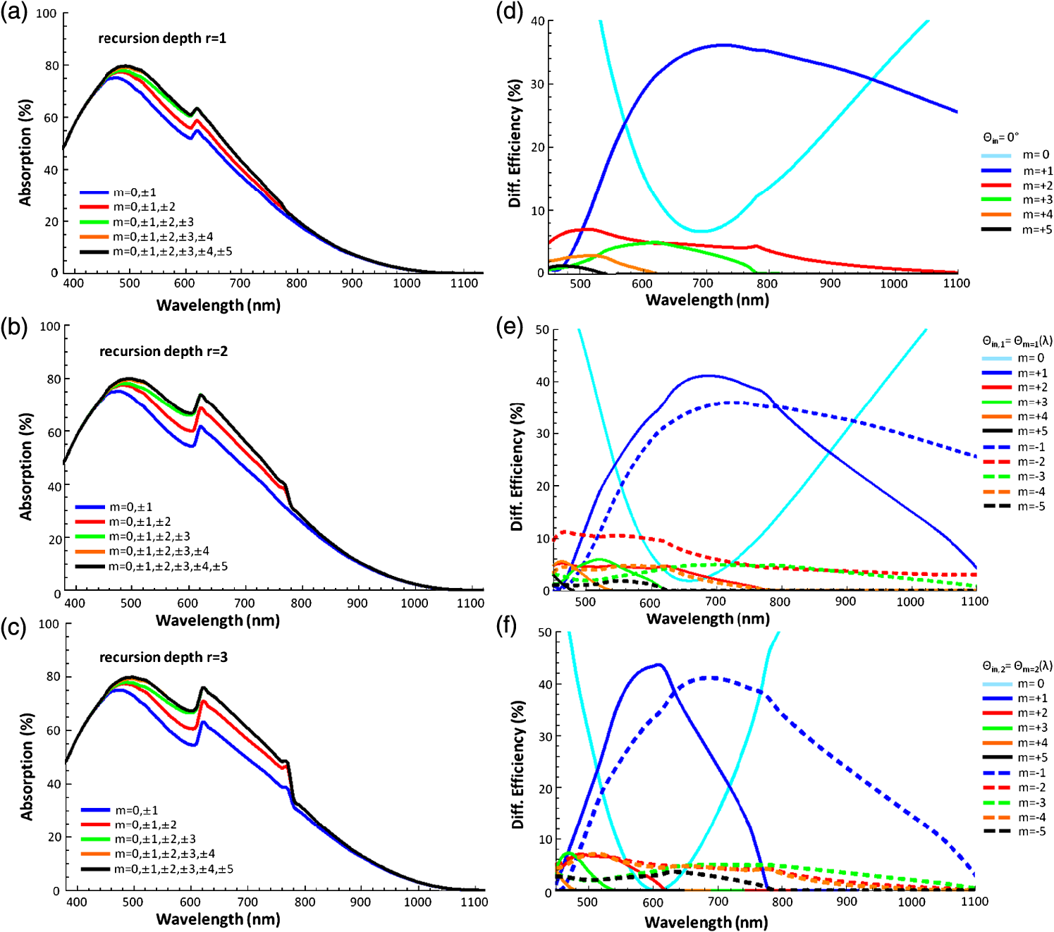 The abruptly falling slopes of the humps in the absorption spectra of Fig. 3(b) can be explained by the limit of diffraction given by Eq. (2), where the diffraction angle for a certain diffraction order approaches 90 deg. Above this cut-off wavelength no diffraction can occur. The interaction length of rays diffracted to large angles increases dramatically, thus resulting in a strong contribution even though the diffraction efficiency might be comparatively low. This fact is illustrated by Fig. 5(a), which plots the diffraction angles on a grating with as a function of wavelength for the discrete angle of incidences. Figure 5(a) clearly shows that for higher diffraction orders, which are indicated by the subscript index, the corresponding diffraction angles given by Eq. (2) reach the limit of diffraction at much smaller wavelengths compared to lower diffraction orders. For comparison the angle of TIR is also inserted in Fig. 5(a) (red colored line). Figure 5(b) shows the enhancement of the single round trip (SRT) interaction length for photons with diffraction angles ( ) larger than the . The enhancement of the SRT interaction length is given by the ratio between the optical path length from the point of diffraction at the grating to the next incidence on the grating and , which represents the SRT interaction length for normal incidence in a solar cell with a planar backside. This enhancement amounts to . Fig. 5(a) Diffraction angle spectrum in a silicon solar cell with a backside grating of period . (b) Optical path length enhancement of normally incident light for SRT from the first to the second diffraction at the backside grating in multiples of the path length ( ). 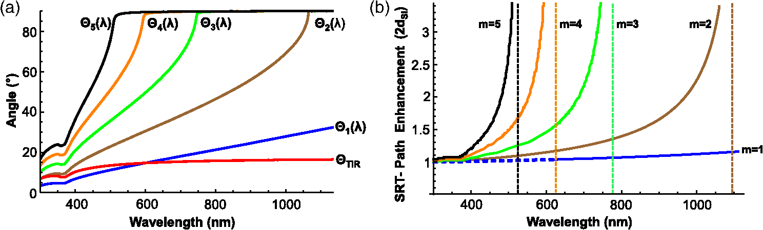 In the following, we discuss the origin of the falling slope of the hump in the absorption spectrum in more detail for the diffraction grating with a period of and a modulation depth of . For this grating the abruptly falling slope occurs near the wavelength of 780 nm. In Figs. 4(a)–4(c) the associated absorption spectra are plotted for different recursion depths and maximum diffraction orders taken into account. Figures 4(d)–4(f) plot the efficiencies of different diffraction orders for three distinctive angles of incidences on the grating , , and , respectively. The angles of incidences and occur if normal incident photons are diffracted into the first ( ) or second diffraction order ( ), respectively, get reflected at the front side, and again hit the grating. One finds that for the recursion depth the falling slope appears if diffraction up to the third-order is taken into account ( ). For the recursion depth , the falling slope becomes observable if diffraction up to the second-order is considered ( ). Accordingly, for recursion depth the falling slope can be found already if only first-order diffraction ( ) is taken into account. This behavior can be explained by the fact that in all three cases the diffraction efficiencies of the corresponding highest considered diffraction orders become zero for wavelengths , i.e., where becomes 90 deg. The diffraction angle can be reached for normal incident light ( ) by third-order diffraction ( ), or for light incident with by second-order diffraction ( ), or for light incident with by first-order diffraction ( ). The first case can occur already for a recursion depth with , whereas the second case requires a diffraction into , which only can occur for recursion depth . If the order of diffractions taken into account is limited to , the third case can only occur for at least three interactions of the ray with the grating, i.e., . As can be seen in Fig. 3(b), the humps in the absorption spectra of thin solar cells with optimized backside gratings occur at much shorter wavelengths than that of thicker cells. The reason for this behavior is given by the fact that in thin cells even short wavelength photons, which have a stronger contribution to the solar spectrum, can reach the backside diffraction grating before getting absorbed inside the silicon layer. The comparison of the absorption spectra in Fig. 3(b) clearly shows that the light trapping effect is most pronounced for thin solar cells. With increasing silicon thickness, the wavelengths of the photons relevant for light trapping become longer. Since the solar light is much less intensive in this long wavelength region, the absorption enhancement is significantly smaller. Nevertheless, diffraction gratings can be used for increasing the photocurrent densities of cells with thicknesses of 200 μm or thicker. For a thickness of 1 μm the photocurrent of a solar cell with an optimized backside grating is increased by about 35% with respect to that of a solar cell without backside grating. For a thickness of 200 μm the photocurrent enhancement still amounts to about 3.9%. 11 4.Investigation of the Recursion DepthIn this section, the influence of the recursion depth on the photocurrent density as well as on the optimized diffraction grating parameters is investigated for silicon solar cells with thicknesses of 1, 10, 100, and 200 μm. Figure 6 plots the photocurrent densities for these cells dependent on the grating period and modulation depth for different recursion depths ( , 2, 3, 8). Bright areas indicate geometries with relatively high photocurrent densities while dark areas correspond to geometries with relatively low photocurrent densities. The optimized diffraction grating parameters and photocurrent densities dependent on the recursion depth ranging from 1 up to 8 are summarized in the tables of Fig. 6. The simulation results show that the optimum grating period for the 1- and 10-μm-thick cells undergo a significant shift to smaller values for recursion depths of , , and compared with recursion depth . Simulations performed for the 1-μm-thick cell with a recursion depth result in the same optimized grating period , while the optimum period is 275 nm for , 575 nm for , and 600 nm for . Simulations performed for the 10-μm-thick cell with a recursion depth result in the same optimized grating period , while the optimum period is 375 nm for , 775 nm for , and 800 nm for . For the thicker cells with and 200 μm, a recursion depth of is sufficient for identifying the optimum grating parameters. The difference in the optimized grating parameters for compared with can be as large as 500 nm for the period and 175 nm for the modulation depth. Fig. 6Photocurrent densities of silicon solar cells with thicknesses of 1, 10, 100, and 200 μm as a function of grating period and modulation depth for four different recursion depths , 2, 3, 8. The grating period was varied from 250 nm up to 1.25 μm and the modulation depth from 25 nm up to 400 nm in steps of 12.5 nm. The tables give the optimized grating parameters obtained for a certain recursion depth and the corresponding photocurrent densities. 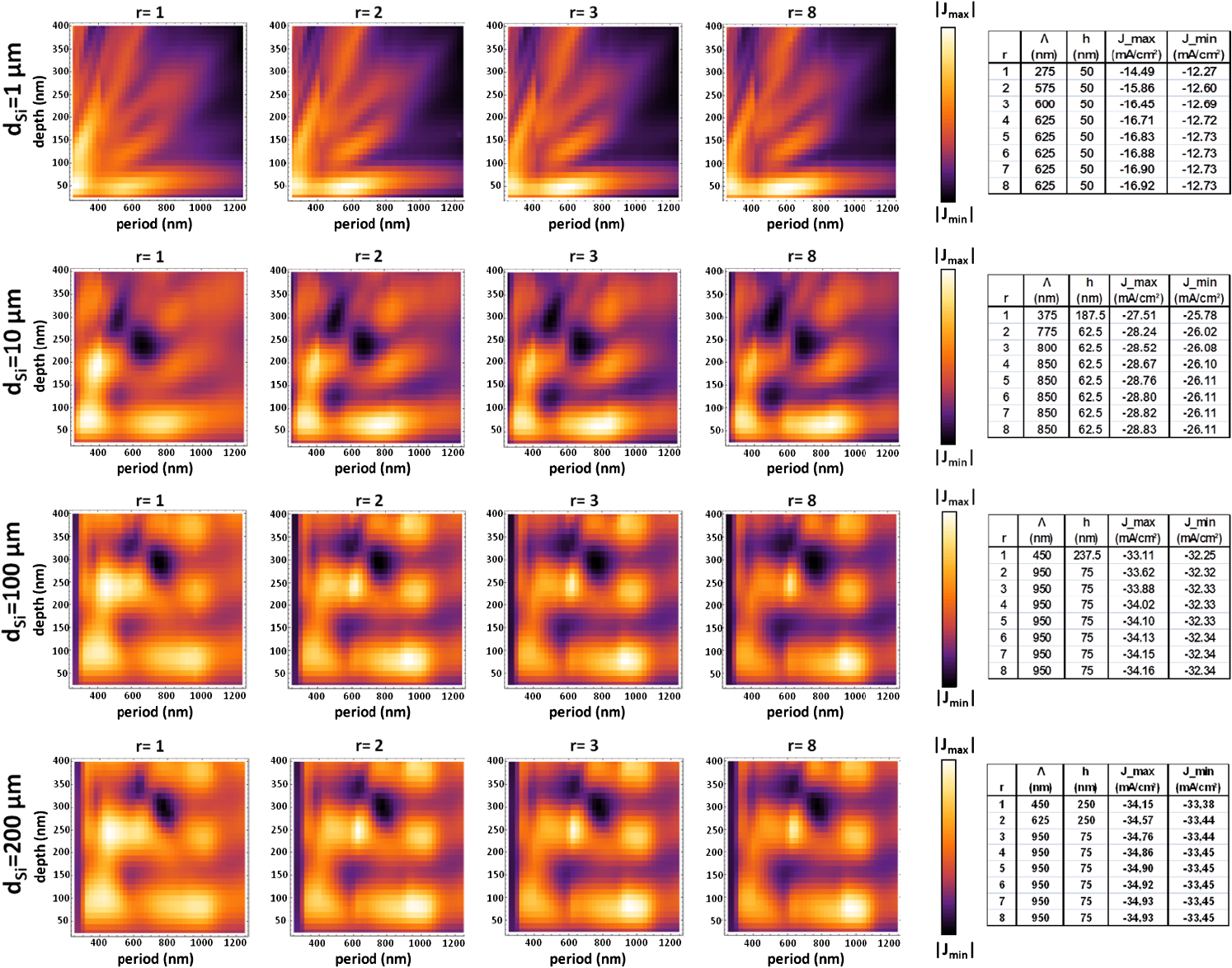 The reason for the shift of the optimized grating period with increasing recursion depth is that a low recursion depth underestimates the contribution of longer wavelengths to absorption and, therefore, the potential of light trapping will not be fully exploited. A low recursion depth in the combined RCWA/ray tracing simulation favors shorter wavelengths and consequently shorter grating periods. By including higher orders of recursion, the absorption of long wavelength photons increasingly contribute to the overall absorption. This relationship becomes apparent from Figs. 7(a)–7(c), which plot the absorption spectra of 1-, 10-, and 200-μm-thick silicon solar cells with optimized gratings for recursion depths ranging from up to . For the 1-μm-thick cell, differences in the simulated absorption curves occur already at wavelengths of about 550 nm, where the solar spectrum has its maximum. For the 200-μm-thick cell deviations of the absorption, curves start to appear at much higher wavelengths near 1000 nm, where intensity of the solar spectrum is much lower. For a recursion depth of the absorption spectra and, thus, the photocurrent densities nearly converge. The absorption spectra for plotted in Figs. 7(a)–7(c) are almost indistinguishable, which suggests that a recursion depth of is sufficient for in-depth analyses of the photocurrent densities. Simulations performed with require a significantly larger calculation capacity and therefore result in extremely long computation times. In our study, a recursion depth of turned out to provide the best compromise between accuracy in terms of grating optimization and computation time. The differences between the photocurrent densities for the optimized grating geometry calculated with and amount to for thin cells ( ), for , and for the thicker cells ( ). Fig. 7(a), (b), and (c) Absorption spectra of optimized diffraction gratings for 1, 10, and 200-μm-thick silicon solar cells with different recursion depths ( ); (d), (e), and (f) photocurrent densities of optimized gratings calculated by simulations with (black curves) as well as for gratings optimized with (red curves) and (blue curve) as a function of the recursion depth. 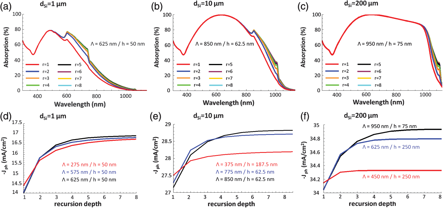 Figures 7(d)–7(f) plot the photocurrent densities of solar cells with optimized grating geometries, which were obtained for a recursion depth of (black curves), as function of the recursion depth for the corresponding cell thicknesses 1, 10, and 200 μm. In order to emphasize the importance of choosing a sufficiently high recursion depth the figures also include the photocurrent densities and of solar cells with wrongly optimized grating parameters obtained for (red curve) and (blue curve), respectively. With increasing recursion depth the photocurrent densities rise relatively more strongly and overtake the initially higher values of and . The differences of the calculated photocurrent densities and amount to for the 1-μm-thick cell, to for -thick cell, and to for the 200-μm-thick cell. Optimizing the grating geometry with an insufficient recursion depth not only results in a lower theoretical photocurrent enhancement but also falsely predicts gratings with shorter periods and higher modulation depths (see tables in Fig. 6). From a practical point of view this puts higher technical demands on the fabrication process. These results suggest that for the determination of the optimum diffraction grating design the proper choice of the recursion depth is highly important and that, in particular, simulations performed with a recursion depth of can lead to wrong optimized grating parameters not fully exploiting the potential of the light trapping effect. This conclusion is of high relevance because other research groups limit their studies to a recursion depth of , i.e., taking into account only the first backside diffraction at the gratings (e.g., Refs. 4, 10). 5.Investigation of the Diffraction OrderIn this section, the influence of the number of diffraction orders on the optimized diffraction grating parameters is investigated for silicon solar cells with 1, 10, and 200 μm thickness for a recursion depth of . The simulation results shown in Figs. 4(a)–4(c) indicate that convergence is ensured if diffraction orders up to are taken into account. Moreover, from Eq. (2) it follows that the cut-off wavelength above which no diffraction can occur for becomes extremely short [compare also the cut-off wavelength of the fifth diffraction order in Fig. 4(d)]. Therefore, contributions of these higher diffraction orders can be neglected for silicon solar cells. Figure 8 plots the photocurrent densities as functions of the grating period Λ and the modulation depth in dependence of the number of diffraction orders taken (up to ) for different silicon thickness. The corresponding optimized grating parameters are given below each plot in Fig. 8. The results indicate that at least three diffraction orders for the 10- and 200-μm-thick cells and four diffraction orders for the 1-μm-thick silicon solar cell have to be included for the evaluation of the optimized diffraction gratings. Simulations performed with a lower number result in wrong optimized grating parameters with strongly reduced period lengths. 6.Simulation Results for Oblique Light IncidenceSo far, the optimization of silicon solar cells with backside diffraction gratings has only been investigated for normally incident light. In the following, the influence of the angle of incidence on the optimized grating parameters will be studied. For this purpose, a systematic optimization of the grating geometry for angles of incidence on the solar cell of 0 deg to 70 deg was performed in 10 deg steps. For each angle of incidence, the period was varied from 0.25 to 1.25 μm and the modulation depth from 25 to 400 nm, both in steps of 12.5 nm. This optimization was carried out for 1-, 10-, and 200-μm-thick silicon solar cells. The results showed that the optimized grating geometries do not depend on the angle of incidence. Figure 9 plots the photocurrent densities for 1-, 10-, and 200-μm-thick silicon solar cells dependent on the period length and the modulation depth for normally incident light as well as for . These figures clearly indicate that the optimized grating geometry does not depend on the angle of incidence on the solar cell. This can be explained by the law of refraction and the high refractive index of silicon, which concentrates all possible angles of incidence to the narrow escape cone inside silicon. Even sunlight shining on the solar cell under a glancing angle will hit the backside grating with a steep angle of incidence below the , which is for silicon [see red curve of Fig. 3(a)]. Since the diffraction efficiencies of backside gratings for normally incident photons, and photons hitting the grating under small angles of a few degrees are very similar, they do not influence the optimized grating parameters. Fig. 9(a)–(f) Photocurrent densities for 1, 10, and 200-μm-thick silicon solar cells as a function of the period and modulation depth for angles of incidence deg and ; (g) and (h) absorption spectra of 1, 10, and 200-μm-thick silicon solar cells with optimized gratings for angles of incidence on the solar cell ranging from 0 deg to 70 deg in steps of 10 deg. 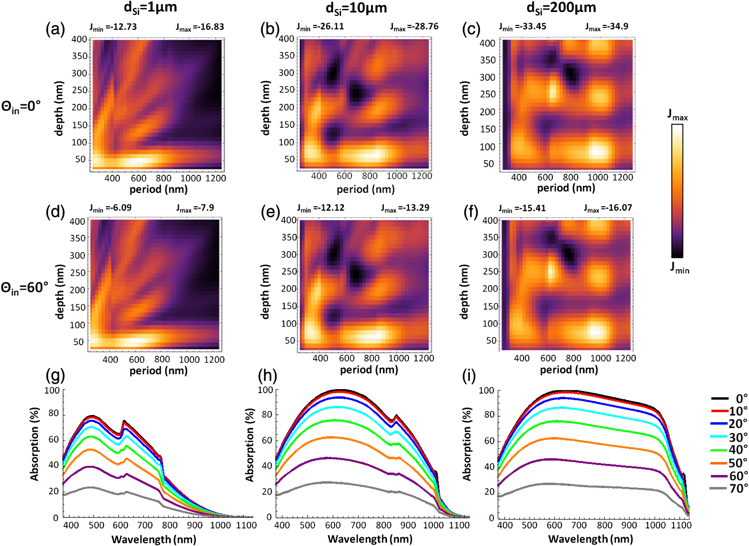 Figures 9(g)–9(i) show the absorption spectra of 1-, 10-, and 200-μm-thick silicon solar cells with optimized gratings for different angles of incidence starting from 0 deg up to 70 deg in steps of 10 deg. Figures 10(a)–10(c) plot the corresponding optimized photocurrent densities as a function of the angle of incidence. Since the incident sunlight flux passing through a unit surface area of a solar cell decreases with the cosine of the angle of incidence, the resulting photocurrent density should show a similar behavior. The thin green colored lines in Fig. 10 represent this limiting case given by Fig. 10(a)–(c) Maximum photocurrent densities (black dots) for 1, 10, and 200-μm-thick silicon solar cells as a function of the angle of incidence. The green curves indicate the photocurrent densities resulting from the values for normally incident light multiplied with the cosine of the angle of incidence. 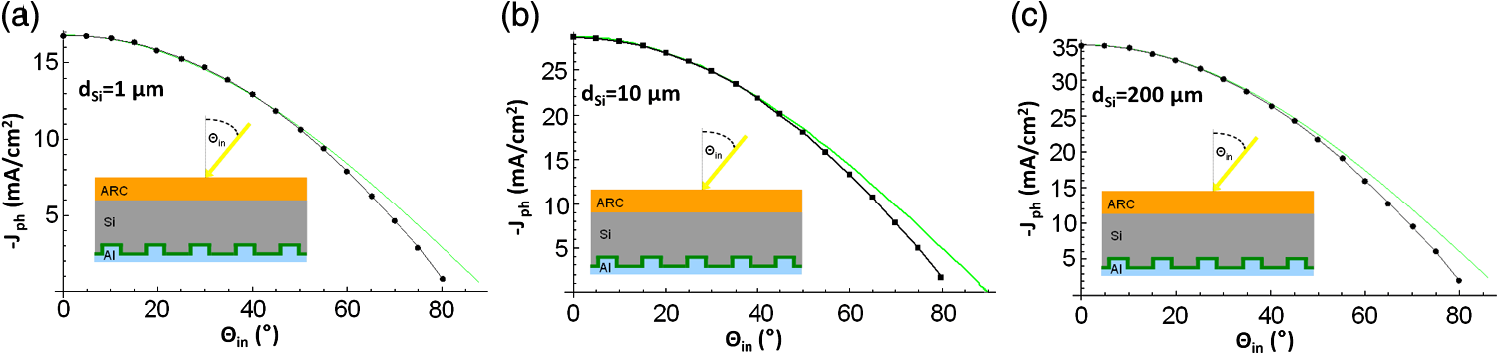 For angles the optimized photocurrent densities are in good agreement with this equation. For angles , the calculated photocurrent densities more and more deviate from this characteristic primarily due to the increase of front side reflection losses because the SiNx AR coating is optimized for normally incident light. 7.ConclusionIn this article, we employed a simulation approach that combines ray tracing with RCWA, which enables a strongly reduced computation time and a gain in simulation precision compared to fully electromagnetic simulation methods, such as RCWA or FDTD for solar cells thicker than . This approach also provided a much better physical insight into the light trapping mechanism of silicon solar cells with backside diffraction gratings. In contrast to fully electromagnetic simulation methods, characteristic humps in the absorption spectra can be observed that are directly related to the light trapping mechanism. We provided a detailed analysis and explanation for the origin of these characteristic humps in the absorption spectra, which helps in understanding the underlying light trapping mechanism in silicon solar cells with backside diffraction gratings. In addition, in this article, an in-depth analysis of the influence of the two determinant simulation parameters—the recursion depth and the diffraction order—on the simulation results was investigated. The results showed that for the optimum diffraction grating design, the proper choice of the recursion depth is of significant importance. Dependent on the silicon thickness the recursion depth must exceed a certain minimum value. While for 200-μm-thick solar cells at least two backside reflections/diffractions, i.e., must be taken into account, for 1-μm-thin cells a recursion depth of is necessary. Therefore, simulations taking into account only the first backside diffraction ( ) result in wrongly optimized grating parameters with significantly shorter periods, which do not fully exploit the light trapping effect and, thus, have a lower photocurrent density improvement. A recursion depth of turned out to be the best trade-off between simulation time and precision of the calculated photocurrent densities, for all investigated cell thicknesses ranging from 1 to 200 μm. With respect to the diffraction order, the analysis indicates that for silicon solar cells an inclusion of diffraction orders up to is sufficient to obtain correct simulation results. Furthermore, in this article, for the first time to the best of our knowledge, it was shown that the angle of incidence does not influence the optimum diffraction grating parameters for a given silicon thickness. Therefore, the optimization of silicon solar cells with backside diffraction gratings and planar front side AR coatings can be performed for normal light incidence. AcknowledgmentsThis work was supported by the Austrian NANO Initiative under the grant PLATON Si solar (project no. 819660). References
P. Sheng
A. N. Bloch
R. S. Stepleman
,
“Wavelength-selective absorption enhancement in thin-film solar cells,”
Appl. Phys. Lett., 43
(6), 579
–581
(1983). http://dx.doi.org/10.1063/1.94432 0003-6951 Google Scholar
C. Heine
R. H. Morf
,
“Submicrometer gratings for solar energy applications,”
Appl. Opt., 34
(14), 2476
–2482
(1995). http://dx.doi.org/10.1364/AO.34.002476 0003-6935 Google Scholar
S. H. Zaidi
J. M. Gee
D. S. Ruby
,
“Diffraction grating structures in solar cells,”
in 28th IEEE Photovoltaic Spec. Conf.,
395
–398
(2000). Google Scholar
P. Voisin
et al.
,
“Nanostructured back side silicon solar cells,”
in 24th European PV Solar Energy Conf. and Exhibition,
(2009). Google Scholar
R. Dewan
D. Knipp
,
“Light trapping in thin-film silicon solar cells with integrated diffraction grating,”
J. Appl. Phys., 106
(8), 074901
(2009). http://dx.doi.org/10.1063/1.3232236 0021-8979 Google Scholar
N. N. Feng
et al.
,
“Design of highly efficient light-trapping structures for thin-film crystalline silicon solar cells,”
IEEE Trans. Electron. Dev., 54
(8), 1926
–1933
(2007). http://dx.doi.org/10.1109/TED.2007.900976 0018-9383 Google Scholar
P. Bermel
et al.
,
“Improving thin-film crystalline silicon solar cell efficiencies with photonic crystals,”
Opt. Exp., 15
(25), 16986
–17000
(2007). http://dx.doi.org/10.1364/OE.15.016986 1094-4087 Google Scholar
L. Zeng
et al.
,
“Demonstration of enhanced absorption in thin film Si solar cells with textured photonic crystal back reflector,”
Appl. Phys. Lett., 93
(22), 221105
(2008). http://dx.doi.org/10.1063/1.3039787 0003-6951 Google Scholar
J. G. Mutitu
et al.
,
“Thin film solar cell design based on photonic crystal and diffractive grating structures,”
Opt. Exp., 16
(19), 15238
–15248
(2008). http://dx.doi.org/10.1364/OE.16.015238 1094-4087 Google Scholar
R. Rothemund
et al.
,
“Light trapping in monocrystalline Si solar cells using back-side diffraction gratings,”
Solid State Phenom., 178–179 446
–450
(2011). http://dx.doi.org/10.4028/www.scientific.net/SSP.178-179 1012-0394 Google Scholar
M. Wellenzohn
R. Hainberger
,
“Light trapping by backside diffraction gratings in silicon solar cells revisited,”
Opt. Exp., 20
(S1), A20
–A27
(2012). http://dx.doi.org/10.1364/OE.20.000A20 1094-4087 Google Scholar
M. Wellenzohn
R. Hainberger
,
“Optimization of silicon solar cells using backside diffraction gratings,”
in Renewable Energy, and the Environment,
(2011). Google Scholar
M. Wellenzohn
R. Hainberger
,
“A 2D numerical study of the photo current density enhancement in silicon solar cells with optimized backside gratings,”
in 37th IEEE Photovoltaic Spec. Conf.,
002963
–002967
(2011). Google Scholar
M. Born
E. Wolf
, Principles of Optics, 61
–66 7th ed.Cambridge University Press, New York
(1999). Google Scholar
M. A. Green
M. J. Keevers
,
“Optical properties of intrinsic silicon at 300 K,”
Prog. Photovolt. Res. Appl., 3
(3), 189
–192
(1995). http://dx.doi.org/10.1002/(ISSN)1099-159X 1062-7995 Google Scholar
A. D. Rakić
,
“Algorithm for the determination of intrinsic optical constants of metal films: application to aluminum,”
Appl. Opt., 34
(22), 4755
–4767
(1995). http://dx.doi.org/10.1364/AO.34.004755 0003-6935 Google Scholar
I. H. Malitson
,
“Interspecimen comparison of the refractive index of fused silica,”
J. Opt. Soc. Am., 55
(10), 1205
–1208
(1965). http://dx.doi.org/10.1364/JOSA.55.001205 0030-3941 Google Scholar
A. Donges
,
“The coherence length of black-body radiation,”
Eur. J. Phys., 19
(3), 245
–249
(1998). http://dx.doi.org/10.1088/0143-0807/19/3/006 0143-0807 Google Scholar
C. R. Wheeler
R. D. Ramsier
P. N. Henriksen
,
“An investigation of the temporal coherence length of light,”
Eur. J. Phys., 24
(4), 443
–450
(2003). http://dx.doi.org/10.1088/0143-0807/24/4/363 0143-0807 Google Scholar
G. R. Reider
, Photonik, Eine Einführung in die Grundlagen, 31 Springer-Verlag, Wien
(2004). Google Scholar
Biography Markus Wellenzohn was born in Zams (Tyrol), Austria. He received the Dipl.-Ing. degree in physics from the Vienna University of Technology, Austria, in 2008. Since 2007 he has been working as a Junior Scientist for the AIT Austrian Institute of Technology GmbH. His research activities have been mainly related to silicon nanophotonics, where he focused on the simulation and design of photonic crystal sensors for optical biosensing as well as on light management for photovoltaics.  Rainer Hainberger was born in Vienna, Austria. He received the Dipl.-Ing. degree in physics from the Vienna University of Technology, Austria, in 1995 and the PhD degree in electrical engineering from the University of Tokyo, Japan, in 2000. From 2000 to 2004 he was affiliated with Fujitsu Laboratories Ltd., Japan, where he was working on Raman amplification in WDM transmission systems and all-optical signal processing including topics such as 2R regeneration and highly nonlinear photonic crystal fibers. Since 2004 he has been working for the AIT Austrian Institute of Technology GmbH. His research activities have been mainly related to optical biosensing employing silicon and polymer photonic concepts. Apart from that he has also been involved in research projects related to light management for photovoltaics. |