|
|
1.IntroductionIII-V nitride material systems, which include AlN, GaN, InN, and their alloys, have been widely investigated due to their tunable energy bandgaps and application in light-emitting diodes (LEDs), laser diodes, and solar cells. 1 , 2 The bandgap of InGaN material systems covers emission wavelengths from the near-ultraviolet (UV) to green regions, which essentially includes the entire functional range of the solar spectrum. 3 – 5 To obtain a high conversion efficiency, most InGaN solar cells studies have been confined to the green region, requiring an indium content of about 15% to 30%. 6 – 9 The efficiency of InGaN solar cells having an emission wavelength in the green region is high due to the high In composition, compared with those under a green wavelength, though their fill factor (FF) remains low due to their perceived poor crystal quality. In the early days of InGaN-based solar cells, most research focused on p-i-n solar cells having an intrinsic InGaN layer. 10 – 13 However, it is difficult to fabricate the high-In composition and thick intrinsic InGaN layer required to increase the absorption due to the large lattice mismatch between InN and GaN. 14 Furthermore, the polarization effects in p-i-n structures adversely reduce internal electrical fields inside intrinsic InGaN layers, leading to a lower open-circuit voltage (Voc) and shorter circuit current (Jsc) compared with multiple quantum well (MQW) solar cells. 15 Accordingly, to maintain the high In composition and high crystal quality, several groups adopted InGaN/GaN MQW solar cells, 16 , 17 though these solar cells still have a low Jsc and FF. Also, other groups recently reported the carrier transport in InGaN/GaN solar cells by barrier thickness and temperature. 18 , 19 However, the carrier transport of InGaN/GaN solar cell by indium composition is not yet reported. In InGaN MQW structures having a high indium composition, carrier extraction also remains difficult due to the relatively high barrier height and strong piezoelectric field. The piezoelectric field is known to have an adverse effect on the tunneling rate, since it makes electrons and holes travel in opposite directions to which they contribute to the photocurrent. 20 In order to overcome the piezoelectric field, several methods have been studied. 21 – 24 Therefore, the further study of solar cells is essential in order to optimize InGaN solar cells requiring high efficiency. In this work, we investigate the properties of vertical-type solar cells (VSCs) having InGaN/(Al)GaN MQWs in terms of carrier transport, based on bias-dependent external quantum efficiency (EQE) measurements. To understand carrier transport in InGaN/(Al)GaN MQWs, we first fabricate VSCs that have emission wavelengths in the UV-blue-green regions. The conversion efficiency of these VSCs is subsequently found to be higher than for lateral-type solar cells due to a larger amount of light absorbed by the bottom reflector; 25 , 26 the textured n-GaN top surface is seen to absorb most of the light. These solar cell structures were grown using metal organic chemical vapor deposition (MOCVD), and all devices were fabricated using a conventional vertical LED process. 2.ExperimentsFigure 1(a) presents a schematic of the fabricated VSCs for UV, blue, and green wavelengths. InGaN-based VSCs having wavelengths of 385, 450, and 525 nm were grown on a c-plane sapphire substrate using MOCVD (Veeco D300 model, Gwangju, Korea). Figure 1(b) shows the scanning electron microscopy image of the top surface of the fabricated VSC. During growth, trimethylgallium, trimethylindium, and were used as precursors for Ga, In, and N, respectively. In addition, and were employed as the p- and n-type dopant precursors, and was used as the carrier gas for all growth periods, except for InGaN growth, where was used. The reactor pressure during growth was maintained at 200 Torr. The final structures consisted of a 2-μm-thick undoped GaN layer and a 4-μm-thick Si doped n-GaN layer. Then, for the UV-VSC, blue-VSC, and green-VSC, 7-period InGaN/(Al)GaN ( ) MQWs with 5%, 15%, and 28% indium composition were grown on the n-GaN ( ) layer, respectively, and aluminum composition in UV-VSC was 5%. The indium composition was subsequently confirmed using x-ray diffraction (not shown). Next, a 100-nm-thick Mg-doped p-GaN ( ) layer was grown on each MQW. All VSCs were fabricated as follows. All samples were sequentially cleaned in acidic and organic solutions to remove both native oxide and organic contamination. After cleaning, an Ni/Ag/Ni/Au layer was deposited on top of the p-GaN layer. Fig. 1(a) Schematic of fabricated VSC with InGaN MQW. (b) Scanning electron microscopy image of the top surface of fabricated VSC.  These multiple layers act as both a p-ohmic contact layer and a light-reflecting layer. A 2-μm-thick wafer-bonding Au/Sn layer was then deposited, and the wafer was subsequently bonded onto a bonding layer that was previously coated with a molybdenum conductive substrate using a thermocompressing bonding method at 300°C for 30 min. Next, using a KrF excimer laser at a wavelength of 248 nm, a laser lift-off process was used to separate the sapphire substrate from the InGaN/GaN MQW solar cell structure. Using wet and dry etching processes, the air-exposed undoped GaN was then etched to expose the n-GaN layer; a square mesa of was defined by dry etching for the isolation. To texture the n-GaN surface, 5 M dissolved potassium hydroxide (KOH) was used at 60°C for 30 min. Finally, a Cr/Au layer was deposited onto the textured n-GaN surface as an n-type contact electrode. The performances of fabricated VSCs were measured using the solar simulator and the quantum efficiency tester. The solar simulator simulates the sun light spectrum with the help of a Xe arc lamp, whose spectra match with that of the sun. Also, quantum efficiency tester is an instrument that gives the performance of the solar cell for different light intensities. A light of different wavelengths is generated from a polychromatic source (Xe arc lamp). 3.Results and DiscussionFigure 2 shows the current density relative to voltage (J-V) characteristics measured under darkened conditions and AM 1.5 G light illumination using a solar simulator. For the UV-VSC, blue-VSC, and green-VSC, Voc of 2.4, 2.2, and 2.0 V, respectively, were obtained. The differences in Voc could be attributed to the difference of indium composition among the samples; there were also differences in the Jsc and FF. The Jsc and the FF of the UV-VSC, blue-VSC, and green-VSC were and 73%, and 48%, and and 36%, respectively. The performance parameters of fabricated devices are summarized in Table 1. Fig. 2(a) J-V characteristics measured under dark and light illumination conditions. (b) Enlarged J-V curve ranging from 0 to 3 V. 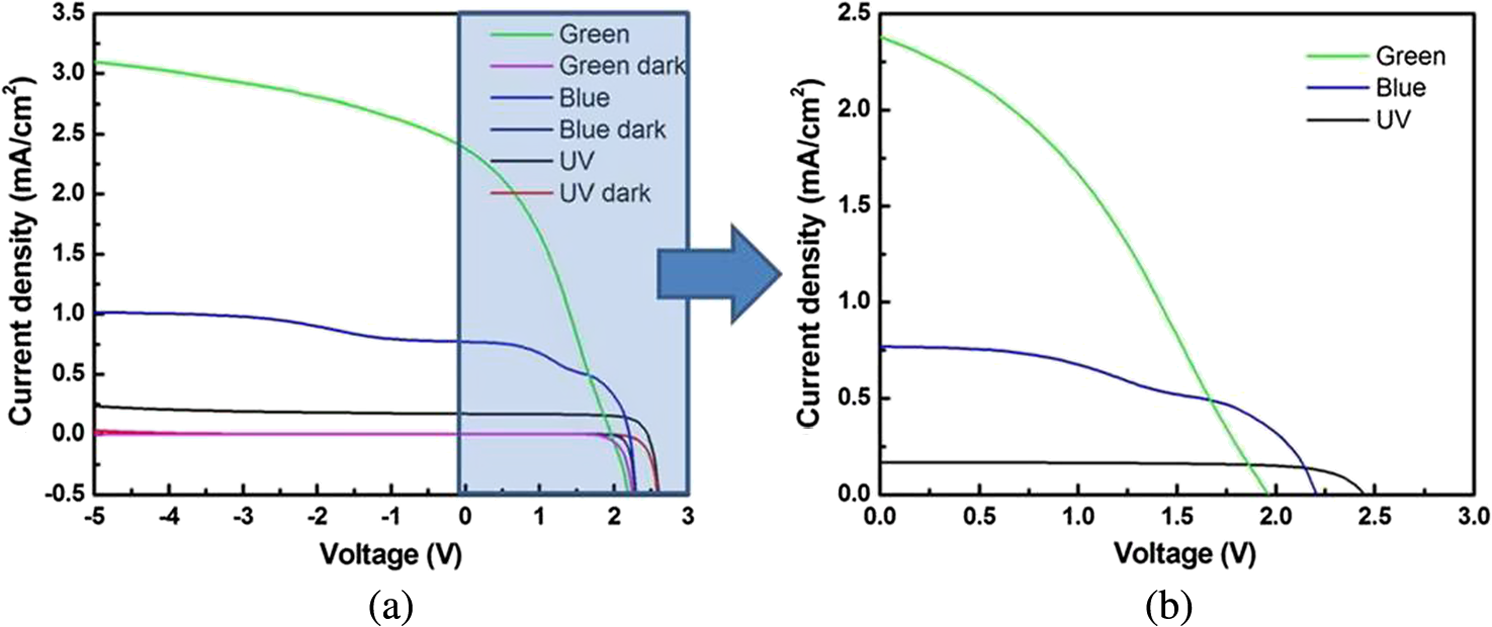 Table 1Performance parameters for fabricated devices.
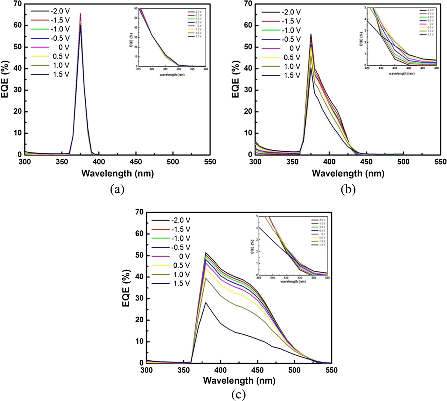
The difference in Jsc of the three samples could be explained by the overlapping EQE region of each sample with the solar spectrum, as shown in Fig. 3. Fig. 3EQE measurements of UV-VSC, blue-VSC, and green-VSC. The shaded area denotes the solar spectrum. 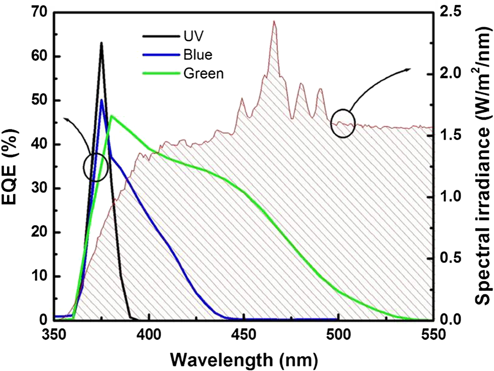 Figure 3 shows the EQE measurements of the UV-VSC, blue-VSC, and green-VSC with respect to the solar spectrum as a function of the wavelength; the peak EQEs were 63%, 50%, and 46%, respectively. It is posited here that this difference in the peak EQE can be attributed to the difference of barrier height due to indium composition. For instance, the EQEs of all VSCs rapidly decreased below , which is the bandgap of GaN. The reason for this abrupt EQE decrease in all VSCs is due to the stronger absorption through the thicker top n-GaN layer (about 4 μm). 19 The absorption wavelength limits of the UV-VSC, blue-VSC, and green-VSC were about 390, 450, and 550 nm, respectively, which correspond to their bandgap. In other words, the major light absorption of UV-VSC, blue-VSC, and green-VSC occurs in 360 to 385 nm, 360 to 450 nm, and 360 to 550 nm wavelength regions, respectively. Therefore, the Jsc of the green-VSC is the highest due to its broad overlapping region with the solar spectrum. To further understand the carrier transport from the UV-VSC, blue-VSC, and green-VSC, bias-dependent EQE measurements were performed at bias voltages ranging from to (Fig. 4). For the UV-VSC in Fig. 4(a), the bias-dependent EQE is similar under both a reverse and forward biases, i.e., carrier escape is easier than for other VSCs using a tunneling process from quantum wells due to the lower barrier height because of the low indium composition (about 5%). This result is in a good agreement with the J-V curve of UV-VSC, as shown in Fig. 2. The current density of UV-VSC shows little change under either a reverse or forward bias. Although the UV-VSC has a low Jsc ( ) due to its small absorption range (about 360 to 390 nm), its FF remains high due to the easy carrier transport by tunneling through the low barrier height, again originating from the lowindium composition. Figures 4(b) and 4(c) show the bias-dependent EQEs of the blue-VSC (indium composition: 15%) and green-VSC (indium composition: 28%), respectively. For these VSCs, the carrier in the QW was extracted via tunneling induced by energy-band bending as the reverse bias was increased, thereby increasing the carrier collection. However, when increased toward a forward bias, the EQEs of the blue-VSC and green-VSC decreased because the carrier escape probability was reduced due to the high-barrier height and strong piezoelectric field, indicating that the tunneling rate of the carrier was reduced and that the carrier was confined or recombined in the MQW. In particular, the EQE of the green-VSC more rapidly decreased than for the blue-VSC as the forward bias was increased due to the fact that the barrier height and piezoelectric field for the green-VSC were higher than for the blue-VSC due to its higher indium composition. In addition, this decrease caused an abrupt reduction in the Jsc for the green-VSC under a forward voltage (Fig. 2). In this work, piezoelectric field of the green-VSC and blue-VSC was and , respectively. The green-VSC has a larger piezoelectric field due to large lattice mismatch via higher indium composition. As such, the green-VSC displays a high Jsc due to its wider absorption range, while maintaining a low FF because of the low tunneling rate induced by carrier confinement or recombination. We confirmed here that the low FF of the green-VSC was due to a high-barrier height and strong piezoelectric field—caused by high indium composition—through bias-dependent EQE measurements. The insets of Figs. 4(a)–4(c) show the enlarged tail of each EQE curve near their absorption limit wavelength. From these curves, the value of the forward bias EQEs is seen to be higher than for the reverse bias EQEs, as the bandgap of InGaN-based MQWs is reduced due to the quantum confined Stark effect induced by a piezoelectric field under a forward bias, indicating that the absorption wavelength became red-shifted to a longer wavelength. As a result, we could obtain an optimum structure by maintaining a high indium composition for smoother carrier transport via a reduction in the barrier height such as in the InGaN/InGaN MQWs. 4.ConclusionWe fabricated InGaN-based VSCs having varying wavelengths of UV, blue, and green regions in order to investigate carrier transport as a function of indium composition via bias-dependent EQE measurements. With its high indium composition, the green-VSC had the highest Jsc and the lowest FF due to the reduction of the carrier tunneling rate based on its high barrier height and strong piezoelectric field. References
S. Nakamura
et al.
,
“Ridge-geometry InGaN multi-quantum-well-structure laser diodes,”
Appl. Phys. Lett., 69
(10), 1477
–1479
(1996). http://dx.doi.org/10.1063/1.116913 0003-6951 Google Scholar
T. Kozaki
S. Nagahama
T. Mukai
,
“Recent progress of high-power GaN-based laser diodes,”
Proc. SPIE, 6485 648503
(2007). http://dx.doi.org/10.1117/12.714208 0277-786X Google Scholar
J. Wu
et al.
,
“Small band gap bowing in
alloys,”
Appl. Phys. Lett., 80
(25), 4741
–4743
(2002). http://dx.doi.org/10.1063/1.1489481 0003-6951 Google Scholar
K. Y. Lai
et al.
,
“Effect of indium fluctuation on the photovoltaic characteristics of InGaN/GaN multiple quantum well solar cells,”
Appl. Phys. Lett., 96
(8), 081103
(2010). http://dx.doi.org/10.1063/1.3327331 0003-6951 Google Scholar
K. Y. Lai
et al.
,
“Origin of hot carriers in InGaN-based quantum-well solar cells,”
IEEE Electron Device Lett., 32
(2), 179
–181
(2011). http://dx.doi.org/10.1109/LED.2010.2091619 0741-3106 Google Scholar
O. Jani
et al.
,
“Design and characterization of GaN/InGaN solar cells,”
Appl. Phys. Lett., 91
(13), 132117
(2007). http://dx.doi.org/10.1063/1.2793180 0003-6951 Google Scholar
X. Chen
et al.
,
“Growth, fabrication, and characterization of InGaN solar cells,”
Phys. Stat. Sol. (A), 205
(5), 1103
–1105
(2008). http://dx.doi.org/10.1002/pssa.v205:5 0031-8965 Google Scholar
C. J. Neufeld
et al.
,
“High quantum efficiency InGaN/GaN solar cells with 2.95 eV band gap,”
Appl. Phys. Lett., 93
(14), 143502
(2008). http://dx.doi.org/10.1063/1.2988894 0003-6951 Google Scholar
X. Zheng
et al.
,
“High-quality InGaN/GaN heterojunctions and their photovoltaic effects,”
Appl. Phys. Lett., 93
(26), 261108
(2008). http://dx.doi.org/10.1063/1.3056628 0003-6951 Google Scholar
S. Zeng
X. Cai
B. Zhang
,
“Demonstration and study of photovoltaic performances of InGaN p-i-n homojunction solar cells,”
IEEE J. Quantum Electron., 46
(5), 783
–787
(2010). http://dx.doi.org/10.1109/JQE.2009.2039197 0018-9197 Google Scholar
J. P. Shim
et al.
,
“Improved efficiency by using transparent contact layers in InGaN-based p-i-n solar cells,”
IEEE Electron Device Lett., 31
(10), 1140
–1142
(2010). http://dx.doi.org/10.1109/LED.2010.2058087 0741-3106 Google Scholar
R. H. Horng
et al.
,
“Improved conversion efficiency of textured InGaN solar cells with interdigitated imbedded electrodes,”
IEEE Electron Device Lett., 31
(6), 585
–587
(2010). http://dx.doi.org/10.1109/LED.2010.2046615 0741-3106 Google Scholar
E. Matioli
et al.
,
“High internal and external quantum efficiency InGaN/GaN solar cells,”
Appl. Phys. Lett., 98
(2), 021102
(2011). http://dx.doi.org/10.1063/1.3540501 0003-6951 Google Scholar
I. Ho
G. B. Stringfellow
,
“Solid phase immiscibility in GaInN,”
Appl. Phys. Lett., 69
(18), 2701
–2703
(1996). http://dx.doi.org/10.1063/1.117683 0003-6951 Google Scholar
G. Namkoong
et al.
,
“Effect of III-nitride polarization on VOC in p-i-n and MQW solar cells,”
Phys. Status Solidi: Rapid Res. Lett., 5
(2), 86
–88
(2011). http://dx.doi.org/10.1002/pssr.201004512 1862-6254 Google Scholar
K.-T. Chen
et al.
,
“InGaN light emitting solar cells with a roughened N-face GaN surface through a laser decomposition process,”
Opt. Express, 18
(22), 23406
–23412
(2010). http://dx.doi.org/10.1364/OE.18.023406 1094-4087 Google Scholar
R. Dahal
et al.
,
“InGaN/GaN multiple quantum well concentrator solar cells,”
Appl. Phys. Lett., 97
(7), 073115
(2010). http://dx.doi.org/10.1063/1.3481424 0003-6951 Google Scholar
J. R. Lang
et al.
,
“Carrier escape mechanism dependence on barrier thickness and temperature in InGaN quantum well solar cells,”
Appl. Phys. Lett., 101
(18), 181105
(2012). http://dx.doi.org/10.1063/1.4765068 0003-6951 Google Scholar
J. J. Wierer Jr.
D. D. Koleske
S. R. Lee
,
“Influence of barrier thickness on the performance of InGaN/GaN multiple quantum well solar cells,”
Appl. Phys. Lett., 100
(11), 111119
(2012). http://dx.doi.org/10.1063/1.3695170 0003-6951 Google Scholar
J.-H. Song
et al.
,
“Role of photovoltaic effects on characterizing emission properties of InGaN/GaN light emitting diodes,”
Appl. Phys. Lett., 95
(26), 263503
(2009). http://dx.doi.org/10.1063/1.3272679 0003-6951 Google Scholar
D. F. Feezell
et al.
,
“Semipolar (20-2-1) InGaN/GaN light-emitting diodes for high-efficiency solid-state lighting,”
J. Disp. Technol., 9
(4), 190
–198
(2013). http://dx.doi.org/10.1109/JDT.2012.2227682 0193-2691 Google Scholar
H. Zhao
et al.
,
“Approaches for high internal quantum efficiency green InGaN light-emitting diodes with large overlap quantum wells,”
Opt. Express, 19
(S4), A991
–A1007
(2011). http://dx.doi.org/10.1364/OE.19.00A991 1094-4087 Google Scholar
R. A. Arif
Y.-K. Ee
N. Tansu
,
“Polarization engineering via staggered InGaN quantum wells for radiative efficiency enhancement of light emitting diodes,”
Appl. Phys. Lett., 91
(9), 091110
(2007). http://dx.doi.org/10.1063/1.2775334 0003-6951 Google Scholar
J. Zhang
N. Tansu
,
“Optical gain and laser characteristics of InGaN quantum wells on ternary InGaN substrates,”
IEEE Photonics J., 5
(2), 2600111
(2013). http://dx.doi.org/10.1109/JPHOT.2013.2247587 1943-0655 Google Scholar
R. H. Horng
et al.
,
“Improved conversion efficiency of GaN/InGaN thin-film solar cells,”
IEEE Electron Device Lett., 30
(7), 724
–726
(2009). http://dx.doi.org/10.1109/LED.2009.2021414 0741-3106 Google Scholar
S. Y. Bae
et al.
,
“Improved photovoltaic effects of a vertical-type InGaN/GaN multiple quantum well solar cell,”
Jpn. J. Appl. Phys., 50
(1), 092301
(2011). http://dx.doi.org/10.1143/JJAP.50.092301 0021-4922 Google Scholar
BiographySeung Hwan Kim received the BS, MS, and PhD degrees from Chonbuk National University, Jeonju, Republic of Korea, in 2006, 2009, 2013, respectively. Since 2013, he has been with Korea Photonics Technology Institute, as a researcher, where he worked on research about LEDs and solar cells. His current research involves GaN based vertical type LEDs, solar cells for high efficiency. Jae Phil Shim is a PhD candidate student in the School of Information and Communications at Gwangju Institute of Science & Technology (GIST) in the Republic of Korea under Prof. Dong-Seon Lee. He received his MS in optoelectronic device at GIST and his BS in electronic engineering at KyungHee University in 2011 and 2009, respectively. His current research involves GaN based light emitting diodes, solar cell and application of graphene for GaN based optoelectronic devices. Hyun Ho Park is a MS candidate student in the School of Semiconductor and Chemical Engineering at Chonbuk National University in the Republic of Korea under Prof. Gye Mo Yang. He received his BS at Chonbuk National University in 2012. His current research involves GaN based vertical type light emitting diodes using the nano sphere. Young Ho Song is a senior researcher in Korea Photonics Technology Institute (KOPTI) in the Republic of Korea. He received the BS, MS, and PhD degrees from Chonbuk National University, Jeonju, the Republic of Korea, in 1999, 2001, 2006, respectively. His research interests include the growth of laser diodes, LED, and visible light communication using GaN based optical devices. Hyung Jo Park is a senior researcher in Korea Photonics Technology Institute (KOPTI) in the Republic of Korea. He received the BS and MS degrees from Chonbuk National University, Jeonju, the Republic of Korea, in 2001 and 2003, respectively. His current research interests include the fabrication of vertical type light emitting diodes and application of carbon nanotubes for GaN based optoelectronic devices. Seong Ran Jeon is a principal researcher in Korea Photonics Technology Institute (KOPTI) in the Republic of Korea. She received the BS, MS and PhD degrees from Chonbuk National University, Jeonju, the Republic of Korea, in 1997, 1999, and 2005, respectively. Her research interests include the growth of green light emitting diodes, and ultraviolet light emitting diodes. Dong-Seon Lee is a professor at the School of Information and Communications at Gwangju Institute of Science & Technology (GIST) in the Republic of Korea. He received his PhD in electrical and computer engineering from the University of Cincinnati in 2002. He received his MSc and BSc in physics from Seoul National University in 1989 and 1987, respectively. His main research interests include GaN based light emitting diodes, solar energy, nano- and micro-structured materials, plasmonics, and hydrogen generation materials. Seung Hyeon Yang received the BS, MS, and PhD degrees from Chonbuk National University, Jeonju, Republic of Korea, in 1983, 1985, 1992, respectively. Since 2013, he has been with Chonbuk National University as a professor, where he worked on research and lectured. His research fields were in structure and materials engineering of civil engineering. He is a member of the Korea Society of Steel Construction, Korea Society of Civil Engineers and Korea Academia-industrial Cooperation Society. Gye Mo Yang received the BS, MS, and PhD degrees in physics from Seoul National University, Seoul, Republic of Korea, in 1987, 1989, 1993, respectively. Since 1996, he has been a professor in the Department of Semiconductor Science and Technology, Chonbuk National University, Jeonju in the Republic of Korea. His research interests include the LEDs and VCSELs. He is a member of the Korea Physical Society. |