|
|
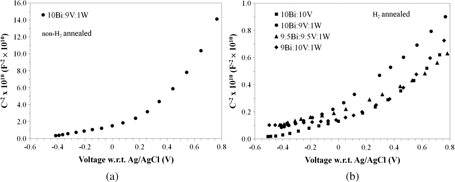
1.IntroductionIn , the Sun delivers more energy to Earth than the total worldwide primary energy consumption for an entire year. Capturing a small fraction of this energy would be a significant step toward meeting worldwide energy demands. A practical method for storage and transport of solar energy is by using a chemical energy carrier (fuel) such as hydrogen generated from sunlight. 1 – 3 For over 35 years, there has been interest in producing hydrogen from the sunlight powered photoelectrolysis of water in a photoelectrochemical (PEC) cell. The search for more efficient photocatalysts and methodologies to incorporate them into working devices is still an active area of research. 4 – 10 Such devices need to generate hydrogen with a solar-to-hydrogen efficiency of at least 10% (Refs. 8 and 11) and have a working lifetime of approximately 10 years. Commercial viability and widespread adoption of such solar-to-hydrogen fuel technologies necessitates low manufacturing costs. 1 , 9 , 10 Bismuth vanadate ( ) is a promising photoanode material for the oxidation of water into . 12 Low-cost and potentially scalable decomposition of bismuth and vanadium precursor solutions via spin coating, drop casting, and spray pyrolysis have produced monoclinic scheelite photoanodes. 13 – 15 The morphology of the produced films has been shown to affect the water oxidation performance of such photoanodes. 16 Increased electrode–electrolyte contact area may result in enhanced PEC performance. However, complex film morphologies that enhance surface area may also increase the number of surface states, defect sites, and grain boundaries, which can adversely affect charge separation and transport. 12 Hydrogen annealing treatments of films have been demonstrated to increase photoactivity, presumably resulting from oxygen vacancies in the treated films acting as shallow electron donors. 15 , 17 Tungsten doping of films has also been demonstrated to improve the PEC performance since W substitutions on vanadium sites also act as shallow electron donors. 15 , 18 , 19 In this study, the repeatability of ultrasonic spray pyrolysis as a potentially low-cost and scalable thin film manufacturing method for the production of photoanodes was investigated. The effects of hydrogen annealing treatments and W doping of these films were also investigated. Ultrasonic spray pyrolysis of an aqueous solution containing bismuth nitrate and vanadium oxysulfate was demonstrated to produce films with a complex, microporous, high-surface-area morphology. It was hypothesized that combining the large-surface-area films with tungsten doping and/or a hydrogen reduction treatment would result in photoanodes exhibiting excellent PEC performance. Following deposition, all films were calcined at 500°C. Subsequently, annealing at 375°C in a 3% atmosphere produced films with much larger photocurrent densities under AM1.5 illumination conditions than those that did not receive the hydrogen treatment. However, tungsten reduced the PEC performance of the photoanodes produced by this method. Although some of the undoped photoanodes produced state-of-the-art photocurrent densities at low bias, significant sample-to-sample variability in the films produced using this spray deposition process and the resulting PEC performance was observed. 2.Methodology2.1.Film Preparation and CharacterizationThin films of were fabricated by ultrasonic spray deposition of an aqueous precursor solution containing Bi, V, and W. The bismuth source was a solution of 0.04 M (99.999%, Alfa Aesar, Ward Hill, Massachusetts) in 0.5 M (Fisher Scientific, Waltham, Massachusetts). A solution of 0.04 M (99.9%, Sigma-Aldrich, St. Louis, Missouri) in 0.5 M was prepared as the vanadium source. Two different tungsten-containing solutions were used in this study. A 0.04 M in W solution was prepared by dissolving silicotungstic acid (STA), (certified, Fisher Scientific, Waltham, Massachusetts), in 0.5 M . A second 0.04 M in W precursor solution was prepared from (99.9%, Inframat Advanced Materials, Manchester, Connecticut) in 0.5 M . These solutions were then combined in different volumetric ratios to obtain the desired Bi, V, and W contents of the deposited films. Undoped was prepared by mixing equal volumes of the bismuth- and vanadium-containing solutions. Tungsten doping was achieved by adding the STA or ammonium metatungstate (AMT) solution to the mixture. Samples with 5% tungsten doping (calculated as a percentage of the total metal content) were produced by spray depositing precursor solutions formed from three different source mixing ratios— , , and . Films containing 1% tungsten doping were created from a precursor containing a source mixing ratio of . The aqueous precursor solution was deposited on glass or indium tin oxide (ITO)-coated glass (Delta Technologies). For each deposition, three substrates of approximately were placed on a hot plate maintained at 420°C. The precursor solution was nebulized using a 1.7-MHz ultrasonic transducer, and the generated mist (or fog) was transported to a linear scanning spray nozzle using air as the carrier gas. The spray pyrolysis system is similar to that described by Li et al. 15 except that in our system the nozzle motion is a simple back-and-forth translation. A deposition time of approximately 10 min was required to produce films of the desired film thickness. Once the desired film thickness was obtained, the air flow was stopped and the coated substrates were removed from the deposition apparatus and allowed to cool in air to room temperature. Following deposition, samples were annealed in air (calcined) at 500°C for 3 h to promote formation of the desired monoclinic scheelite phase. Some samples received a second annealing treatment at 375°C in a 3% atmosphere. Once annealed, samples for PEC testing were prepared by affixing a wire to the exposed ITO substrate using a two-part silver epoxy (Epoxy Technology EE129-4, Billerica, Massachusetts). Samples were then baked for 75 min at 97°C to cure the silver epoxy. Resistance measurements were performed to ensure conductivity between the conducting substrate and the wire. Finally, the wires and exposed conducting substrate were coated with clear insulating epoxy (2 Ton insulating epoxy, Devcon, Danvers, Massachusetts) resulting in photoanode samples with exposed surface areas ranging from 0.3 to . An Alpha-Step 500 surface profiler was used to measure the thickness of the resulting films. A LEO 1430VP scanning electron microscope (SEM) with an Oxford energy dispersive x-ray spectrometer system (EDS) was used to analyze the film morphology and chemical composition. Power x-ray diffraction (PXRD) data were collected using Cu radiation on a PANalytical X’Pert PRO powder diffractometer equipped with an X’Celerator detector. Data were collected between 5 and 70 deg in scanning mode with a step size of 0.03 deg and a count time of 250 s. 2.2.PEC MeasurementsPEC measurements were performed in a three-electrode cell containing a 0.5 M (99.5%, Fisher Scientific) electrolyte with a phosphate buffer (pH at 25°C, Micro Essentials Laboratory, Brooklyn, New York). The photoanodes served as the working electrodes. A 4-M KCl electrode (Accumet, Fisher Scientific) was used as the reference electrode and a platinum mesh served as the counter electrode. Potential measurements are reported with respect to the reference electrode. A Keithley 2400 SourceMeter configured as a potentiostat was used to perform linear sweep voltammetry at a sweep rate of . Voltammograms were obtained for samples illuminated by simulated solar radiation with an intensity of at the sample surface. The simulated solar illumination was produced with an Oriel 96000, 150-W solar simulator (Newport) with an AM1.5 filter. Photocurrent data with both frontside illumination and through-substrate illumination conditions were collected and compared to dark current measurements. To compare the PEC performance of the different size photoanode samples, the measured current was divided by the area exposed to the electrolyte solution to obtain the photocurrent density, . 3.Results3.1.Film Morphology and StructureAs deposited, undoped samples created from the bismuth and vanadium precursors exhibited the characteristic yellow color of . Samples prepared with precursors containing 1% and 5% (atomic percentage) tungsten were yellow-orange. Following calcining at 500°C, all of the deposited films, including the W-containing films, had an opaque yellow color. Samples that received the subsequent annealing in 3% did not exhibit a significant difference in appearance. Visible and optical microscope examination of the tungsten-doped films revealed irregularities in the film roughness across the sample area. More specifically, some areas of the films appeared rough and nonreflective while others were smoother and more reflective. Such irregularities were far less evident for undoped samples. Streaking, indicative of thickness variations due to small irregularities in the spray nozzle flow pattern, was also observed on all of the samples. The resulting films exhibited a unique microstructure, as seen in the representative SEM images in Fig. 1. Figure 1(a) shows an undoped, calcined, and -annealed sample. A high-surface-area coral-like structure comprising connected hollow spheres and spherical fragments was evident. This most likely resulted from the rapid drying and decomposition of the ultrasonically nebulized precursor droplets and is similar to particle architectures observed by Dunkle et al. 20 Surface profile measurements indicated average film thicknesses between 1.7 and 2.2 μm with significant variations due to the complex morphology shown in the SEM images in Fig. 1. Fig. 1Scanning electron microscope images of the films created from precursor ratios of (a) , (b) , (c) , and (d) . The tungsten source for all of the films shown was silicotungstic acid (STA). Arrows in (d) indicate rod-like structures in the film. The scale bar shown represents a 5.0-μm length. 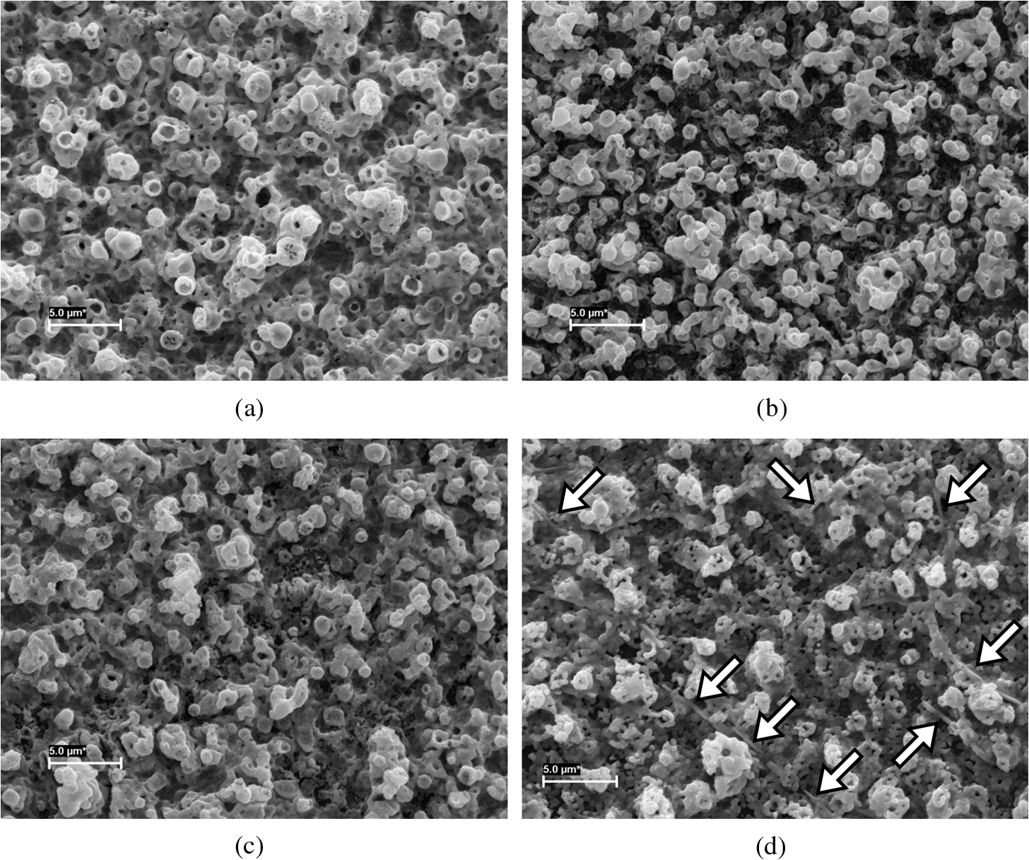 Figures 1(b)–1(d) show representative SEM images of calcined and treated films doped with 5% (atomic percentage) W from precursor ratios of (b) , (c) , and (d) using STA as the tungsten source. No morphology changes attributable to calcining or annealing were detected. Although all of the deposited films exhibited similar morphologies, small variations in the W-doped films were observed. In general, tungsten-doped films exhibited fewer and smaller hollow partial sphere structures compared to undoped samples. The most significant morphology difference was observed in Fig. 1(d), where small rod-like structures, indicated with arrows, were present throughout the film. SEM studies of all of the films indicated that such rod-like structures were present near the edges of W-doped films where spray coverage was minimal and the film was sparse. However, these structures were not found in the more complete coverage areas of films prepared from the and precursor solutions, suggesting that this morphology is unique to the vanadium-rich composition and forms when vanadium is in excess. EDS measurements of the film compositions indicated a close relationship between the precursor composition and the atomic percentage composition of the films produced. Spectral analysis of the rod-like structures observed in Fig. 1(d) confirmed that they were vanadium and tungsten rich. PXRD measurements of undoped samples deposited on glass, shown in Fig. 2, indicated that after calcining the films likely comprised monoclinic scheelite (PDF#14-0688). PXRD pattern (a) of an as-deposited film prior to calcining suggested a scheelite tetragonal structure (PDF#75-2481) and showed the presence of unidentified phases. This indicates that while the solution delivered the components to the film, they do not react completely during the deposition process. Following annealing in air at 500°C, the PXRD patterns of undoped films, such as the one shown in pattern (b), matched the monoclinic scheelite phase, showing that annealing is required to facilitate the reaction and produce of the desired phase. Pattern (c) was obtained from an undoped film following the reducing treatment. No significant changes were observed in the PXRD patterns of undoped films that received the 3% annealing treatment, suggesting that the treatment did not significantly alter the film structure or composition. Samples with low levels of doping, such as shown in pattern (d), maintain the monoclinic scheelite structure. Fig. 2PXRD patterns of thin films samples from a (equimolar) precursor (a) as deposited, (b) calcined at 500°C, and (c) following annealing. Patterns (a)–(c) were collected on the same sample. PXRD patterns of W-doped films that were calcined and annealed following spray deposition with precursor mole ratios of (d) (AMT), (e) (STA), (f) (STA), and (g) (STA). 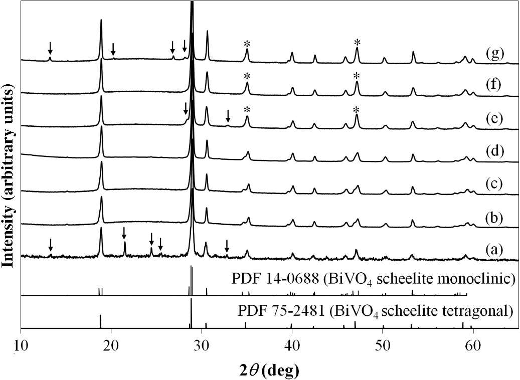 Increasing the amount of tungsten doping on the vanadium site causes the material to crystallize in the tetragonal scheelite structure (PDF#75-2481), 21 , 22 which is closely related to the structure of monoclinic scheelite. The scheelite phase ( ) contains an eight-coordinate cubic site (A site) and a four-coordinate tetrahedral site (M site). Previous work shows that hexavalent ions such as and dope exclusively on the M site, 21 , 22 and in the process create a vacancy on the A site to maintain charge balance. This is consistent with ionic radii: four-coordinate (49.5 pm) and (56 pm) have much smaller radii than eight-coordinate (131 pm). 23 Increasing the amount of substitution on the M site causes the material to undergo the monoclinic to tetragonal distortion. This distortion is not seen for low amounts of substitution, but is observed for larger amounts of substitution. Sleight et al. observe this transformation at for ( ), a 30% substitution. In the same work, they show that doping on the A-site does not produce this distortion. 22 The shape of the peaks near 35 and 47 deg can be used to distinguish between the monoclinic and tetragonal phases of . Tetragonal has a single (020) reflection near 35 deg; a change to the lower-symmetry monoclinic crystal system causes this peak to separate into two distinct reflections: (200) and (020). Similarly, at 47 deg , the (024) reflection for the tetragonal cell splits into three distinct reflections: (060), (240), and (042). The film in pattern (e) was obtained from a calcined and annealed film deposited with a precursor composition ratio of using STA as the tungsten source. In pattern (e), two impurity peaks were observed at 28 and 32.5 deg . More importantly, the single peaks observed near 35 and 47 deg (marked with asterisks), indicate the presence of tetragonal scheelite phase. The 10% doping on the V site ( ) is a lower doping level than thought necessary to produce this distortion. Since processing conditions are known to affect the amount of doping in these materials, 24 , 25 it would not be surprising if they also affected the underlying structure. Excess Bi should be observed in this film. However, it is common for impurity phases that are of the film not to be observed in PXRD data, or the excess Bi could be in an amorphous phase or in the unidentified impurity peaks. The peak shapes from pattern (f), obtained from a calcined and -annealed film deposited from a precursor composition ratio of using STA as the tungsten source, were consistent with a tetragonal cell. No additional peaks were observed, suggesting that the tungsten was incorporated in the host material or is present as an amorphous phase. Figures 3(a) and 3(b) show a detailed comparison of the reference and sample patterns (c), (d), and (f) near 35 and 47 deg , respectively, that were used to determine the crystalline phase compositions of the samples. The decrease in the number and the sharpening of the peaks as W is added indicates that the phase transition from the monoclinic to the tetragonal phase is easily seen in this figure. Allowing for broadening caused by the size of the crystallites, (c) matches the monoclinic pattern. Although (d) clearly shows the monoclinic structure, the difference in the peak shapes most likely results from the change in lattice parameters upon W doping. The presence of small amounts of the tetragonal phase in (d) or the monoclinic phase in (f) cannot be ruled out, and it is possible that these samples contained mixed phases. Even so, it is clear that the spray pyrolysis film changes from monoclinic to tetragonal as W is add to the precursor solution. Fig. 3PXRD patterns of samples (c), (d), and (f) from Fig. 2 near (a) 35 and (b) 47 deg compared to the reference patterns of the scheelite tetragonal (PDF#75-2481) and scheelite monoclinic (PDF#14-0688) phases. 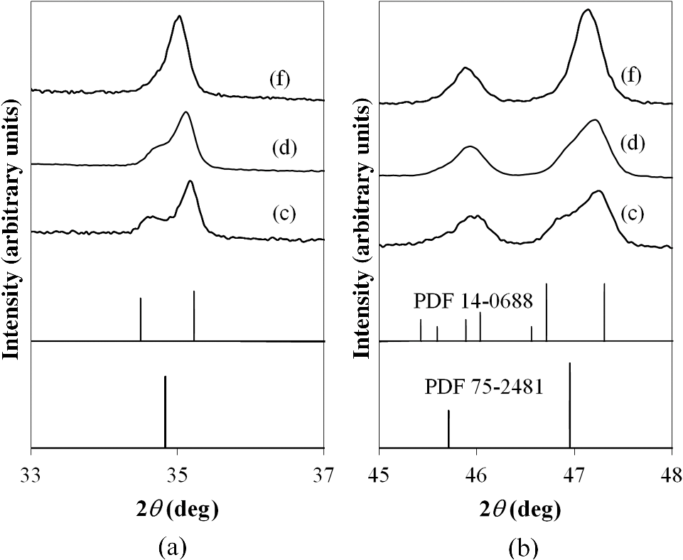 Finally, pattern (g) of Fig. 2 was obtained for a calcined and -annealed film deposited from a precursor composition ratio of using STA as the tungsten source. The peaks near 35 and 47 deg were determined to be consistent with the tetragonal phase. Additional peaks at 13, 20, 27, and 28 deg are observed. As with patterns (a) and (e), the additional peaks indicate the presence of an impurity phase that could not be fully explained by patterns in the database. These peaks may result from the rod-like structures observed in the SEM images. Based on the EDS analysis of the rod-like morphologies observed in Fig. 1(d) and the precursor composition, it is believed that these peaks may result from a phase or phases rich in vanadium and tungsten. This is consistent with the crystal chemistry of this system. Since tungsten cannot substitute on the bismuth site, and the combined V plus W content is well in excess of the amount of bismuth, they could crystallize as the impurity phase observed by PXRD. 3.2.PEC Study ResultsFigure 4 shows representative linear sweep voltammograms obtained for the photoanodes. Black lines represent the current density obtained when the sample was illuminated from the electrolyte interface (front) side. Gray lines indicate the current density obtained when the photoanode was illuminated through the substrate (back) side. Frontside and backside illumination studies were performed to provide insight into charge transport properties. 12 Voltammograms (a) and (b) were obtained from undoped, calcined, and -annealed photoanode samples created using the same precursor preparation and deposition procedures. Trace (c) shows the dark current density of the samples, illustrating that the current produced by samples (a) and (b) was from simulated solar light exposure. Sample (a) was one of the best-performing samples created using the described fabrication methods. It produced the largest frontside illumination photocurrent density of all samples tested in this study, particularly at low-bias voltage conditions. Sample (b) was more typical of the PEC response of undoped and treated samples, exhibiting a larger photocurrent when illuminated from the substrate side of the film at high-bias voltages. Fig. 4Linear sweep voltammograms of photoanodes with frontside (black) and backside (gray) illumination. Scans (a) and (b) were obtained from undoped, calcined, and annealed samples and (c) is the dark current scan. Scans (d)–(f) were obtained from W-doped, calcined, and annealed samples deposited from solutions of (d) , (e) , and (f) . AMT was the W source for these samples. Scan (g) shows the dark current measurements for samples (d)–(f). 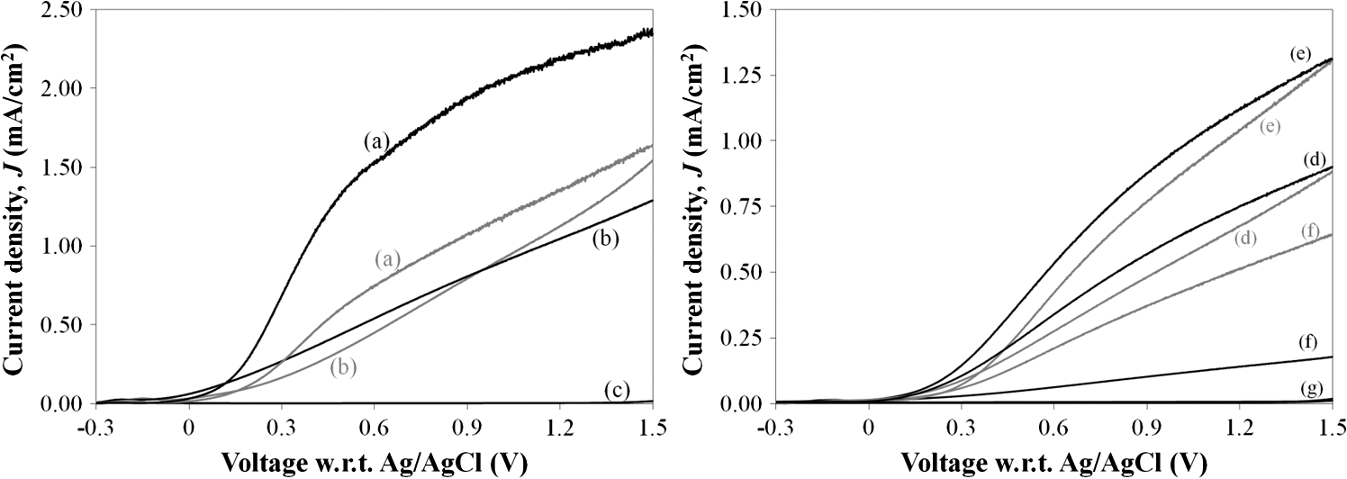 The remaining traces show example voltammograms obtained for 5% W-doped photoanodes that were calcined and annealed. AMT was used as the W source for these samples. Note the difference in the photocurrent density axis scale relative to that for plots (a)–(c). Curves (d), (e), and (f) were obtained from samples deposited from , , and precursor solutions, respectively. Plots (d) and (e) exhibited similar frontside and backside illumination responses, while sample (f) showed a significant photocurrent enhancement with backside illumination. Over 40 photoanode samples were fabricated during the course of this study to evaluate the repeatability of the ultrasonic spray deposition process to form photoanodes with consistent PEC performance. Figure 5 presents a comparison of the measured PEC performance for 27 of these samples. In Fig. 5, each bar represents the photocurrent density measured at three different bias voltages: 0.5 V (black bars), 1.0 V (dark gray bars), and 1.5 V (light gray bars) with respect to the reference electrode. Because the photocurrent density was measured for both frontside and backside illuminations, each sample is represented by a pair of bars. The bar on the left of each pair corresponds to the observed frontside illumination photocurrent while the bar on the right represents the measurements for substrate side illumination. Samples are grouped according to their composition, as indicated by the text above and below the bar groupings. The group of three samples at the right side of the graph, denoted 5% W, represent samples doped with 5% W from different precursor ratios that did not receive the treatment. The group of two undoped samples near the right side of the graph also did not receive the treatment. The parenthetical lower-case symbols denote the samples with voltammograms presented in Fig. 4. Finally, the upper case A and S above the sample bars denote AMT or STA, respectively, as the W source in the precursor solution. Fig. 5A comparison of the measured PEC performance of samples produced throughout the course of this study. Each pair of bars represents the photocurrent density measured under frontside (left) and substrate side (right) illumination conditions with 0.5-V (black bars), 1.0-V (dark gray bars), and 1.5-V (light gray bars) bias with respect to the reference electrode. Samples are grouped according to their composition and postdeposition treatment conditions. Parenthetical lowercase letters correspond to the voltammograms presented in Fig. 4. The uppercase A and S letters designate AMT and STA as the W doping source, respectively. 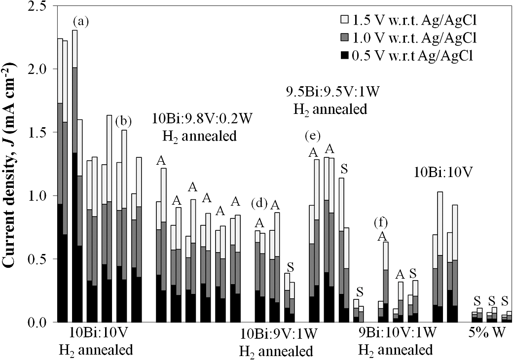 Note that Fig. 5 provides a summary of representative results obtained from the linear sweep voltammetry investigation of the samples. Multiple voltammograms were acquired for each photoanode sample nonsequentially over the course of several months to verify the repeatability of the measurements. Results from repeated voltammetry scans of the same sample showed repeatable PEC performance with little to no degradation of the test samples. The results presented in Fig. 5 clearly demonstrate that the hydrogen annealing treatment resulted in higher photocurrent production. Undoped samples that received the treatment produced, on average, the greatest photocurrent densities, as shown by the first group of bars in the chart. However, while two of the undoped and treated samples produced significant photocurrents at both low- and high-bias conditions, variability in the PEC performance of these samples is evident, even though all six of the undoped and treated samples were produced using the same precursor preparation and deposition techniques. The results presented in Fig. 5 also show that 5% tungsten doping did not produce the expected enhancement in PEC performance. This result is especially evident when comparing the PEC results from the doped and undoped air annealed samples. Hydrogen annealing improved the performance of the W-doped samples. However, significant performance variability existed between the different precursor combinations and within the duplicate samples. Of the 5% W-doped and -treated samples, those produced from a precursor composition containing provided the greatest photocurrent densities. Even in this case, tungsten doping produced no improvement over the undoped, -annealed photoanodes. Significant performance variability between samples produced with this composition is evident, particularly for films where STA was used as the W source. Also of note is the difference in photocurrent production between frontside and backside illuminations. With the exception of photoanodes produced from the and , the frontside illumination photocurrent density was larger than the backside illumination photocurrent density at low-bias conditions. This suggests that at low bias the PEC performance was limited by low hole mobility. However, at high bias, many of these samples exhibited improved backside illumination photocurrent densities, suggesting that the high electric field improved hole transport and that frontside high-bias performance was limited by poor electron transport through the film. The photocurrent onset potentials for the undoped photoanode samples under frontside illumination ranged from to for both samples that received the treatment and those that did not. Similarly, all 5% W-doped samples, irrespective of treatment, exhibited photocurrent onset potentials under frontside illumination ranging from to . The backside illumination photocurrent onset potentials exhibited similar behavior but with a slight (5 to 10 mV) increase in the potential. This increase is presumed to be due to reflection and absorption losses in the glass and ITO substrate. In an attempt to better quantify the flat-band potentials of the photoanodes, a Mott-Schottky analysis was explored. Figure 6 shows the Mott-Schottky plots obtained by measuring the capacitance of the film at different bias voltages with respect to the reference electrode when immersed in a 0.5-M electrolyte with no illumination. A 1000 Hz, 10-mV sinusoidal perturbation of the bias voltage was used to measure the film capacitance measurements. Figure 6(a) shows the resulting Mott-Schottky plot for a sample deposited from a precursor ratio that was only calcined. Figure 6(b) shows the same plot for an undoped sample and three W-doped samples that were calcined and annealed in . Note the difference in the scale for figures (a) and (b). The resulting data exhibited nearly continuous curvature with no well-defined linear region. Although not shown here, the Mott-Schottky measurements also exhibited frequency dependence, resulting in different functionalities when tested with a 500- and 200-Hz perturbation. This is believed to result from the nondense, highly microporous morphology of the films. 11 Because of this, conclusive flat-band potential estimates could not be ascertained. Visual inspection of the resulting plots suggests that the W-doped samples, irrespective of treatment, may have a more negative flat-band potential, consistent with the photocurrent onset potential measurements. Qualitative information about the carrier densities in the films could be evaluated. The Mott-Schottky measurements for the annealed samples in Fig. 6(b) exhibited a significantly reduced slope when compared to that of the non- annealed sample in Fig. 6(a), suggesting greater carrier concentrations in the annealed samples. 4.AnalysisBased on the PEC performance of the photoanodes produced in this study, it is evident that undoped films that were annealed in a 3% atmosphere exhibited the most desirable photocurrent characteristics, consistent with the findings of Wang et al. 17 The undoped treated films show a factor of improvement in the photocurrent densities compared to the undoped non- treated films. This increased performance is most likely results from the formation of oxygen vacancies within the film, which act as shallow electron donors, which increase the photoactivity and conductivity of the films. 19 The carrier concentration enhancement due to the annealing treatment was evident in the Mott-Schottky measurements. Although two of the undoped, treated samples exhibited excellent photocurrent generation at low-bias conditions, comparatively reduced performance was observed for four other undoped and annealed samples produced using the same method. This variability is assumed to be caused by slight differences in morphology and composition of the ultrasonically spray deposited films and shows the challenges that must be overcome before large-scale manufacturing of these photoelectrodes could occur. Although the enhanced surface area of the microporous films provides numerous sites for photoxidation, photogenerated electrons must be transported through restricted paths in the complex film morphology to collect at the underlying ITO layer. Numerous grain boundaries along these conduction paths are expected to further impede electron transport. phase differences that are undetectable by the PXRD studies may exist at grain boundaries, particularly at the interfaces between the interconnected spheres of the film structure. Such interface phase differences could decrease the electron transport through the film. Limited electron transport through the material is suggested by the increased photocurrent production of some of the undoped films with substrate side illumination. When the film is illuminated near the conducting substrate, the path length for electron transport, and hence the number of defect sites potentially encountered following photoexcitation, is reduced, resulting in a photocurrent increase. The PEC performance of our best undoped and -annealed films was superior to other published results. In contrast to the results of the previous studies, 12 , 14 , 15 W doping of our films resulted in reduced PEC performance. Tungsten is expected to be a shallow electron donor in , particularly when W is substituted on a V site. 19 Photocurrent onset measurements of the films and qualitative analysis of the Mott-Schottky plots in Fig. 6 suggest that the W doping of the films decreased the flat band potential of the photoanodes, irrespective of the treatment. However, this decreased flat band potential, and associated band bending enhancement, did not translate into increased photocurrent generation. PXRD patterns of the W-doped films indicated the presence of phases in addition to the monoclinic scheelite phase. Further, SEM indicated slight modification of the spray-deposited film morphology when W was added. It is therefore assumed that the inclusion of tungsten into the microporous structure may have generated impurity phases within the film, which may have also altered the film morphology. Potentially, tungsten segregation and phase impurities may have collected at the grain boundaries and acted as carrier traps. Because this has not been observed by other groups studying more dense (i.e., less microporous) films, it is assumed that the PEC performance reduction associated with W doping is a result of the deposition process and resulting microporous morphology rather than the intrinsic properties of the material. Although W substitutions on V sites were expected to improve the PEC performance of the photoanodes, it was observed that films deposited from a precursor ratio, a ratio selected to encourage such substitutions, exhibited reduced photocurrent production relative to films deposited from a precursor ratio. Similarly, films produced from a precursor ratio exhibited decreased photocurrent productions relative to the samples. PXRD patterns clearly show the presence of unidentified phases in the and samples, while the PXRD pattern of the sample showed little evidence for impurity phases. Similarly, the SEM images suggest that the composition exhibited a morphology more closely related to the undoped samples than the other doping ratios. It is therefore surmised that the performance differences are due to a combination of phase impurities near grain boundaries and morphological differences promoted by the addition of tungsten. In the , this performance could also be related to the monoclinic to tetragonal change in the crystal system of the material. Among the 5% W-doped samples, it is interesting to note the difference in photocurrent production between frontside and substrate side illumination conditions. Photoelectrodes produced from the precursors showed similar front versus backside illumination photocurrent densities. This suggests that the surmised impurity phases were either well distributed throughout the film or reduced hole and electron transport in a similar manner. For the films, substrate side illumination resulted in significantly increased photocurrent production, suggesting that the impurities within the film reduced electron transport. 5.ConclusionsThin films of were deposited on glass and ITO-coated glass via ultrasonic spray pyrolysis using an aqueous precursor solution containing bismuth nitrate and vanadium oxysulfate. Liquid precursor droplets formed by the 1.7-MHz ultrasonic transducer rapidly dried and decomposed, forming a highly microporous morphology comprising connected hollow spheres and sphere fragments. Undoped films that received a -reducing treatment following deposition and calcining exhibited the best PEC performance of all films studied, presumably due to high surface area of the film and the formation of oxygen vacancies within the film from the reducing treatment. Furthermore, our best undoped films have photocurrent densities superior to undoped films reported by other groups. Although two of the -treated photoanodes produced 0.9 and of photocurrent at 0.5-V bias with respect to the reference electrode, significant PEC performance variability was observed with films deposited in the same manner. This result indicates that the ultrasonic spray deposition and subsequent annealing of as described can produce photoanodes suitable for photoelectrolysis but refinements are needed in order to develop a reliable process that can be scaled for production. Contrary to the results of prior studies, doping the porous films with W resulted in a decreased PEC performance. Hydrogen-annealed films deposited from a precursor solution containing atomic ratio exhibited the best PEC performance of the tungsten-doped samples, although the significant performance variability was again observed. Comparing -annealed and 5% W-doped samples formed with a to -treated and 1% W-doped samples formed from a composition indicated a slight PEC performance decrease in the 5% W-doped samples, suggesting that the inclusion of W in the films was the source of PEC performance reduction. This is also in the regime where the material changed from monoclinic to tetragonal scheelite phase. Samples formed with AMT as the W precursor did not show significant PEC performance differences from those deposited with STA in the precursor solution, indicating that the tungsten precursor selection did not significantly impact the results. Although the exact reasons for the reduction in PEC performance of the W-doped films are not fully known, it is suspected that it is due to a combination of crystal structure, morphology, and film composition differences. The PXRD patterns of the W-doped films suggested that the dopant addition in these microporous films encouraged the formation of unidentified phases within the films. Morphology differences were also observed in the W-doped films formed from different precursor atomic ratios. Such mixed phases within the film, particularly at the many grain boundaries of the porous film, may act as carrier recombination sites, effectively reducing the conductivity of the films and subsequently the photocurrent production. The observed morphology differences between the films may be an indication of the presence of different phases within the films. Furthermore, all tetragonal samples showed decreased PEC performance. In conclusion, it was demonstrated that the annealing of films enhanced the PEC performance. Introduction of W doping into the -annealed films resulted in a performance decrease, presumably due to morphological changes, crystal structure changes, and the introduction of additional carrier recombination sites within the film. Although the spray deposition method described resulted in some photoanodes with excellent PEC performance under low-bias conditions, repeatable depositions were not realized. Thus, further investigation into the repeatability of the deposition method and postdeposition treatments must be carried out to improve the PEC performance and reduce the formation of impurity phases within the film. Other researchers have demonstrated that W doping of films can increase PEC performance, contrary to the results presented here; therefore, additional studies into the effect of W doping on the morphology, composition, and impurity phase formation within microstructured films should be performed to identify the mechanisms responsible for the observed reductions in the photocurrent generation. AcknowledgmentsThe authors would like to acknowledge undergraduate student researchers Joel Groetsema, Bartlett Jones, and Lauren Phillips for their assistance with this study. We would also like to thank Dr. Lance Kearns for his assistance and discussions related to the SEM imaging and EDS measurements. Support for this research work and undergraduate student involvement was provided by the College of Integrated Science and Engineering and the Center for Materials Science at James Madison University. We thank the National Science Foundation for partial support of the purchase of the powder diffractometer (DMR-0315345). References
R. Abe
,
“Recent progress on photocatalytic and photoelectrochemical water splitting under visible light irradiation,”
J. Photochem. Photobiol. C, 11
(4), 179
–209
(2010). http://dx.doi.org/10.1016/j.jphotochemrev.2011.02.003 1389-5567 Google Scholar
C. G. Grimes
O. K. Varghese
, Light, Water, Hydrogen: The Solar Generation of Hydrogen by Water Photoelectrolysis, Springer, New York
(2008). http://dx.doi.org/10.1007/978-0-387-68238-9 Google Scholar
N. S. Lewis
D. G. Nocera
,
“Powering the planet: chemical challenges in solar energy utilization,”
Proc. Natl. Acad. Sci. U. S. A., 103
(43), 15729
–15735
(2006). http://dx.doi.org/10.1073/pnas.0603395103 0027-8424 Google Scholar
A. Fujishima
K. Honda
,
“Electrochemical photolysis of water at a semiconductor electrode,”
Nature, 238 37
–38
(1972). http://dx.doi.org/10.1038/238037a0 0028-0836 Google Scholar
J. Bard
M. A. Fox
,
“Artificial photosynthesis: solar splitting of water to hydrogen and oxygen,”
Acc. Chem. Res., 28
(3), 141
–145
(1995). http://dx.doi.org/10.1021/ar00051a007 0001-4842 Google Scholar
K. Rajeshwar
,
“Hydrogen generation at irradiated oxide semiconductor-solution interfaces,”
J. Appl. Electrochem., 37
(7), 765
–787
(2007). http://dx.doi.org/10.1007/s10800-007-9333-1 0021-891X Google Scholar
H. Tributsch
,
“Photovoltaic hydrogen generation,”
Int. J. Hydrogen Energy, 33
(21), 5911
–5930
(2008). http://dx.doi.org/10.1016/j.ijhydene.2008.08.017 0360-3199 Google Scholar
A. L. Stroyuk
et al.
,
“Semiconductor photocatalytic systems for the production of hydrogen by the action of visible light,”
Theor. Exp. Chem., 45
(4), 209
–233
(2009). http://dx.doi.org/10.1007/s11237-009-9095-4 0040-5760 Google Scholar
M. Kitano
M. Hara
,
“Photocatalytic cleavage of water,”
J. Mater. Chem., 20
(4), 627
–641
(2010). http://dx.doi.org/10.1039/b910180b 0959-9428 Google Scholar
K. Maeda
,
“Photocatalytic water splitting using semiconductor particles: history and recent developments,”
J. Photochem. Photobiol. C, 12
(4), 237
–268
(2011). http://dx.doi.org/10.1016/j.jphotochemrev.2011.07.001 1389-5567 Google Scholar
Z. Chen
et al.
,
“Accelerating materials development for photoelectrochemical hydrogen production: standards for methods, definitions, and reporting protocols,”
J. Mater. Res., 25
(1), 3
–16
(2010). http://dx.doi.org/10.1557/JMR.2010.0020 0884-2914 Google Scholar
Y. Park
K. McDonald
K. Choi
,
“Progress in bismuth vanadate photoanodes for use in solar water oxidation,”
Chem. Soc. Rev., 42
(6), 2321
–2337
(2013). http://dx.doi.org/10.1039/c2cs35260e 0306-0012 Google Scholar
K. Sayama
et al.
,
“Photoelectrochemical decomposition of water into H2 and O2 on porous BiVO4 thin-film electrodes under visible light and significant effect of Ag ion treatment,”
J. Phys. Chem. B, 110
(23), 11352
–11360
(2006). http://dx.doi.org/10.1021/jp057539+ 1520-6106 Google Scholar
H. Ye
et al.
,
“Rapid screening of BiVO4-based photocatalysts by scanning electrochemical microscopy (SECM) and studies of their photoelectrochemical properties,”
J. Phys. Chem. C., 114
(31), 13322
–13328
(2010). http://dx.doi.org/10.1021/jp104343b 1932-7447 Google Scholar
M. Li
L. Zhao
L. Guo
,
“Preparation and photoelectrochemical study of BiVO4 thin films deposited by ultrasonic spray pyrolysis,”
Int. J. Hydrogen Energy, 35
(13), 7127
–7133
(2010). http://dx.doi.org/10.1016/j.ijhydene.2010.02.026 0360-3199 Google Scholar
P. Berglund
et al.
,
“Photoelectrochemical oxidation of water using nanostructured BiVO4 films,”
J. Phys. Chem. C, 115
(9), 3794
–3802
(2011). http://dx.doi.org/10.1021/jp1109459 1932-7447 Google Scholar
G. Wang
et al.
,
“Computational and photoelectrochemical study of hydrogenated bismuth vanadate,”
J. Phys. Chem. C, 117
(21), 10957
–10964
(2013). http://dx.doi.org/10.1021/jp401972h 1932-7447 Google Scholar
H. Park
et al.
,
“Factors in the metal doping of BiVO4 for improved photoelectrocatalytic activity as studied by scanning electrochemical microscopy and first principles density-functional calculation,”
J. Phys. Chem. C, 115
(36), 17870
–17879
(2011). http://dx.doi.org/10.1021/jp204492r 1932-7447 Google Scholar
W. J. Yin
et al.
,
“Doping properties of monoclinic BiVO4 studied by first-principles density-functional theory,”
Phys. Rev. B, 83
(15), 155102
(2011). http://dx.doi.org/10.1103/PhysRevB.83.155102 0163-1829 Google Scholar
S. S. Dunkle
R. J. Helmich
K. S. Suslick
,
“BiVO4 as a visible-light photocatalyst prepared by ultrasonic spray pyrolysis,”
J. Phys. Chem. C, 113
(28), 11980
–11983
(2009). http://dx.doi.org/10.1021/jp903757x 1932-7447 Google Scholar
M. Cesari
et al.
,
“The crystal structures of the bismuth molybdovanadates and of the alpha-phase bismuth molybdate,”
J. Inorg. Nucl. Chem., 33
(10), 3595
–3597
(1971). http://dx.doi.org/10.1016/0022-1902(71)80688-7 0022-1902 Google Scholar
A. W. Sleight
K. Aykan
D. B. Rogers
,
“New nonstoichiometric molybdate, tungstate, and vanadate catalysts with the scheelite-type structure,”
J. Solid State Chem., 13
(3), 231
–236
(1975). http://dx.doi.org/10.1016/0022-4596(75)90124-3 0022-4596 Google Scholar
R. D. Shannon
C.T. Prewitt
,
“Revised values of effective ionic radii,”
Acta Crystallogr., Sect. B, 26
(7), 1046
–1048
(1970). http://dx.doi.org/10.1107/S0567740870003576 0567-7408 Google Scholar
W. Guo
et al.
,
“Phase content and particle morphology of Bi-Mo-V-O powders produced by aerosol pyrolysis,”
Mater. Res. Bull., 40
(8), 1371
–1387
(2005). http://dx.doi.org/10.1016/j.materresbull.2005.03.033 0025-5408 Google Scholar
A. J. E. Rettie
et al.
,
“Combined charge carrier transport and photoelectrochemical characterization of BiVO4 single crystals: intrinsic behavior of a complex metal oxide,”
J. Am. Chem. Soc., 135
(30), 11389
–11396
(2013). http://dx.doi.org/10.1021/ja405550k 0002-7863 Google Scholar
BiographyS. Keith Holland received his BS degree in integrated science in technology from James Madison University in 2000 and his MS and PhD degrees in mechanical and aerospace engineering from University of Virginia in 2003 and 2004, respectively. He is an assistant professor in the Department of Engineering at James Madison University. His current research interests include renewable energy technologies, optoelectronic and mechatronic systems, and engineering education. He is a member of SPIE. Melissa R. Dutter is an undergraduate researcher at James Madison University who has participated in this research effort for the past three years. She will receive her BS degree in engineering in 2014. David J. Lawrence received his BS degree in electrical engineering from Syracuse University and his MS and PhD degrees in electrical engineering from Cornell University. He is a professor emeritus in the Department of Integrated Science and Technology at James Madison University who manages the JMU microfabrication cleanroom and laboratories. His current research interests include thin film deposition techniques and materials for energy conversion. Barbara A. Reisner received her AB degree in chemistry from Princeton University and her PhD in chemistry from University of California at Berkeley. She is an associate professor in the Department of Chemistry and Biochemistry at James Madison University. Her research involves the synthesis of hybrid inorganic–organic frameworks for a variety of industrial applications. |