|
|
1.IntroductionSince the introduction of novel light-trapping schemes reaching beyond the ray-optics limit, high-efficiency solar cells with an active absorber thickness of only a fraction of the typical irradiation wavelength are becoming interesting alternatives to expensive wafer-based architecture. In the case where these ultra-thin film solar cells are made of high-mobility semiconductors, the classical picture of local charge carrier generation and diffusive transport in thermalized distributions may no longer be appropriate, especially in the presence of strong doping-induced internal fields. The same applies to a wide range of nanostructure-based photovoltaic device components, such as quantum well and quantum dot structures or highly doped tunnel junctions, in which the local electronic structure deviates strongly from the flat band bulk picture conventionally assumed in photovoltaic device simulations. In this situation, microscopic theories on the quantum kinetic level allow for the step beyond the local and macroscopic description by enabling the consideration of arbitrary potential variations and general nonequilibrium carrier distributions at the nanoscale. For the specific case of photovoltaic devices, where optical transitions and charge carrier transport are equally important, such a theory has recently been formulated based on the nonequilibrium Green’s function formalism (NEGF) and has been successfully applied to the investigation of a number of nanostructure-based solar cell architectures. 1 – 5 In the present study, the focus is on the impact of structure, doping- or bias-induced nanoscale potential variations on the local photogeneration rate and the photocarrier transport regime, as these features are not accessible in macroscopic approaches. 6 2.Theory FrameworkThe general NEGF theory of nanostructure-based solar cell devices is described in detail in Ref. 7. Here, only the elements relevant for the current investigation will be presented. In consideration of the high computational cost associated with the NEGF simulation approach, the current application of the formalism is restricted to the technologically most relevant class of thin-film devices containing planar nanostructures. 2.1.Green’s Functions and Self-Energies for Planar SystemsIn the case of planar device architectures, the charge carriers are described by a slab representation for the steady-state Green’s functions (GFs), where is the slab cross-sectional area. The classical electromagnetic field is expressed via the vector potentialThe steady-state charge carrier GF is obtained from the integro-differential equations withThe noninteracting part of the Hamiltonian contains the electronic structure (at this stage, a simple two-band effective mass model) and the electrostatic mean-field potential from coupling to the Poisson equation via the nonequilibrium carrier densities, The term is used to describe the interaction of charge carriers with photons that are required for radiative generation and recombination processes via corresponding nonlocal self-energies, e.g., for electrons in the conduction band, where the local approximation of the momentum-averaged GF of free field photon modes, was used in the last line. This corresponds to emission into an optically homogeneous medium. The classical electromagnetic vector potential in the multilayer device is obtained from the conventional transfer matrix method (TMM). The local extinction coefficient used in the TMM is related to the local absorption coefficient as obtained from the microscopic interband polarization in terms of the charge carrier GFs. 8 At this point, it should be noted that for detailed balance to hold, both self-energies should be expressed in terms of the same photon GF, which can be obtained from an additional set of Dyson and Keldysh equations similar to Eqs. (3) and (4). 9In addition to the electron–photon interaction, the coupling of charge carriers to phonons also needs to be considered for the description of relaxation effects and phonon-mediated transport processes. Here, it is included via the standard self-energy on the level of the self-consistent Born approximation based on the noninteracting equilibrium GFs of bulk phonon modes. 10 2.2.Absorption, Generation Rate, and PhotocurrentThe local and spectral photogeneration rate at fixed photon energy ( ), polarization ( ), and incident angle ( , ), where is the transverse photon momentum, is related to the corresponding local absorption coefficient and local photon flux via In the NEGF formalism, the spectral photogeneration rate can be obtained from the expression for the local integral radiative interband generation rate in terms of electronic GFs and self-energies, 8 which for charge carriers in the conduction band reads At the radiative limit, the short-circuit current density is directly given by the incident photon flux and the total absorptance of the slab, On the other hand, the recombination-free limit of the short-circuit current derives from the quantities computed within the NEGF formalism as follows: 8 where denotes the electron current in the conduction band, which is given in terms of the charge carrier GFs viaTogether, Eqs. (12)–(14) yield the following expression of the absorptance in terms of the local generation spectrum: Using the electron–photon self-energy (7) in Eq. (12) for , the local spectral photogeneration acquires the following form: where is the photon self-energy related to the nonequilibrium polarization function and the momentum matrix elements , with the random-phase approximation of the interband polarization function given in terms of the charge carrier GFs as follows:Using Eq. (17) in Eq. (16), the final expression for the absorptance of a slab of thickness acquires the form The local absorption coefficient that is required to provide the extinction coefficient used in the TMM is formally defined by Eq. (11) in terms of the local values of photon flux and photogeneration. If the local variation of the electromagnetic field is neglected, an expression can be found that contains solely the local electronic properties,2.3.Recombination and Radiative Dark CurrentIn analogy to the photogeneration process, a local rate of radiative recombination can be expressed in terms of the emission self-energy and carrier GF, which defines the transverse momentum average of the local and spectral radiative emission rate , where the photon self-energy component is given by Eq. (18) with “ ” replaced by “ ”. The radiative dark current is obtained as the spatial integral of the local recombination rate,3.Numerical Simulation Results for Showcase StructuresIn the following, deviations from the bulk or flat-band picture are revealed by applying the above formalism to specific structures encountered as components of advanced nanostructure-based solar cell architectures, such as ultra-thin films, superlattices, and heterostructure tunnel junctions. In all cases, the electronic structure is described by a simple two- band model of a direct semiconductor, using either the effective mass approximation (EMA) or an tight-binding (TB) approach, with parameters given in Table 1 (EMA) or in Ref. 5 (TB). Intraband relaxation and energy dissipation are considered via inclusion of inelastic coupling of charge carriers to a single polar optical phonon mode as well as elastic coupling to acoustic phonons, and the extinction coefficient used for the light propagation is computed according to the local approximation in Eq. (22). Table 1Material parameters for the two-band effective mass model used for the simulation of the ultra-thin film and quantum well superlattice absorbers.
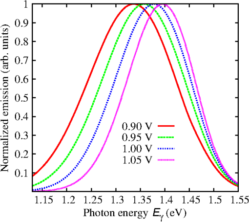
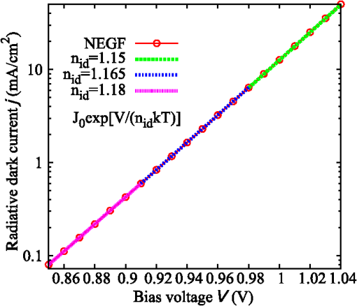
3.1.Field-Dependent Generation and Recombination in Ultra-Thin Film Absorber Solar CellsRecently, plasmonic concepts were presented for strong confinement of the incident light in absorber layers with thickness of only a few nm. 11 , 12 If such ultra-thin film solar cells remain based on bipolar junctions, such as the 40 nm GaAs diode with doping density of investigated here using the EMA with parameters given in Table 1, the doping-induced built-in potential is dropped over a very short distance (Fig. 1), which results in strong doping- and bias-dependent band tailing (Franz–Keldysh) effects on the absorptance (Fig. 2), and consequently on the shape of the monochromatic current–voltage characteristics (Fig. 3). The bias-dependent band tail leads not only to subgap absorption, but also to a red shifting of the emission spectra under electrical injection at forward bias (Fig. 4). The decrease of the field with increasing bias causes the ideality factor of the radiative dark current to shrink toward unity as the field-induced tunnel enhancement of the recombination process is reduced (Fig. 5). Fig. 1Band profile and local density of states of a 40-nm GaAs pin junction solar cell. The doped layers extend over 10 nm and provide a charge carrier density of . 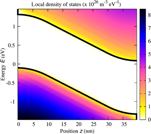 Fig. 2The strong built-in potential present in the ultra-thin junction leads to a Franz–Keldysh tailing of the band edge, inducing the absorption of sub-bandgap energy photons. Following the strength of the built-in field, the tailing (a) increases with doping density and (b) decreases with forward bias. The effect on the absorptance depends on the photon energy, whereas the absorption is increased at sub-bandgap energies, it is reduced above the band edge. 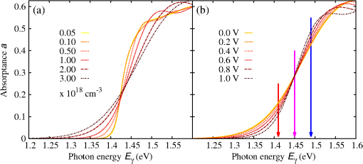 Fig. 3The bias dependence of the absorptance at different photon energies as displayed in Fig. 2 is reflected in the monochromatic current–voltage characteristics (@ ).  3.2.Photocarrier Transport in Quantum Well Superlattice Solar CellsQuantum well superlattice solar cells were proposed some time ago as tunable bandgap absorber components in multijunction solar cells. 13 Recently, absorber structures with strongly coupled quantum wells have shown enhanced carrier extraction efficiency as compared with multiquantum well structures with decoupled wells. 14 Conventional approaches to the simulation of quantum well superlattice solar cells assume either an infinite superlattice at flat band conditions and band-like semiclassical transport 15 or ballistic transport via the transfer matrix formalism. 16 Here, we use again the two-band EMA-NEGF approach. Figure 6 shows the local density of states of a 20 period, selectively contacted quantum well superlattice with barrier and well thicknesses of 1.5 and 2.5 nm, respectively, for (a) the flat band situation, corresponding to an intrinsic system and (b) a pin structure with strong built-in field induced by a doping density of . The strong coupling of the quantum wells results in a bulk-like density of states, however, exhibiting an confinement-induced increase in the effective bandgap as compared with bulk InGaAs. Both features are preserved in the presence of the large built-in field. Fig. 6Local density of states of a 20-period quantum well superlattice at vanishing bias voltage and (a) flat band conditions, corresponding to an intrinsic system, and (b) for a doping density of . Although the effective bandgap is increased as compared with bulk InGaAs because of confinement, the strong coupling results in a pronounced carrier delocalization and associated quasi-3D DOS. 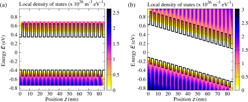 The (radiative) current–voltage characteristics of the 20-period superlattice structure are displayed in Fig. 7 for applied forward bias voltage in the dark and under monochromatic illumination with photons of an energy of 0.95 eV and at an intensity of . The current–voltage characteristics under illumination are perfectly reproduced by the superposition of the bias-dependent photocurrent as computed from the absorptance and the radiative dark current . Therefore, the charge carrier collection probability is close to unity even at large bias voltages in the vicinity of the maximum power point. Fig. 7Current voltage characteristics of the 20-period superlattice in the dark and under monochromatic illumination with photons of 0.95 eV and at . Because of the high degree of delocalization, the carrier escape probability is unity, i.e., the light JV-curve is the exact superposition of the bias-dependent photocurrent from the absorptance and the radiative dark current. 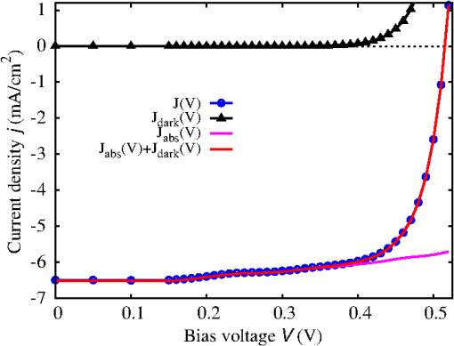 The charge carrier extraction can be investigated in more detail by considering the (spectral) current flow at different bias voltages. Figure 8 shows the current–voltage characteristics together with spectral and integral current flow, for (a) short-circuit conditions (0 V), (b) close to the maximum power point (0.45 V), (c) at open-circuit conditions (0.52 V), and (d) at open-circuit voltage in the dark. The sum of integral electron and hole currents is conserved at all bias voltages. As can be inferred from the current spectra, the minibands break up under realistic built-in fields, but at strong coupling, i.e., for thin barriers, carrier extraction proceeds almost ballistically. However, as shown in Fig. 9 for the structures of coupled 2.5-nm wide InGaAs with InAlGaAs barriers of thickness increasing from 1.5 to 3.5 nm, for thick barriers, the character of carrier transport changes from ballistic to sequential tunneling assisted by phonon-mediated relaxation. Thus, a rigorous assessment of carrier extraction in a given superlattice structure under realistic operating conditions is only provided at the quantum kinetic level. Fig. 8JV characteristics, integral and spectral current flow at (a) short-circuit conditions (0 V), (b) close to the maximum power point (0.45 V), (c) at open-circuit conditions (0.52 V), and (d) at open-circuit voltage in the dark. Although the minibands break up under realistic built-in fields, carrier extraction proceeds almost ballistically for thin barriers. 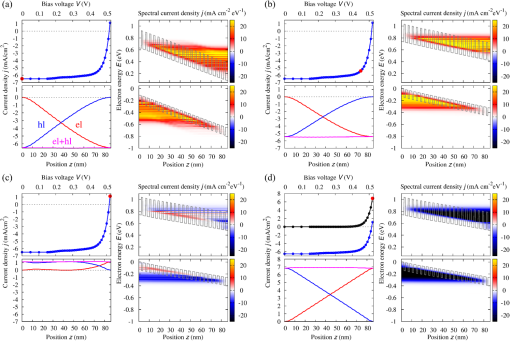 Fig. 9Photocurrent spectrum ( @0.95 eV) of coupled quantum well absorber structures with fixed InGaAs QW size of 2.5 nm and InAlGaAs layer thicknesses ranging from 1.5 to 3.5 nm. With increasing barrier width, the character of carrier transport gradually changes from quasi-ballistic to phonon-assisted sequential tunneling. 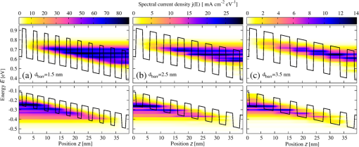 3.3.Absorption Losses in Double Quantum Well Tunnel Junctions for Multijunction Solar CellsIn high-efficiency multijunction solar cells, double quantum well structures have been proposed as tunnel junctions with high peak currents as well as low optical transmission losses. 17 In the junction region, the pronounced spatial variation of the doping profile gives rise to extreme band bending effects. As shown by recent NEGF simulations employing a tight-binding basis, 5 the strong fields result in large deviations of the local density of states from the situation at flat band conditions, apparent in both bulk injection and quantum well tunnel zones [Fig. 10(a)]. The local structure of bound and quasibound states in the junction region not only affects the tunneling transport of charge carriers, but also affects the local absorption coefficient [Fig. 10(b)]. The associated absorptance no longer reflects the joint density of states of either the bulk injection regions or a regular square well potential [Fig. 10(c)]. 4.ConclusionsThe strong local potential variations that are present in ultra-thin or nanostructure-based solar cell devices have a large impact on the photogeneration, photocarrier extraction, and radiative recombination processes, which is fully captured by the proposed NEGF-based simulation framework. Notable examples are strong field-induced band tailing effects in ultra-thin junction solar cells, with associated red shift in the absorption and emission spectra. It is further shown that the deviations from the flat band bulk picture are of special relevance for the assessment of carrier transport in superlattice solar cells and of the absorption losses in novel tunnel junction architectures for multijunction devices. References
U. Aeberhard
R. H. Morf
,
“Microscopic nonequilibrium theory of quantum well solar cells,”
Phys. Rev. B, 77
(12), 125343
(2008). http://dx.doi.org/10.1103/PhysRevB.77.125343 1098-0121 Google Scholar
U. Aeberhard
,
“Theory and simulation of photogeneration and transport in Si-SiO
x
superlattice absorbers,”
Nanoscale Res. Lett., 6 242
(2011). http://dx.doi.org/10.1186/1556-276X-6-242 1556-276X Google Scholar
U. Aeberhard
,
“Effective microscopic theory of quantum dot superlattice solar cells,”
Opt. Quantum Electron., 44
(3–5), 133
–140
(2012). http://dx.doi.org/10.1007/s11082-011-9529-9 0306-8919 Google Scholar
U. Aeberhard
et al.
,
“Fluorescence of colloidal PbSe/PbS QDs in NIR luminescent solar concentrators,”
Phys. Chem. Chem. Phys., 14
(47), 16223
–16228
(2012). http://dx.doi.org/10.1039/c2cp42213a 1463-9076 Google Scholar
U. Aeberhard
,
“Theoretical investigation of direct and phonon-assisted tunneling currents in InAlGaAs/InGaAs bulk and quantum-well interband tunnel junctions for multijunction solar cells,”
Phys. Rev. B, 87
(8), 081302
(2013). http://dx.doi.org/10.1103/PhysRevB.87.081302 1098-0121 Google Scholar
U. Aeberhard
,
“Simulation of absorption, photogeneration, and carrier extraction in nanostructure-based and ultra-thin film solar cell devices beyond the classical picture,”
Proc. SPIE, 8981 898103
(2014). http://dx.doi.org/10.1117/12.2040610 0277-786X Google Scholar
U. Aeberhard
,
“Theory and simulation of quantum photovoltaic devices based on the non-equilibrium Green’s function formalism,”
J. Comput. Electron., 10
(4), 394
–413
(2011). http://dx.doi.org/10.1007/s10825-011-0375-6 1569-8025 Google Scholar
U. Aeberhard
,
“Quantum-kinetic theory of photocurrent generation via direct and phonon-mediated optical transitions,”
Phys. Rev. B, 84
(3), 035454
(2011). http://dx.doi.org/10.1103/PhysRevB.84.035454 1098-0121 Google Scholar
U. Aeberhard
,
“Photon Green’s functions for a consistent theory of absorption and emission in nanostructure-based solar cell devices,”
Opt. Quantum Electron., 46
(6), 791
–796
(2014). http://dx.doi.org/10.1007/s11082-013-9790-1 0306-8919 Google Scholar
G. Mahan
,
“Quantum transport equation for electric and magnetic fields,”
Phys. Rep., 145
(5), 251
–318
(1987). http://dx.doi.org/10.1016/0370-1573(87)90004-4 0370-1573 Google Scholar
I. Massiot
et al.
,
“Nanopatterned front contact for broadband absorption in ultra-thin amorphous silicon solar cells,”
Appl. Phys. Lett., 101
(16), 163901
(2012). http://dx.doi.org/10.1063/1.4758468 0003-6951 Google Scholar
Z. Wang
T. P. White
K. Catchpole
,
“Plasmonic near-field enhancement for planar ultra-thin photovoltaics,”
IEEE Photon. J., 5
(5), 8400608
(2013). http://dx.doi.org/10.1109/JPHOT.2013.2280518 Google Scholar
M. A. Green
,
“Potential for low dimensional structures in photovoltaics,”
Mat. Sci. Eng. B, 74
(1–3), 118
–124
(2000). http://dx.doi.org/10.1016/S0921-5107(99)00546-2 0921-5107 Google Scholar
H. Fujii
et al.
,
“100-period, 1.23-eV bandgap InGaAs/GaAsP quantum wells for high-efficiency GaAs solar cells: toward current-matched Ge-based tandem cells,”
Prog. Photovolt: Res. Appl., 22
(7), 784
–795
(2014). http://dx.doi.org/10.1002/pip.v22.7 1062-7995 Google Scholar
T. Kirchartz
et al.
,
“Efficiency limits of Si/SiO2 quantum well solar cells from first-principles calculations,”
J. Appl. Phys., 105
(10), 104511
(2009). http://dx.doi.org/10.1063/1.3132093 0021-8979 Google Scholar
M. Courel
J. C. Rimada
L. Hernández
,
“GaAs/GaInNAs quantum well and superlattice solar cell,”
Appl. Phys. Lett., 100
(7), 073508
(2012). http://dx.doi.org/10.1063/1.3687195 0003-6951 Google Scholar
M. P. Lumb
et al.
,
“Double quantum-well tunnel junctions with high peak tunnel currents and low absorption for InP multijunction solar cells,”
Appl. Phys. Lett., 100
(21), 213907
(2012). http://dx.doi.org/10.1063/1.4722890 0003-6951 Google Scholar
BiographyUrs Aeberhard is a senior researcher at the Institute of Energy and Climate Research 5: Photovoltaics, Research Centre Jülich, Germany. He received a diploma degree in theoretical physics and PhD degree in condensed matter theory from the Swiss Federal Institute of Technology in Zurich (ETHZ) in 2004 and 2008, respectively. His current research interests include the theory and simulation of nanostructure-based solar cell devices. |

