|
|
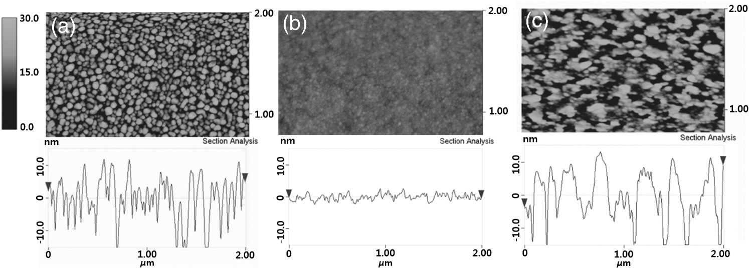
1.IntroductionTransparent conducting oxides (TCOs) can be used as transparent electrodes for various optoelectronic devices, such as organic light-emitting diodes (OLEDs) and organic solar cells (OSCs).1–9 Indium tin oxide (ITO) is widely used as a TCO due to its high optical transmittance (OT ) and good conductivity (sheet resistance ).10–12 However, ITO film has limitations due to its high growth temperature, high cost, and poor mechanical flexibility.13,14 Furthermore, ITO films are obtained using sputtering techniques, which can damage the underlying layers.15,16 Thus, significant research has been directed toward finding a suitable replacement for ITO. Nanostructured conducting materials such as Ag nanowires,17,18 graphenes,19 poly(3, 4-ethylenedioxythiophene) poly(styrenesulfonate) (PEDOT:PSS),20 metal grids,21–25 ITO nanobranch,26,27 and ZnO-doped 28 have been evaluated as flexible electrodes to overcome the shortcomings of ITO. Metal nanowires show high transmittance () and relatively low sheet resistance (), but poor thermal stability and rough surface morphology causing poor efficiency.29,30 Graphene, PEDOT:PSS, and ITO nanobranch have superior flexibility, but are limited by low conductivity and lack of uniformity in large areas.20,26,31 Metal grids have also been used for transparent electrodes, with excellent conductivity and flexibility. However, fabrication procedures are high cost and complex.21 One way to produce a transparent electrode is to incorporate a thin metal electrode. Metal/dielectric and dielectric/metal/dielectric structures combine the characteristics of high electrical conductivity of metals and good mechanical ductility of thin films.32–37 However, these structures have relatively low OT . Ultrathin Ag electrodes are promising for this function because the OT and of these electrodes are comparable to or better than those of ITO electrodes.38–49 In addition, their mechanical properties are appropriate for use in flexible devices.40 This review highlights recent progress in the fabrication of nanoscale thin Ag electrodes. It includes an introduction on the relevant theory and detailed discussion of the characteristics of ultrathin Ag film. To clarify the trends in ultrathin Ag electrode development, we organize them according to the methods used to form ultrathin Ag films. 2.Ag Electrodes for Organic ElectronicsSeveral studies have considered applications of Ag film to the electrode of organic electronics. Ag has the highest OT and lowest among metals, and is ductile.50,51,52 However, even though Ag has a high OT compared to other metals, a thin film of Ag () has a low OT compared to ITO film.53 Therefore, most Ag electrodes are used as semitransparent electrodes. Use of a semitransparent electrode can cause a microcavity effect, which improves the optical property of devices.50,54 Destructive interferences within the microcavity reduce the internal reflection of OLEDs. Ultrathin Ag electrodes are promising for this function because of OTs and s that are comparable to or better than those of ITO electrodes.50 The optical enhancement ratio varies according to metal film and dielectric material [Fig. 1(a)]. To maximize the microcavity effect, the thickness of each layer should be designed optically.54 Thin Ag electrodes can achieve an OSC performance that exceeds those of OSCs with ITO electrodes.50 The thickness of the active layer can be adjusted to maximize the electric field within the active layer [Fig. 1(b)]. The resulting microcavity resonant condition amplifies the electric field within the cell to give a higher performance than the ITO-based devices. Although microcavity effects can increase the device efficiency, its OT is degraded due to reflection and absorption by the Ag electrodes. Therefore, a microcavity is not appropriate for transparent displays, lighting, or solar cells. The irradiance that has been absorbed is given by the difference between the irradiance incident on the thickness element and the irradiance that emerges from the exit side.55 The irradiance absorbed by a layer is given by55 where is the average amplitude of the electric field in the film considered, is the free-space admittance, is the wavelength of irradiance, is the refractive index, is the extinction coefficient, and is the optical thickness. This equation demonstrates that can be decreased (OT can be increased) by reducing . ITO has a low . But among metals, only Ag and Au have a suitably low .27Fig. 1(a) Calculated enhancement ratio of the electrode relative to indium tin oxide as a function of the thickness of both Au and .54 Reprinted with permission from Ref. 54. Copyright 2012, Nature Publishing Group. (b) Electric field calculated by transfer matrix method considering a unitary incoming intensity for a 600 nm light wave (incident from the left).50 Reprinted with permission from Ref. 50. Copyright 2013, Wiley-VCH. 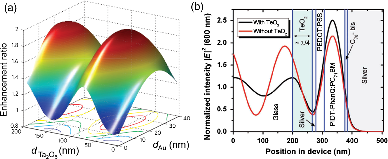 To maximize the OT of the Ag film, it must be as thin as possible. Generally, an OLED with an Ag electrode thick shows a narrow emission spectrum due to the strong cavity effect, and a weak intensity contribution in the undesigned wavelength region. Furthermore, emission color changes with the viewing angle. Therefore, Ag electrodes thick are not good for broad wavelength range applications such as white OLEDs. Several approaches to use an ultrathin () Ag electrode have been reported.38–49 As the OT of the electrode increases, its emission spectrum broadens, in agreement with theoretical expectations for a weak microcavity.56 Using a weak microcavity also increases the angular color stability and the device efficiency.44 3.Fundamental Principle on Conduction and Transmittance of Thin Ag FilmAgglomeration (growth of “islands”) is a transport process that reduces the overall energy of a system.57 In most heteroepitaxial systems, films grown on a foreign substrate energetically favor island growth and thus are subject to dewetting instability.58 This means that the interaction between substrate and Ag atoms is an important factor to determine the growth mode. Depending on the interaction energies of substrate atoms and film atoms, any of three growth modes (Frank-van der Merwe mode, Volmer-Weber mode, Stranski-Krastanov mode) can occur (Fig. 2).59 Layers of material grow one on top of another: this is called layer-by-layer growth (Frank-van der Merwe mode). Interaction between substrate and atoms in a film is greater than the distance between adjacent atoms in the film (Fig. 2). Ag layers exhibit three-dimensional (3-D) island growth (Volmer-Weber mode) as a result of the poor wettability of Ag on the substrate. Ag films have very low adhesion energy at the metal/oxide interface:60 this means that the Ag atoms interact more strongly with each other than with the substrate. Therefore, Ag films tend to form islands on the substrates; this process yields a rough and discontinuous surface. Fig. 2Initial states of film growth. , substrate surface coverage in monolayers (MLs).59 Reprinted with permission from Ref. 59. Copyright 2015, The Optical Society. 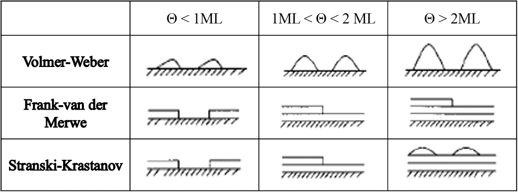 A discrete Ag film that consists of islands strongly absorbs and scatters light because of localized surface plasmon resonance (LSPR).39,61 LSPR results from the coupling between incident light and the free electron gas at the surface of a metal island structure.62 Coupling between light and free electron causes some light to be absorbed and some to be scattered. This coupling occurs at specific frequencies for each kind of metal. Ag has its LSPR frequency in the visible wavelength region. Glass/Ag samples show specific dips related to LSPR at wavelengths near 500 nm [Fig. 3(a)]. Simulations and experimental results did not match at a low Ag thickness because Ag film thick has many isolated clusters and voids. The of Ag on the bathocuproine increases as Ag thickness decreases [Fig. 3(b)] due to island growth of the Ag film, and is infinite at . The isolated metallic grains provide no sufficient conductive paths through the layer. However, after the percolation threshold is reached, separate metal islands start to connect and form a continuous layer: this process causes to decrease rapidly.63 To obtain a highly conductive and transparent Ag film, it must be continuous and smooth. Fig. 3(a) Total transmittance of the glass/Ag films as a function of Ag thickness (dotted line: simulation, solid line: experimental results). Commercial thin film simulator is used for simulation (The Essential Macleod, Thin Film Center Inc.) (b) Sheet resistance of Ag on BCP as a function of various Ag thicknesses.63 Reprinted with permission from Ref. 63. Copyright 2013, Wiley-VCH. 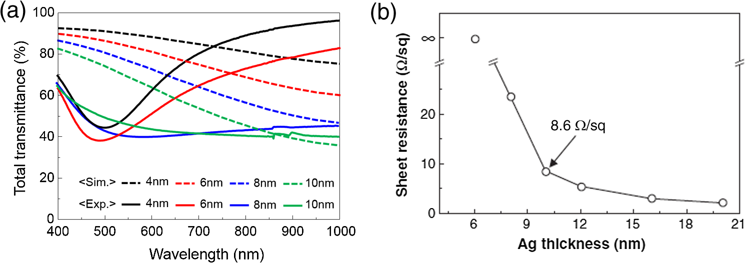 4.Recent Methods for Formation of Ultrathin Ag Film4.1.Seed LayerThe island growth of Ag occurs because the substrate has low surface energy compared to Ag ().64 The introduction of seed layers reduces the difference in between the substrate and Ag. Wetting of Ag layer on the substrate is significantly improved by adding seed materials such as Au, Al, Ca, Ge, Ni, , or .38–46 A Ca seed layer with , and an Al seed layer with reduce the difference in between the substrate and Ag.39 Schubert et al.39 obtained a continuous and smooth 7-nm thick Ag film using an Au seed layer. Because Au has a higher than does Ag, the attachment of Ag atoms to the Au surface is favored over agglomeration [Fig. 4(a)]. For a nominal thickness , glass/Ag samples have a low OT and high [Fig. 4(b)].38 The use of an Au seed layer causes the morphology of the Ag film to become very smooth and homogeneous, even for total thickness of the Ag layer . Compared to ITO, the Ag film with an Au seed layer has a similar OT and lower [Fig. 4(b)]. Fig. 4(a) Scanning electron micrographs of 7-nm thick silver layers deposited on p-doped N, N′-((diphenyl-N, N′-bis)9,9,-dimethyl-fluoren-2-yl)-benzidine which mimics the organic solar cell (OSC) and various seed layers with different surface energies taken from literature. The white scale bar represents 200 nm.39 Reprinted with permission from Ref. 39. Copyright 2013, Wiley-VCH. (b) Transmittance and sheet resistance of the different transparent electrodes are investigated here.38 Reprinted with permission from Ref. 38. Copyright 2013, Wiley-VCH. (c) Plot showing the average root mean square (RMS) surface roughness as a function of Ge thickness for a constant Ag thickness of 15 nm. The insets (a) and (b) show the contrast between a rough and a smooth surface for SEM images of without and with Ge (scale bar: ).65 Reprinted with permission from Ref. 65. Copyright 2009, American Chemical Society. 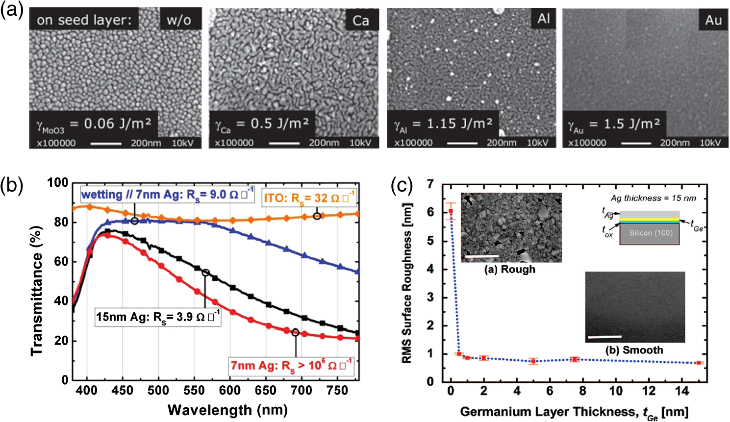 Seed layers such as Ge and promote nucleation of Ag.46,66 Williams et al. used a Ge seed layer to achieve a continuous Ag film.65 Although the Ge deposition on the substrate also caused island growth, the density of the Ge nuclei was much larger and the islands were significantly smaller than those for Ag deposited without a seed layer on the substrate. This surface provided a heterogeneous nucleation site for the deposited Ag atoms. The activation energy for Ag diffusion is on a Ge surface and on a surface.67 Therefore, using a Ge seed layer before depositing Ag reduces the surface diffusion and mass transportation of Ag, and results in a smooth and continuous Ag film. Compared to the topology between rough and smooth [Fig. 4(c), inset], without the layer of Ge, the deposited Ag formed distinct polycrystalline granular clusters with irregular shapes and a significant density of pinholes, which made the film electrically discontinuous. However, a Ge seed layer with thickness leads to a suppression of Ag island growth, thereby smoothing the film. The smoother Ag thin films also had a lower sheet resistance (, ).65 Metal and oxide can be used as good wetting layers in all device structures. 4.2.Surface TreatmentThe growth of Ag islands can also be reduced by derivatizing the substrate with a layer of molecules designed to enhance Ag nucleation by interacting strongly with both the substrate and the incoming Ag atoms.68 Zou et al.69 improved the Ag wetting property by applying a double-end functionalized 11-mercapto-undecanoic acid (MUA) self-assembled monolayer (SAM) on the substrate as a molecular binder to covalently attach Ag to the substrate. In the absence of a seed layer, discontinuous Ag islands grow on a glass substrate [Fig. 5(a)], but MUA can interact with the incident Ag atoms to form an ester linkage which minimizes surface diffusion and enhances Ag nucleation, so the Ag film is very smooth with a low root mean square roughness and reduced [Fig. 5(b)]. However, lauric acid SAM has an inert terminal group which leads to a significantly rough surface due to the growth of Ag islands [Fig. 5(c)]. To maximize the adhesion between the substrate and Ag, the appropriate SAM material must be chosen. 4.3.Low-Temperature DepositionTemperature can affect the growth of Ag islands. Even dewetting has been observed when the temperature exceeds 102°C.70,71 Ultrathin continuous Ag films are produced at low temperatures. A low substrate temperature generally reduces surface diffusion of Ag atoms, and thus alters the nucleation processes.72 Presland et al.73 defined induction time as the time at which the void density increases in the film during an isothermal anneal for a given film thickness; it is related to the activation energy of void formation as where is a pre-exponential factor, is the Boltzmann constant, and is the absolute annealing temperature. is comparable to that reported in the literature for the surface diffusion activation energy of an Ag thin film in a vacuum.74 Therefore, to reduce Ag agglomeration, should be increased and should be decreased. Sergeant et al.75 optimized several deposition parameters to minimize the growth of Ag islands by controlling the evaporation rate and substrate temperature. The best results were obtained at a deposition rate of 5.5 to onto a substrate cooled to . Increasing the evaporation rates and reducing the substrate temperature caused a reduction in the surface diffusion of Ag atoms: this means that sufficient nucleation sites are created to enhance the lateral growth of Ag films. Although a low-temperature process may be useful for the growth of ultrathin Ag layers, the process cost is high due to the requirement of the equipment needed to maintain a low temperature.4.4.Doping EffectIn a nonwetting system, flat ultrathin Ag films tend to transform to 3-D islands.76 This dewetting tendency of pure Ag becomes more obvious at elevated temperatures.57,77 Zhang et al.48 and Gu et al.49 used Al doping to fabricating ultrathin (3 nm) Ag-based thin films with high thermal stability on (100) substrates. Al doping yielded smaller and denser nuclei [Fig. 6(a)] than those in pure Ag films [Fig. 6(b)]: this difference reveals that Al doping causes an increase in the nuclei density of the films. Al-O bonds are much stronger than Ag-O bonds60 so Al atoms are immobilized on the substrate and can hinder the diffusion of Ag atoms; therefore, Al-doping causes increased spatial density of nuclei and reduced size of particles. Figures 6(c) and 6(e) show the SEM images of 15 nm as-deposited pure Ag and Al-doped Ag films. Due to dewetting, pure Ag film easily changes to isolated islands after annealing at 300°C [Fig. 6(d)]. In contrast, an Al-doped Ag film shows an ultrasmooth surface morphology that is very similar to that of the as-deposited surface [Fig. 6(f)]. These results show that Al doping is a very effective method to form an ultrathin Ag layer with high thermal stability. Wang et al.47 used oxygen doping to achieve an ultrathin Ag-based film. The oxygen-doped Ag () layer was 6-nm thick and was completely continuous and smooth. Oxygen doping of the ultrathin Ag layer improved its OT without any noticeable degradation of electrical conductivity. Fig. 6Two-dimensional AFM images of (a) 3 nm pure Ag films, (b) 3 nm Al-doped Ag films on (100) substrates. SEMs () of (c) 15 nm as-deposited and (d) annealed pure Ag films on in at 300°C (e) 15 nm as-deposited and (f) annealed Al-doped Ag films on in at 300°C. The insets in (e) and (f) are AFM images of 15 nm as-deposited and annealed Al-doped Ag films on with an RMS roughness of 0.43 and 0.45 nm, respectively.49 Reprinted with permission from Ref. 49. Copyright 2014, American Chemical Society.  5.Application and Developments5.1.Organic Light-Emitting Diode Lighting and Organic Solar Cell with a High PerformanceMonochromatic top-emitting OLEDs based on thin metal electrodes show high efficiency due to their microcavity structure. However, as a result of spectral narrowing and change of emission color with viewing angle, white OLEDs show low efficiency and color quality.78,79 To achieve highly efficient white OLEDs, the OT of the transparent electrode must be increased. Schwab et al.38 used an ultrathin Ag electrode to improve the characteristics of the top electrode, and achieved better color quality and color stability compared to those of an optimized white OLED based on an ITO electrode. The highly transparent ultrathin Ag electrode increased the spectral width of the microcavity [Fig. 7(a), red line] and increased the luminous efficacy by 25% compared to a standard Ag electrode. Fig. 7(a) Normalized spectral radiant intensity measured at current density of for the different OLEDs investigated in this study. A hole transport layer (HTL) thickness in the wetting layer device is optimized to 50 nm.38 Reprinted with permission from Ref. 38. Copyright 2013, Wiley-VCH. (b) EQE spectra of OSCs using different transparent electrodes. Inset: specular transmittances.47 Reprinted with permission from Ref. 47. Copyright 2013, Wiley-VCH. 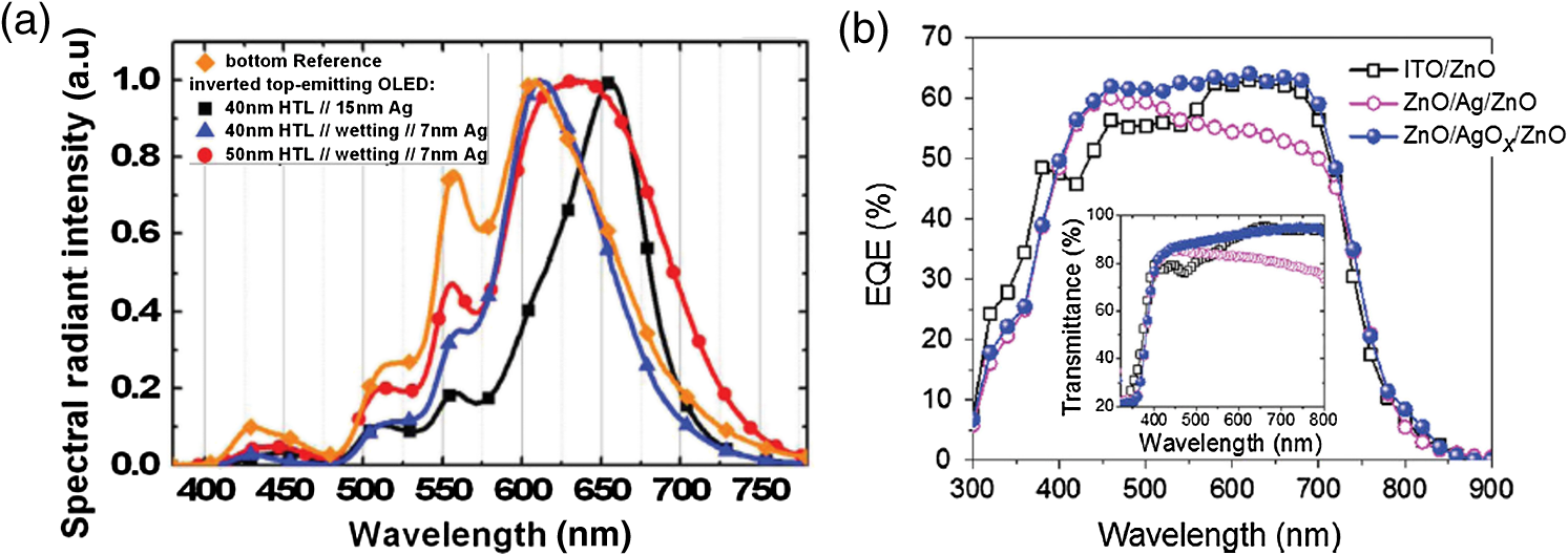 Wang et al.47 demonstrated a highly transparent ultrathin Ag electrode for flexible inverted OSCs, and it achieved a higher power conversion efficiency (PCE) and external quantum efficiency (EQE) than did conventional ITO-based OCSs [Fig. 7(b)]. The PCE and EQE enhancements using an ultrathin oxygen doped electrode were mainly the result of its increased OT [Fig. 7(b), inset]. The electrode provided an at 620 nm: this is the highest value achieved by any flexible OSC fabricated on polymer substrates. OSCs fabricated on a thin metal electrode show enhanced PCEs due to the optical cavity effect. The method of tuning the optical cavity in a device is to change the thickness of the layers between reflective and semitransparent metal electrodes, with the objective of changing the length of the optical path.54 Some groups have tuned the optical cavity to improve the performance of OSCs. To maximize the photocurrent, the thickness of the hole transport layer (HTL) can be optimized to the optical cavity so that the resonance frequency occurs in a spectral range in which light absorption by the absorber is weak.75 This tuning increased the optical characteristics such as high fill factor, open circuit voltage, and PCE by up to 4.4%, so the HTLs are attractive replacements for ITO electrodes in OSCs.75 A 7 nm Al-doped Ag-based device with a resonance cavity in the active layer between the reflective anode and the semitransparent ultrathin Al-doped Ag cathode has a spectrum peak that is close to the absorption edge of a photoactive absorber.48 5.2.Flexible Device ApplicationITO-based flexible optoelectronic devices show a dramatically decreased performance during bending. A flexible OSC that uses an Ag electrode with a seed layer showed stable performance even after bending cycles ().50 Wang et al. demonstrated a flexible OSC that uses an ultrathin electrode [Fig. 8(a)].47 The percentage change in of the ITO electrode was 35% higher than that of the electrode at the same bending radius as a result of the formation and propagation of microscopic cracks in the ITO [Fig. 8(b), inset]. However, the of the ultrathin Ag electrode changed little under bending stress, and formed no cracks on the film surface. Figure 8(c) shows the device architecture of the flexible OSC using an ultrathin Ag electrode. As the bending radius decreased, the PCE of the ITO-based OSC greatly decreased, but that of the ultrathin Ag-based OSC was not severely affected [Fig. 8(d)]. Compared to ITO-based OSCs, the higher flexibility of the ultrathin Ag electrode ensured the superior structural durability of OSCs. Fig. 8(a) Photographs of irreversible bending tests of flexible transparent conducting electrodes (TCEs) coated on the polyethylene terephthalate (PET) substrates. (b) The percentage change in the resistance of the TCEs as a function of the bending radius. Insets represent the optical images of the TCEs after being bent with a bending radius of 2.8 mm. (c) Device architecture of flexible OSC fabricated on a PET substrate used in this study. (d) Power conversion efficiency values measured for flexible OSCs as a function of bending radius during compressive bending, normalized to the initial value. Inset: fabricated flexible OSC using ultrathin Ag electrode on a PET substrate.47 Reprinted with permission from Ref. 47. Copyright 2013, Wiley-VCH. 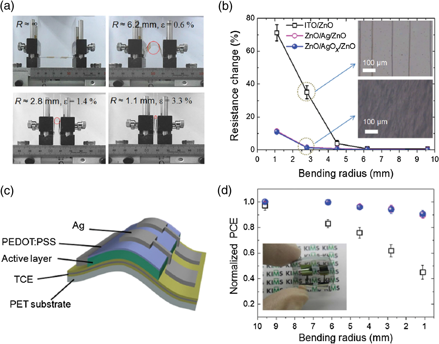 6.SummaryUltrathin Ag electrodes are promising candidates as next-generation flexible transparent electrodes. Compared with other transparent electrodes, these ultrathin metal-based transparent electrodes have the highest OT, flexibility, and low . However, growth of 3-D Ag islands causes strong absorption and scattering of incident light: because of LSPR, and these phenomena degrade its transparency. Smooth and ultrathin Ag layers () could be produced by introducing a seed layer, by using surface treatment, by low-temperature deposition, and by doping. The high OT of the ultrathin Ag electrode can improve the color quality and color stability of white OLEDs that use a weak microcavity structure.38,40,44 Ultrathin Ag electrodes have been used to achieve the highest EQE of any flexible OSC fabricated on polymer substrates.47 Ultrathin Ag-based electrodes provide opportunities to demonstrate highly flexible and transparent optoelectronic applications. However, several disadvantages of ultrathin Ag electrodes remain to be overcome; these include light absorption by the seed layer, a trade-off between OT and when changing the thickness of Ag films and low thermal stability. AcknowledgmentsThis research was financially supported by the National Research Foundation (NRF) of Korea grant funded by the Korean government (MEST) (No. NRF-2013R1A2A2A01069237). ReferencesP. Gorrn et al.,
“Towards see-through displays: fully transparent thin-film transistors driving transparent organic light-emitting diodes,”
Adv. Mater., 18
(6), 738
–741
(2006). http://dx.doi.org/10.1002/adma.200501957 ADVMEW 0935-9648 Google Scholar
G. Gu et al.,
“Transparent flexible organic light-emitting devices,”
Adv. Mater., 9
(9), 725
–728
(1997). http://dx.doi.org/10.1002/adma.19970090910 ADVMEW 0935-9648 Google Scholar
S. Reineke et al.,
“White organic light-emitting diodes with fluorescent tube efficiency,”
Nature, 459 234
–238
(2009). http://dx.doi.org/10.1038/nature08003 NATUAS 0028-0836 Google Scholar
W. J. Dong et al.,
“Effect of ultra-violet-ozone on ITO/P3HT interface for PEDOT:PSS-free polymer solar cells,”
Sol. Energy Mater. Sol. Cells, 109 240
–245
(2013). http://dx.doi.org/10.1016/j.solmat.2012.10.023 SEMCEQ 0927-0248 Google Scholar
K. Hong et al.,
“Enhanced light out-coupling of organic light emitting diodes: spontaneously formed nano-facet structured MgO as a refractive index modulation layer,”
Adv. Mater., 22
(43), 4890
–4894
(2010). http://dx.doi.org/10.1002/adma.201002028 ADVMEW 0935-9648 Google Scholar
W. J. Dong, G. H. Jung and J.-L. Lee,
“Solution-processed- hole extraction layer on oxygen plasma treated indium tin oxide in organic photovoltaics,”
Sol. Energy Mater. Sol. Cells, 116 94
–101
(2013). http://dx.doi.org/10.1016/j.solmat.2013.04.005 SEMCEQ 0927-0248 Google Scholar
K. Hong and J.-L. Lee,
“Review paper: recent developments in light extraction technologies of organic light emitting diodes,”
Electron. Mater. Lett., 2
(1), 021215
(2012). http://dx.doi.org/10.1007/s13391-011-0601-1 EMLLAE 1738-8090 Google Scholar
S. Loser et al.,
“High-efficiency inverted polymer photovoltaics via spectrally tuned absorption enhancement,”
Adv. Energy Mater., 4
(14), 1301938
(2014). http://dx.doi.org/10.1002/aenm.201301938 ADEMBC 1614-6840 Google Scholar
N. Li et al.,
“Environmentally printing efficient organic tandem solar cells with high fill factors: a guideline towards 20% power conversion efficiency,”
Adv. Energy Mater., 4
(11), 140084
(2014). http://dx.doi.org/10.1002/aenm.201400084 ADEMBC 1614-6840 Google Scholar
S. Reineke et al.,
“White organic light-emitting diodes with fluorescent tube efficiency,”
Nature, 459 234
–238
(2009). http://dx.doi.org/10.1038/nature08003 NATUAS 0028-0836 Google Scholar
R. Capelli et al.,
“Organic light-emitting transistors with an efficiency that outperforms the equivalent light-emitting diodes,”
Nat. Mater., 9 496
–503
(2010). http://dx.doi.org/10.1038/nmat2751 NMAACR 1476-1122 Google Scholar
D. Joly et al.,
“White organic light-emitting diodes based on quench-resistant fluorescent organophosphorus dopants,”
Adv. Funct. Mater., 22
(3), 567
–576
(2012). https://doi.org/ttp://dx.doi.org/10.1002/adfm.201102005 AFMDC6 1616-3028 Google Scholar
C. Feng et al.,
“Flexible, stretchable, transparent conducting films made from superaligned carbon nanotubes,”
Adv. Funct. Mater., 20
(6), 885
–891
(2010). http://dx.doi.org/10.1002/adfm.200901960 AFMDC6 1616-3028 Google Scholar
J. Meyer et al.,
“Transparent inverted organic light-emitting diodes with a tungsten oxide buffer layer,”
Adv. Mater., 20
(20), 3839
–3843
(2008). http://dx.doi.org/10.1002/adma.200800949 ADVMEW 0935-9648 Google Scholar
S. Y. Ryu et al.,
“Highly efficient transparent organic light-emitting diodes by ion beam assisted deposition-prepared indium tin oxide cathode,”
Appl. Phys. Lett., 90
(3), 033513
(2007). http://dx.doi.org/10.1063/1.2433032 APPLAB 0003-6951 Google Scholar
C.-H. Chung et al.,
“Improvement in performance of transparent organic light-emitting diodes with increasing sputtering power in the deposition of indium tin oxide cathode,”
Appl. Phys. Lett., 86
(9), 093504
(2005). http://dx.doi.org/10.1063/1.1869534 APPLAB 0003-6951 Google Scholar
K. Ziberberg et al.,
“Highly robust indium-free transparent conductive electrodes based on composites of silver nanowires and conductive metal oxides,”
Adv. Funct. Mater., 24
(12), 1671
–1678
(2014). http://dx.doi.org/10.1002/adfm.201303108 AFMDC6 1616-3028 Google Scholar
J.-W. Lim et al.,
“Simple brush-painting of flexible and transparent Ag nanowire network electrodes as an alternative ITO anode for cost-efficient flexible organic solar cells,”
Sol. Energy Mater. Sol. Cells, 107 348
–354
(2012). http://dx.doi.org/10.1016/j.solmat.2012.07.012 SEMCEQ 0927-0248 Google Scholar
S. Pang et al.,
“Graphene as transparent electrode material for organic electronics,”
Adv. Mater., 23
(25), 2779
–2795
(2011). http://dx.doi.org/10.1002/adma.201100304 ADVMEW 0935-9648 Google Scholar
Y. H. Kim et al.,
“Achieving high efficiency and improved stability in ITO-free transparent organic light-emitting diodes with conductive polymer electrodes,”
Adv. Funct. Mater., 23
(30), 3763
–3769
(2013). http://dx.doi.org/10.1002/adfm.201203449 AFMDC6 1616-3028 Google Scholar
M. G. Kang and L. J. Guo,
“Nanoimprinted semitransparent metal electrodes and their application in organic light-emitting diodes,”
Adv. Mater., 19
(10), 1391
–1396
(2007). http://dx.doi.org/10.1002/adma.200700134 ADVMEW 0935-9648 Google Scholar
C. Min et al.,
“Enhancement of optical absorption in thin-film organic solar cells through the excitation of plasmonic modes in metallic gratings,”
Appl. Phys. Lett., 96
(13), 133302
(2010). http://dx.doi.org/10.1063/1.3377791 APPLAB 0003-6951 Google Scholar
M.-G. Kang et al.,
“Efficiency enhancement of organic solar cells using transparent plasmonic Ag nanowire electrodes,”
Adv. Mater., 22
(39), 4378
–4383
(2010). http://dx.doi.org/10.1002/adma.201001395 ADVMEW 0935-9648 Google Scholar
P. B. Catrysse and S. Fan,
“Nanopatterned metallic films for use as transparent conductive electrodes in optoelectronic devices,”
Nano Lett., 10
(8), 2944
–2949
(2010). http://dx.doi.org/10.1021/nl1011239 NALEFD 1530-6984 Google Scholar
B. Zeng, Z. H. Kafafi and F. J. Bartoli,
“Transparent electrodes based on two-dimensional Ag nanogrids and double one-dimensional Ag nanogratings for organic photovoltaics,”
J. Photon. Energy, 5
(1), 057005
(2014). http://dx.doi.org/10.1117/1.JPE.5.057005 Google Scholar
H. K. Yu et al.,
“Three-dimensional nano-branched indium-tin-oxide for organic solar cells,”
ACS Nano, 5
(10), 8026
–8032
(2011). http://dx.doi.org/10.1021/nn2025836 1936-0851 Google Scholar
H. K. Yu et al.,
“Nano-branched transparent conducting oxide: beyond the brittleness limit for the flexible electrode applications,”
Nanoscale, 4
(21), 6831
–6834
(2012). http://dx.doi.org/10.1039/c2nr32228e 1556-276X Google Scholar
K. Kwak, K. Cho and S. Kim,
“Stable bending performance of flexible organic light-emitting diodes using IZO anodes,”
Sci. Rep., 3 2787
(2013). http://dx.doi.org/10.1038/srep02787 SRCEC3 2045-2322 Google Scholar
A. Kumar and C. Zhou,
“The race to replace tin-doped oxide: which material will win?,”
ACS Nano, 4
(1), 11
–14
(2010). http://dx.doi.org/10.1021/nn901903b 1936-0851 Google Scholar
J.-Y. Lee et al.,
“Solution-processed metal nanowire mesh transparent electrodes,”
Nano Lett., 8
(2), 689
–692
(2008). http://dx.doi.org/10.1021/nl073296g NALEFD 1530-6984 Google Scholar
J. O. Hwang et al.,
“Work function-tunable, n-doped reduced graphene transparent electrodes for high-performance polymer light-emitting diodes,”
ACS Nano, 6
(1), 159
–167
(2012). http://dx.doi.org/10.1021/nn203176u 1936-0851 Google Scholar
D. Poitras, C.-C. Kuo and C. Py,
“Design of high-contrast OLEDs with microcavity effect,”
Opt. Express, 16
(11), 8003
–8015
(2008). http://dx.doi.org/10.1364/OE.16.008003 OPEXFF 1094-4087 Google Scholar
M. Thomschke et al.,
“Optimized efficiency and angular emission characteristics of white top-emitting organic electroluminescent diodes,”
Appl. Phys. Lett., 94
(8), 083303
(2009). http://dx.doi.org/10.1063/1.3088854 APPLAB 0003-6951 Google Scholar
P. Freitag et al.,
“White top-emitting organic light-emitting diodes with forward directed emission and high color quality,”
Org. Electron., 11
(10), 1676
–1682
(2010). http://dx.doi.org/10.1016/j.orgel.2010.07.017 1566-1199 Google Scholar
K. Hong et al.,
“Optical properties of WO3/Ag/WO3 multilayer as transparent cathode in top-emitting organic light emitting diodes,”
J. Phys. Chem. C, 115
(8), 3453
–3459
(2011). http://dx.doi.org/10.1021/jp109943b 1932-7447 Google Scholar
J. Y. Ham et al.,
“Design of broadband transparent electrodes for flexible organic solar cells,”
J. Mater. Chem. A, 1
(9), 3076
–3082
(2013). http://dx.doi.org/10.1039/C2TA00946C Google Scholar
S. Kim et al.,
“MgO nano-facet embedded silver-based dielectric/metal/dielectric transparent electrode,”
Opt. Express, 20
(2), 845
–853
(2012). http://dx.doi.org/10.1364/OE.20.000845 OPEXFF 1094-4087 Google Scholar
T. Schwab et al.,
“Highly efficient color stable inverted white top-emitting OLEDs with ultra-thin wetting layer top electrodes,”
Adv. Opt. Mater., 1
(10), 707
–713
(2013). http://dx.doi.org/10.1002/adom.201300241 AOMDAX 2195-1071 Google Scholar
S. Schubert et al.,
“Improvement of transparent metal top electrodes for organic solar cell by introducing a high surface energy seed layer,”
Adv. Energy Mater., 3
(4), 438
–443
(2013). http://dx.doi.org/10.1002/aenm.201200903 ADEMBC 1614-6840 Google Scholar
S. Liu et al.,
“Silver/germanium/silver: an effective transparent electrode for flexible organic light-emitting devices,”
J. Mater. Chem. C, 2
(5), 835
–840
(2014). http://dx.doi.org/10.1039/C3TC31927J Google Scholar
P. Melpignano et al.,
“E-beam deposited ultra-smooth silver thin film on glass with different nucleation layers: an optimization study for OLED micro-cavity application,”
Org. Electron., 11
(6), 1111
–1119
(2010). http://dx.doi.org/10.1016/j.orgel.2010.03.022 1566-1199 Google Scholar
J. Meiss, M. K. Riede and K. Leo,
“Optimizing the morphology of metal multilayer films for indium tin oxide (ITO)-free inverted organic solar cells,”
J. Appl. Phys. Lett., 105
(6), 063108
(2009). http://dx.doi.org/10.1063/1.3100039 JAPLD8 0021-4922 Google Scholar
G. W. Hyung et al.,
“Bottom-emission organic light-emitting diodes using semitransparent anode electrode by O2 plasma,”
Org. Electron., 13
(11), 2594
–2599
(2012). http://dx.doi.org/10.1016/j.orgel.2012.07.020 1566-1199 Google Scholar
T. Schwab et al.,
“Eliminating micro-cavity effects in white top-emitting OLEDs by ultra-thin metallic top electrodes,”
Adv. Opt. Mater., 1
(12), 921
–925
(2013). http://dx.doi.org/10.1002/adom.201300392 AOMDAX 2195-1071 Google Scholar
S. Schubert et al.,
“Oxide sandwiched metal thin-film electrodes for long-term stable organic solar cells,”
Adv. Funct. Mater., 22
(23), 4993
–4999
(2012). http://dx.doi.org/10.1002/adfm.201201592 AFMDC6 1616-3028 Google Scholar
H. Cho, J.-M. Choi and S. Yoo,
“Highly transparent organic light-emitting diodes with a metallic top electrode: the dual role of a layer,”
Opt. Express, 19
(2), 1113
–1121
(2011). http://dx.doi.org/10.1364/OE.19.001113 OPEXFF 1094-4087 Google Scholar
W. Wang et al.,
“Transparent ultrathin oxygen-doped silver electrodes for flexible organic solar cells,”
Adv. Funct. Mater., 24
(11), 1551
–1561
(2014). http://dx.doi.org/10.1002/adfm.201301359 AFMDC6 1616-3028 Google Scholar
C. Zhang et al.,
“An ultrathin, smooth, and low-loss al-doped Ag film and its application as a transparent electrode in organic photovoltaics,”
Adv. Mater., 26
(32), 5696
–5701
(2014). http://dx.doi.org/10.1002/adma.201306091 ADVMEW 0935-9648 Google Scholar
D. Gu et al.,
“Ultrasmooth and thermally stable silver-based thin films with subnanometer roughness by aluminum doping,”
ACS. Nano, 8
(10), 10343
–10351
(2014). http://dx.doi.org/10.1021/nn503577c 1936-0851 Google Scholar
J. Salinas et al.,
“Optical design of transparent thin metal electrodes to enhance in-coupling and trapping of light in flexible polymer solar cells,”
Adv. Mater., 24
(47), 6362
–6367
(2012). http://dx.doi.org/10.1002/adma.201203099 ADVMEW 0935-9648 Google Scholar
S. Kim et al.,
“Design of red, green, blue transparent electrodes for flexible optical devices,”
Opt. Express, 22
(S5), 1257
–1269
(2014). http://dx.doi.org/10.1364/OE.22.0A1257 OPEXFF 1094-4087 Google Scholar
S. Kim and J.-L. Lee,
“Design of dielectric/metal/dielectric transparent electrode for flexible electronics,”
J. Photon. Energy, 2
(1), 021215
(2012). http://dx.doi.org/10.1117/1.JPE.2.021215 Google Scholar
K. Hong and J.-L. Lee,
“Inverted top-emitting organic light-emitting diodes using transparent silver oxide anode formed by oxygen plasma,”
Electrochem. Solid State Lett., 11
(2), H29
–H31
(2008). http://dx.doi.org/10.1149/1.2817479 ESLEF6 1099-0062 Google Scholar
Z. B. Wang et al.,
“Unlocking the full potential of organic light-emitting diodes on flexible plastic,”
Nat. Photon., 5 753
–757
(2011). http://dx.doi.org/10.1038/nphoton.2011.259 1749-4885 Google Scholar
H. A. Macleod, Thin-Film Optical Filters, 64 Thin Film Center, Arizona
(1986). Google Scholar
V. Bulovic et al.,
“Weak microcavity effects in organic light-emitting devices,”
Phys. Rev. B, 58 3730
–3740
(1998). http://dx.doi.org/10.1103/PhysRevB.58.3730 PRBMDO 1098-0121 Google Scholar
H. C. Kim, T. L. Alford and D. R. Allee,
“Thickness dependence on the thermal stability of silver thin films,”
Appl. Phys. Lett., 81
(22), 4287
–4289
(2002). http://dx.doi.org/10.1063/1.1525070 APPLAB 0003-6951 Google Scholar
K. Thurmer, E. D. Williams and J. E. Reutt-Rovey,
“Dewetting dynamics of ultrathin silver films on Si(111),”
Phys. Rev. B, 68 155423
(2003). http://dx.doi.org/10.1103/PhysRevB.68.155423 PRBMDO 1098-0121 Google Scholar
N. Kaiser,
“Review of the fundamentals of thin-film growth,”
Appl. Opt., 41
(16), 3053
–3060
(2002). http://dx.doi.org/10.1364/AO.41.003053 APOPAI 0003-6935 Google Scholar
C. T. Campbell,
“Ultrathin metal films and particles on oxide surface: structural, electronic and chemisorptive properties,”
Surf. Sci. Rep., 27
(1–3), 1
–111
(1997). http://dx.doi.org/10.1016/S0167-5729(96)00011-8 SSREDI 0167-5729 Google Scholar
K. Hong et al.,
“Design rules for highly transparent electrodes using dielectric constant matching of metal oxide with Ag film in optoelectronic devices,”
Chem. Commun., 48
(86), 10606
–10608
(2012). http://dx.doi.org/10.1039/c2cc35713e CHCOFS 1364-548X Google Scholar
E. A. Coronado, E. R. Encina and F. D. Stefani,
“Optical properties of metallic nanoparticles: manipulating light, heat and forces at the nanoscale,”
Nanoscale, 3
(10), 4042
–4059
(2011). http://dx.doi.org/10.1039/c1nr10788g 1556-276X Google Scholar
G. H. Jung et al.,
“ transparent cathodes for organic photovoltaics,”
Adv. Energy Mater., 1
(6), 1023
–1028
(2011). http://dx.doi.org/10.1002/aenm.201100411 ADEMBC 1614-6840 Google Scholar
L. Vitos et al.,
“The surface energy of metals,”
Surf. Sci., 411
(1–2), 186
–202
(1998). http://dx.doi.org/10.1016/S0039-6028(98)00363-X SUSCAS 0039-6028 Google Scholar
V. J. Logeeswaran et al.,
“Ultrasmooth silver thin films deposited with a germanium nucleation layer,”
Nano Lett., 9
(1), 178
–182
(2009). http://dx.doi.org/10.1021/nl8027476 NALEFD 1530-6984 Google Scholar
C. Cioarec et al.,
“Ultrasmooth silver thin film electrodes with high polar liquid wettability for OLED microcavity application,”
Langmuir, 27
(7), 3611
–3617
(2011). http://dx.doi.org/10.1021/la104760a LANGD5 0743-7463 Google Scholar
E. G. Seebauer and C. E. Allen,
“Estimating surface diffusion coefficients,”
Prog. Surf. Sci., 49
(3), 265
–330
(1995). http://dx.doi.org/10.1016/0079-6816(95)00039-2 PSSFBP 0079-6816 Google Scholar
H. M. Stec et al.,
“Ultrathin transparent Au electrodes for organic photovoltaics fabricated using a mixed mono-molecular nucleation layer,”
Adv. Funct. Mater., 21
(9), 1709
–1716
(2011). http://dx.doi.org/10.1002/adfm.201002021 AFMDC6 1616-3028 Google Scholar
J. Zou et al.,
“Interfacial engineering of ultrathin metal film transparent electrode for flexible organic photovoltaic cells,”
Adv. Mater., 26
(22), 3618
–3623
(2014). http://dx.doi.org/10.1002/adma.201306212 ADVMEW 0935-9648 Google Scholar
H. C. Kim, T. L. Alford and D. R. Allee,
“Thickness dependence on the thermal stability of silver thin films,”
Appl. Phys. Lett., 81
(4287),
(2002). http://dx.doi.org/10.1063/1.1525070 APPLAB 0003-6951 Google Scholar
J. H. Son et al.,
“Effect of reflective P-type ohmic contact on thermal reliability of vertical InGaN/GaN LEDs,”
Electron. Mater. Lett., 10
(6), 1171
–1174
(2014). http://dx.doi.org/10.1007/s13391-014-4127-1 EMLLAE 1738-8090 Google Scholar
R. S. Sennett and G. D. Scott,
“The structure of evaporated metal films and their optical properties,”
J. Opt. Soc. Am., 40
(4), 203
–211
(1950). http://dx.doi.org/10.1364/JOSA.40.000203 JOSAAH 0030-3941 Google Scholar
A. E. B. Presland, G. L. Price and D. L. Trimn,
“Kinetics of hillock and island formation during annealing of thin silver films,”
Prog. Surf. Sci., 3
(1), 63
–96
(1972). http://dx.doi.org/10.1016/0079-6816(72)90006-8 PSSFBP 0079-6816 Google Scholar
R. E. Hummel and H. J. Geier,
“Activation energy for electrotransport in thin silver and gold films,”
Thin Solid Films, 25
(2), 335
–342
(1975). http://dx.doi.org/10.1016/0040-6090(75)90053-X THSFAP 0040-6090 Google Scholar
N. P. Sergeant et al.,
“Design of transparent anodes for resonant cavity enhanced light harvesting in organic solar cells,”
Adv. Mater., 24
(6), 728
–732
(2012). http://dx.doi.org/10.1002/adma.201104273 ADVMEW 0935-9648 Google Scholar
H. Yu et al.,
“Quantitative determination of the metastability of flat Ag overlayers on GaAs (110),”
Phys. Rev. Lett., 88
(1), 016102
(2001). http://dx.doi.org/10.1103/PhysRevLett.88.016102 PRLTAO 0031-9007 Google Scholar
H. Krishna et al.,
“Thickness-dependent spontaneous dewetting morphology of ultrathin Ag films,”
Nanotechnology, 21
(15), 155601
(2010). http://dx.doi.org/10.1088/0957-4484/21/15/155601 NNOTER 0957-4484 Google Scholar
S. Hofmann et al.,
“Top-emitting organic light-emitting diodes,”
Opt. Express, 19
(S6), A1250
–A1264
(2011). http://dx.doi.org/10.1364/OE.19.0A1250 OPEXFF 1094-4087 Google Scholar
P. Freitag et al.,
“White top-emitting organic light-emitting diodes with forward directed emission and high color quality,”
Org. Electron., 11
(10), 1676
–1682
(2010). http://dx.doi.org/10.1016/j.orgel.2010.07.017 1566-1199 Google Scholar
BiographyIllhwan Lee received his BS degree in materials science and engineering from Hanyang University in 2009 and his MS degree in materials science and engineering from POSTECH in 2011. He is currently a PhD candidate in Professor Jong-Lam Lee's research group at POSTECH. His research interests include design of flexible transparent electrodes and architecture of nanostructured light out-coupling layers for optical devices. Jong-Lam Lee received a PhD degree in materials science and engineering from KAIST in 1985. He joined POSTECH in 1996. He is heading the Department of Materials Science and Engineering and was selected as a POSTECH fellow. His research covers architecture of nanostructures for photon extraction, flexible substrates for printing processes of flexible displays, and design of photonic devices. He published more than 300 papers in academic journals. |