|
|
1.IntroductionThe global cumulative installed photovoltaic capacity reached 180 GW by the end of the year 2014.1 More than 90% of the photovoltaic market is based on bulk-silicon solar cells,1 as manufacturing costs continue to fall.2 However, alternative solar-cell technologies are being pursued for niche applications. Thus, research on amorphous-silicon-based thin-film solar cells continues as these cells have two advantages: first, liquid crystal display technology can be used for deposition of silicon; second, large-area glass panels ( and higher) can be used for fabricating ultra-low-cost solar cells. While other materials such as CdTe, CIGS, and organic perovskites may seem promising for special purposes, silicon-based technologies are far better developed to date, both theoretically and technologically, for long-lasting and reliable performance.3–5 A variety of light-management strategies may be employed to boost light absorption and the production of electron–hole pairs (EHPs) inside the semiconductor region of a solar cell.5 These strategies include texturing the front surface6,7 and the metallic back reflector,8–10 coating the front surface with an antireflection layer,11,12 embedding metal nanoparticles inside the undoped layers of the semiconductor,13–15 and the use of light concentrators.16–18 Our attention is currently focused on the following three strategies for boosting the efficiency of thin-film solar cells:
Does the enhanced optical absorption due to the adoption of a set of light-management strategies transform into enhanced photovoltaic electricity-generation efficiency? If electrical issues trump any gain in photon absorption, then a chosen light-management strategy will not be fruitful.5 Typically, theoretical research on the optical characteristics of thin-film photovoltaic solar cells is focused on the calculation of the short-circuit current density but not the open-circuit voltage, thereby overplaying the EHP generation rate by not taking the EHP recombination rate into account. Therefore, we decided to develop a combined optical–electrical model to investigate thin-film solar cells comprising one or more p-i-n junctions,28,29 periodically corrugated metallic back reflectors,30 and nonhomogeneous bandgap profiles.31 In the optical part of the model, light absorption is calculated by solving the frequency-domain Maxwell postulates, while the electrical part of the model solves for the steady-state carrier density distribution. A brief description of the model is provided in Sec. 2, further details being available elsewhere.32 Numerical results are presented in Secs. 3 and 4 for homogeneous and nonhomogeneous layers, respectively. These numerical results arise from representative input parameter values but do not relate to solar cells that are optimized for efficiency. The process of optimization to achieve maximum efficiency is a matter for future investigation. Some closing remarks are recorded in Sec. 5. 2.Summary of the ModelThe model is two-dimensional (i.e., the solar cell occupies the plane) with the direction being the thickness direction. Solar light enters through a window made of a transparent conducting oxide, which occupies the region . Either one p-i-n junction or three p-i-n junctions occupy the region , as shown schematically in Fig. 1. A back reflector made of a metal occupies the region . The back reflector may be periodically corrugated along the direction or it may be flat. The layer(s) may be homogeneous or periodically nonhomogeneous in the thickness direction. The frequency-domain Maxwell postulates are solved in order to model the absorption of solar photons and subsequent EHP generation. The AM1.5G solar spectrum,33 at normal incidence, is taken to represent the incident solar flux. The drift-diffusion equations are solved to model the electron and hole densities at steady state.28,29 The effective dc electric field acting on electrons includes a contribution from the electron affinity of the semiconductor, while the effective dc electric field acting on holes includes contributions both from the electron affinity and the bandgap of the semiconductor. Recombination occurs via trap states, which are simulated by including the two-exponential Urbach tails, one at the valence band edge and one at the conduction band edge, and two Gaussian dangling-bond localized trap distributions deep in the bandgap.34,35 The electrical characterization of the solar cell is provided by means of a plot, which relates the current per unit area (in the plane) that flows through the cell due to the externally applied voltage between the external surfaces of and layers. The p-i-n junction itself is taken to be made from a prescribed combination of hydrogenated amorphous silicon (-Si:H) with a bandgap of , hydrogenated amorphous silicon–germanium () alloys with tunable bandgap , or hydrogenated amorphous silicon–carbon () alloys with tunable bandgap . Thereby, bandgaps ranging continuously from 1.30 to 1.95 eV may be selected for any location in the junction by depositing the required alloy at the required concentration. Quasiempirical formulas, consistent with the Kramers–Kronig relations for causality,36 are used to relate the amorphous silicon alloy bandgap, , to a frequency-dependent relative permittivity in the optical regime.37 The electronic data used for -Si:H, , and were obtained from Refs. 31, 3839.40.41.–42. and are provided in Table 1. The front window is made from aluminum-doped zinc oxide (AZO), as in Ref. 43. The back reflector is made from silver, whose frequency-dependent relative permittivity in the optical regime was taken from a standard source.44 Table 1Electronic data used for a-Si:H, a-SixGe1−x:H, and a-SixC1−x:H. Linear interpolation was used to estimate for semiconductor regions with bandgaps not presented here. DOS, CB, and VB stand for density of states, conduction band, and valence band, respectively.
The model is based on the finite-element technique, implemented using the “COMSOL Multiphysics (V5.1)” software package.45 First, the Electromagnetic Waves, Frequency Domain (here and hereafter, terms in block capitals are COMSOL Multiphysics terms) module is used to calculate the EHP generation. Periodic ports with both s-polarized and p-polarized excitation are included, with added Diffraction Order ports for diffraction orders . Adding higher order diffraction ports does not significantly affect the resulting generation profile. Indeed, for normal incidence, diffraction maximums only occur for , where is the minimum wavelength reaching the grating, and is the refractive index of the partnering dielectric material. In the case of amorphous silicon solar cells, the majority of the shorter wavelength incident light is absorbed toward the surface of the device, far from the grating. Thus, we have and , which suggests that is sufficient. Parenthetically, light that has undergone higher order diffraction is more likely to subsequently undergo total internal reflection at the top surfaces of the device, and so does not reach the port. The boundaries running parallel to the axis are Floquet Periodic with the wavevector provided by the periodic ports. The back port behind the metal was assumed to be a perfect conductor. In these simulations, the back reflector is sufficiently thick that this approximation is acceptable (however, if thinner metallic layers were to be used, a perfectly matched layer would be necessary.) The mesh size is set to Fine. Second, the semiconductor module of the COMSOL Multiphysics (V5.1) software package is used to solve for the electron and hole densities. Fermi-Dirac Carrier Statistics are employed, along with Continuous Quasi-Fermi Levels at any internal boundary. Insulator Interfaces are placed at the external electrical boundaries parallel to the axis, while the external electrical boundaries parallel to the axis are Ohmic Contacts with a voltage difference of between them. The User-Defined Generation is calculated from the previously solved optical model using external Mathematica or MATLAB codes. Trap Assisted Recombination via the four continuous trap distributions is discretized into 40 levels by the solver. In order to aid convergence, the generation and recombination physics are slowly activated as the solver progresses by use of a Continuation Parameter. The doping function is supplied through step functions with a 5-nm Transition Zone and Continuous Second Derivative smoothing. All other interpolations are linear. The mesh size is also set to Fine. 3.Numerical Results for Homogeneous Layers3.1.Single p-i-n Junction Solar CellWe begin our presentation of numerical results with the simulation of a solar cell containing a single p-i-n junction, as shown in Fig. 1(a). The p-i-n junction occupies the region , with the -doped region closest to the AZO window, which occupies the region . The bandgap was chosen to be 1.6 eV for all three layers of the p-i-n junction. The doping concentrations and thicknesses of the , , and layers are provided in Table 2; other electronic material parameters were obtained by linearly interpolating the values given in Table 1. The layer, in spite of what its name (i.e., intrinsic) suggests, is doped, although to a much smaller degree than the and layers. This is due to impurities in the deposition process used for -Si:H.34 Table 2Doping densities and thicknesses for the simulated solar cell with a single p-i-n junction.
3.1.1.Periodically corrugated back reflectorThe back reflector is corrugated as follows. The region is filled with AZO, whereas the region is filled with silver. The unit cell of the AZO/silver interface is specified by where is the corrugation period, , and . The effects of varying the grating parameters in similar amorphous silicon solar cells were investigated by Solano et al.10 Consequently, we set , , , , , , , , and for the results reported here. While these parameters are not optimized for each solar cell, they do fall within the region of high efficiency found in Ref. 10 for similar amorphous silicon solar cells. Parenthetically, we note that it is impossible to optimize the grating parameters without carrying out a comprehensive numerical analysis that accommodates both the optical and electrical properties of the solar cell.The average number of EHPs generated per incident photon is plotted against free-space wavelength in Fig. 2(a), for both the layer (solid, black curve) and the whole p-i-n junction (dashed, black curve). This average is calculated by dividing the total number of EHPs generated at a wavelength by the photon flux density at that wavelength. The photon flux density for the AM1.5G spectrum is shown. The dashed curve shows that up to 60% of the ultraviolet photons are absorbed, with almost 90% of the 325-nm photons absorbed. However, more than 60% of those absorbed ultraviolet photons are absorbed in the layer, that is, in the first 15 nm of the p-i-n junction, and so do not significantly contribute to the electrical current generated by the solar cell. The number of photons absorbed in the layer increases toward a maximum of 65% at . Fig. 1Schematic illustration of (a) a single-junction solar cell and (b) a triple-junction solar cell, with periodically corrugated back reflector. Only one back-reflector period is shown [i.e., ]. 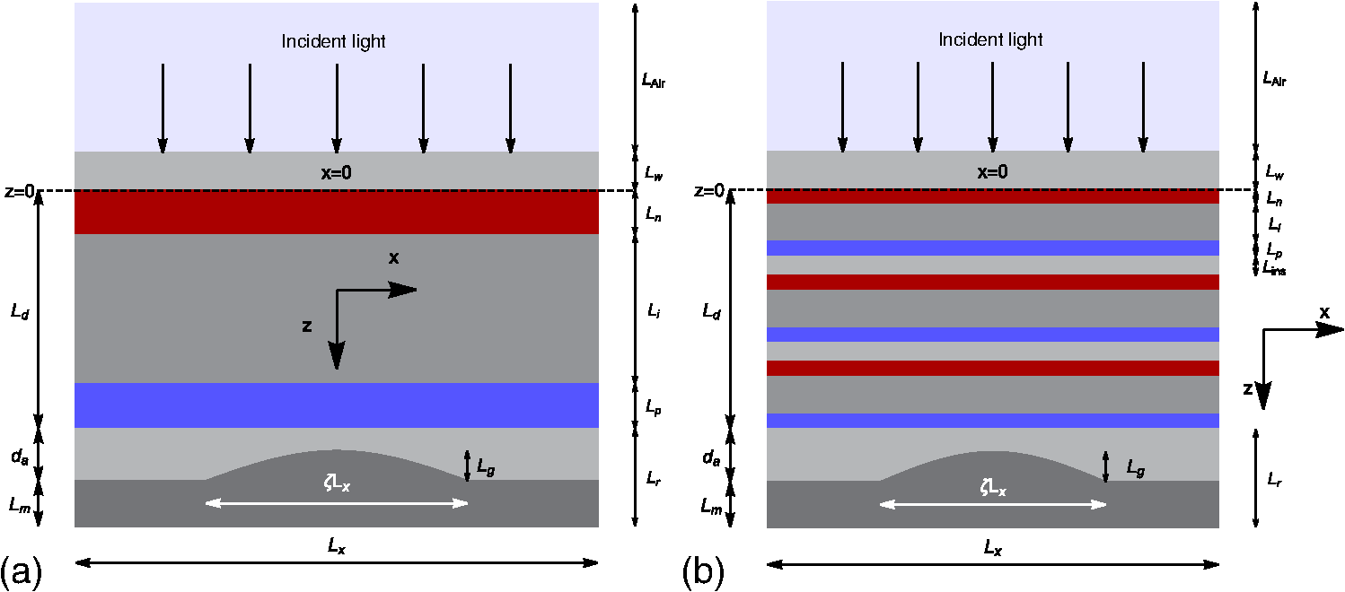 Fig. 2The average number of EHPs generated per incident photon, summed over the layer (solid black curve) and all semiconductor layers (dashed black curve), plotted against for a p-i-n junction solar cell with either (a) periodically corrugated back reflector or (b) flat reflector. The background is the photon flux density for AM1.5G spectrum is also shown. 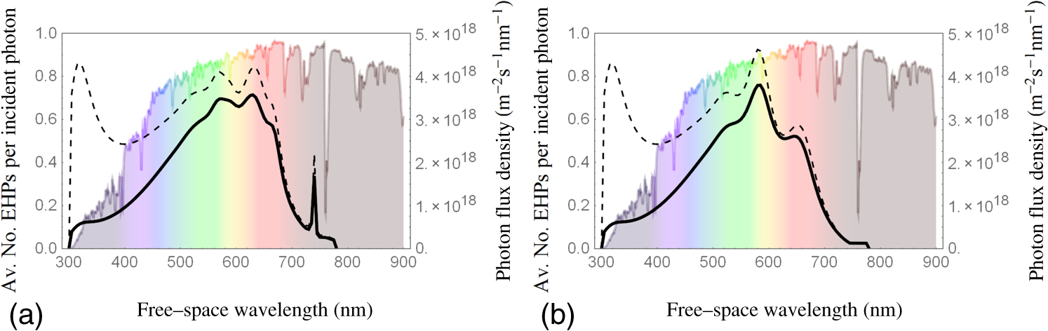 The EHP generation rate is mapped as a function of and in the unit cell for incident -polarized light and -polarized light in Fig. 3. Therein, the quoted values of the short-circuit optical current density are calculated assuming that every EHP created in the layer contributes to . This is necessarily larger than the short-circuit current density , which is the electronically simulated current density that flows when the solar cell is illuminated and no external bias is applied (i.e., when ). The generation rate for -polarized light is greater than that for -polarized light within the layer. This accounts for an increase in the short-circuit optical current density from for -polarized light to for -polarized light. Fig. 3EHP generation rate () as a function of and in the unit cell for incident (a) -polarized light and (b) -polarized light. The single p-i-n junction solar cell is described in Sec. 3.1. The and layers are lightly shaded and demarcated from the layer by dashed lines. The short-circuit optical current density is assumed to mainly originate from EHP generation in the layer. The values of quoted in the legends were calculated assuming that every EHP generated in the layer contributes to . 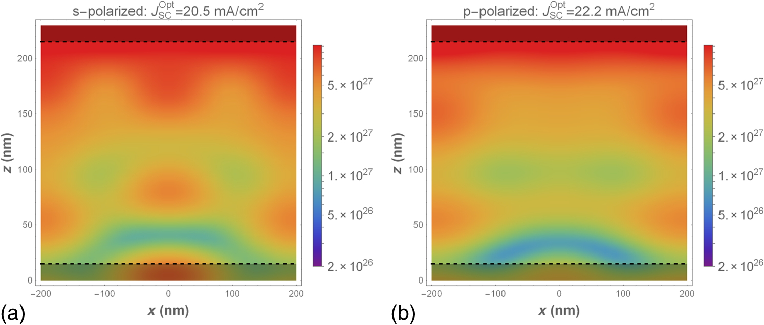 The maximum efficiency , that is, the maximum electrical power density producible by the solar cell divided by the of incident solar power density, of the single p-i-n junction solar cell for normally incident, unpolarized solar light, can be inferred from the plot provided in Fig. 4. The maximum efficiency is , which arises when the externally applied voltage is and the current density is (by convention, the plot shows the photoinduced current density in the fourth quadrant. Current densities quoted in the text and in tables are always positive when the device is producing electrical power.) This corresponds to a maximum power density of . Fig. 4plot for a single p-i-n junction solar cell with either a flat (dashed red curve) or a periodically corrugated (solid blue curve) black reflector, as described in Sec. 3.1. The normally incident solar light is unpolarized. The maximum efficiency is for the flat back reflector and for the periodically corrugated back reflector. The thin dotted lines mark the maximum power point of each cell. 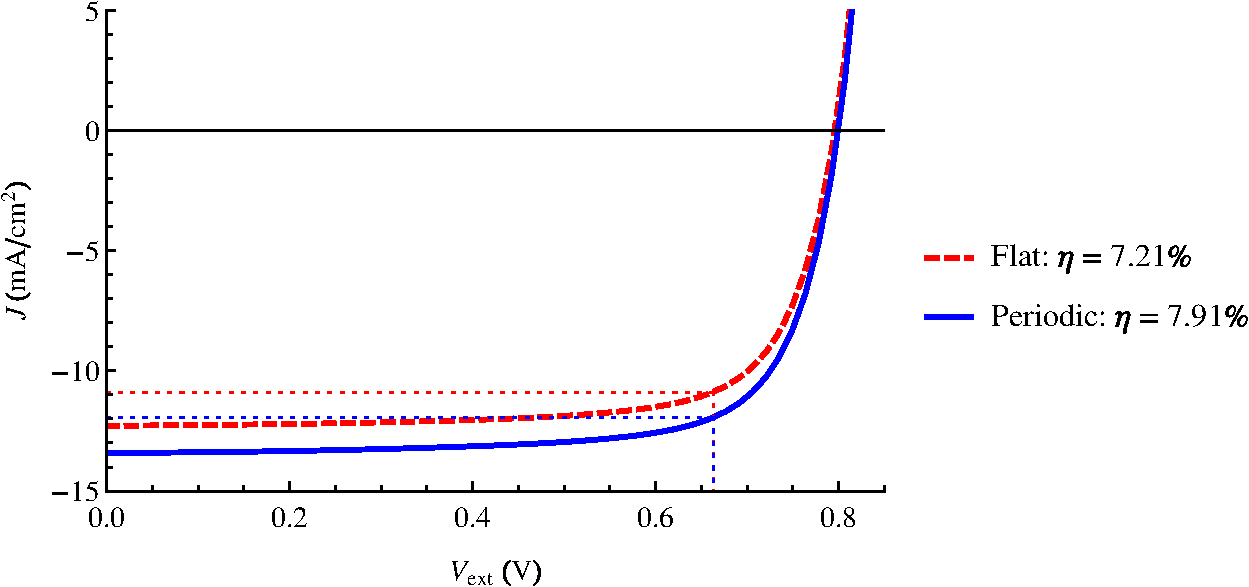 The fill factor (FF), that is, the ratio of the maximum power of the solar cell to the product of the short-circuit current and the open-circuit voltage, is a measure of the ideality of the solar cell. The FF of this cell is 0.738. These values are similar to those reported for other simulations46,47 as well as to those found experimentally.48 3.1.2.Flat back reflectorNow, we replace the periodically corrugated back reflector in Sec. 3.1.1 with a flat back reflector by setting . Figure 2(b) shows the absorption spectrum for this solar cell. More than 60% of the absorbed ultraviolet photons are absorbed in the layer, and so do not significantly contribute to the electrical current generated by the solar cell. The number of photons absorbed in the layer is lower than in the solar cell with the periodically corrugated back reflector considered in Sec. 3.1.1, with a noticeably smaller peak around 640 nm and a complete lack of a peak at 740 nm. The greater number of peaks in Fig. 2(a), as compared to Fig. 2(b), suggests that the periodically corrugated back reflector facilitates coupling between incident light and surface-plasmon-polariton waves or waveguide modes. However, a detailed analysis of the coupling to surface-plasmon-polariton waves and waveguide modes is a matter for future study. The maximum efficiency of the single p-i-n junction solar cell for normally incident, unpolarized solar light falls to , as may be inferred from the corresponding plot in Fig. 4. This arises when the externally applied voltage is , the same as in the solar cell with the periodically corrugated back reflector, but with a lower current density, . The FF is the same as that for the periodically corrugated back reflector. 3.2.Triple p-i-n Junction Solar CellNext, we turn to the simulation of a solar cell containing three p-i-n junctions. Each component junction, labeled , comprises a layer labeled , an layer labeled , and a layer labeled . Between the junctions and there is a thin AZO window labeled , of thickness ; likewise, between the junctions and , there is a thin AZO layer labeled , of thickness . The thicknesses of all layers, along with the corresponding bandgaps for the semiconductor layers, are listed in Table 3. Since our model does not support electron and hole tunneling, each junction is connected to an independent electrical circuit, which is efficacious for improved energy generation.5 Table 3Thicknesses, bandgaps, and doping densities for all layers in the triple p-i-n junction solar cell.
3.2.1.Periodically corrugated back reflectorWe begin with a back reflector, which is periodically corrugated,25 as in Eq. (1) and as schematically illustrated in Fig. 1(b). With regard to Eq. (1), we chose , , , , , and . As in Sec. 3.1, solar light was assumed to be normally incident. For unpolarized incident solar light, the average number of EHPs generated per incident photon, summed over all three layers (solid, black curve), is plotted against in Fig. 5(a). Also shown in the same figure is the spectrum of the average number of EHPs per incident photon generated in the entirety of the three p-i-n junctions (dashed, black curve). Notice that, compared to Fig. 2, absorption occurs much further into the infrared region of the spectrum, with significant peaks for . Fig. 5The average number of EHPs generated per incident photon, summed over all three layers (solid black curve) and all semiconductor layers (dashed black curve), plotted against for a triple p-i-n junction solar cell with either (a) periodically corrugated back reflector or (b) flat reflector. The background is the photon flux density for AM1.5G spectrum is also shown. 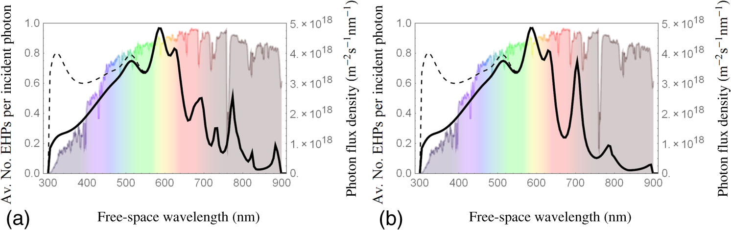 The EHP generation rate is mapped as a function of and in the unit cell for -polarized light and -polarized light in Fig. 6. The figure shows that the effect of the periodically corrugated back reflector is predominantly limited to the p-i-n junction closest to the reflector and that the difference between - and -polarized light is only significant in regions that are affected by the back reflector. Fig. 6EHP generation rate () as a function of and in the unit cell for incident (a) -polarized light and (b) -polarized light. The triple p-i-n junction solar cell is described in Sec. 3.2. The and layers and the AZO window are lightly shaded and demarcated from the layers by dashed lines. 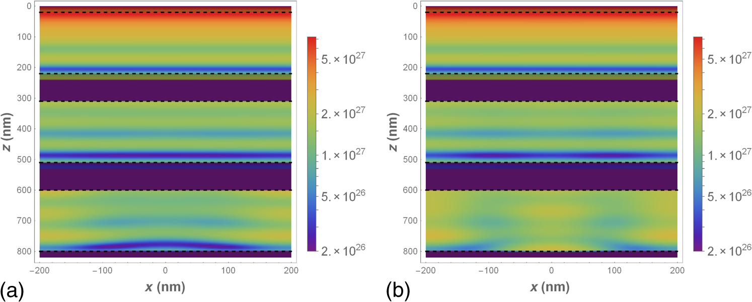 The corresponding values of , calculated assuming that every EHP generated in each layer contributes to , are presented in Table 4, along with the short-circuit current density , open-circuit voltage , FF, and efficiency . Table 4The short-circuit current density JSC, open-circuit voltage VOC, FF, efficiency η, and the optical short-circuit current density JSCOpt calculated with the assumption that every EHP generated in each i layer of the triple p-i-n junction contributes to JSCOpt. Results are presented for the cases for periodic back reflectors and flat back reflectors. For comparison, results are also presented for the single p-i-n junction solar cells described in Sec. 3.1, with periodic and flat back reflectors.
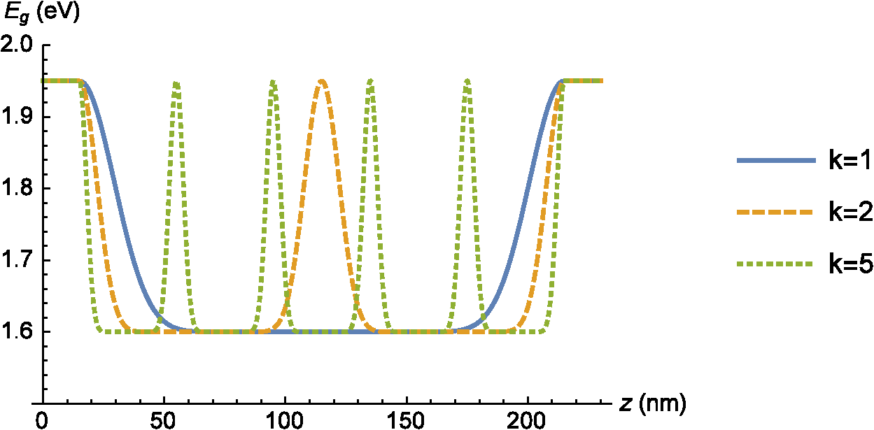
The maximum efficiency of the triple junction solar cell, for unpolarized incident solar light, may be inferred from the corresponding plot provided in Fig. 7. It is , which arises when the externally applied voltages in the ’th junction are , , and and the current densities in the ’th junction are , , and . These results correspond to a maximum power density of . The FFs, open circuit voltages, and short circuit currents are listed in Table 4. Fig. 7curves for each of the three p-i-n junctions in the triple p-i-n junction solar cell (described in Sec. 3.1) with the periodically corrugated back reflector. The normally incident solar light is unpolarized. The maximum efficiency is for the junction (solid blue curve), 1.43% for the junction (dashed green curve), and 0.77% for the junction (dot-dashed red curve). The total efficiency is therefore 8.33%. The thin dotted lines mark the maximum power point of each p-i-n junction. 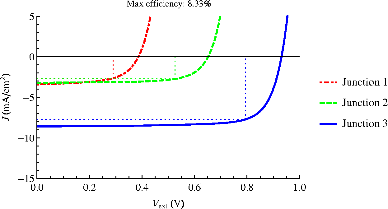 3.2.2.Flat back reflectorOur numerical studies reveal that changing from a periodically corrugated back reflector to a flat back reflector makes very little difference to the performance of the triple p-i-n junction solar cell considered here. Figures 5 and 7 suggest that this is because the influence of the periodically corrugated back reflector is masked by the relatively large optical thickness of the triple junction, especially for shorter wavelengths. Indeed, the differences between Figs. 5(a) and 5(b) are minimal at shorter wavelengths. For , the replacement of the periodically corrugated back reflector by its flat counterpart slightly reduces EHP generation, resulting in a decrease in efficiency from to , as shown in Table 4. The greater number of peaks in Fig. 5(a) as compared to Fig. 5(b) [e.g., the conspicuous peak at 740 nm in Fig. 5(a) is absent from Fig. 5(b)] suggests that the periodically corrugated back reflector facilitates coupling between incident light and surface-plasmon-polariton waves or waveguide modes. 4.Numerical Results for Nonhomogeneous LayersLet us turn now to solar cells with layers that are nonhomogeneous in the thickness direction. Only single p-i-n junction cells are considered here. We choose the same solar cell parameters as were used in Sec. 3.1.1, except that the thickness of the layer , and the layer bandgap (in eV) is varied as where is the minimum bandgap in the layer, is the amplitude of the perturbation from the homogeneous case (i.e., represents the case of a homogeneous layer), is a relative phase shift, is the number of periods of the perturbation, and is a shaping parameter. Note that, as in Ref. 49, for example, the bandgaps in the and layers are chosen to be relatively large (i.e., 1.95 eV), which minimizes optical absorption in these layers and, consequently, increases the generation rate of EHPs in the layer. We set , , , and . Figure 8 shows three example bandgap profiles for , , and . The choice results in profile peaks at the interfaces of the layer with the and the layers.The essential features of the principal effects of nonhomogeneity in the thickness direction can be initially studied by implementing a 1-D model for the electrical portion of the simulation. Accordingly, we average the 2-D EHP generation rate along the axis to form a 1-D EHP generation rate. In this section, we demonstrate the effect of varying both the amplitude of the bandgap profile and the layer thickness . Figure 9(a) shows the variation of the short-circuit current density with both , and . The maximum value of is , which occurs for and . Similarly, Fig. 9(b) shows the variation of the open-circuit voltage with both and . The maximum value of is 1.22 V, which occurs for and . Finally, Fig. 9(c) shows the variation of the FF with both and . The maximum value of FF is 0.73, which occurs for and . It is important to note here that and FF generally decrease with thickness of the p-i-n junction, while has an optimal thickness within the explored range. Fig. 9(a) The short-circuit current (), (b) open-circuit voltage (V), and (c) FF, plotted against amplitude , for for the single p-i-n junction solar cell with periodically nonhomogeneous layer described in Sec. 4. 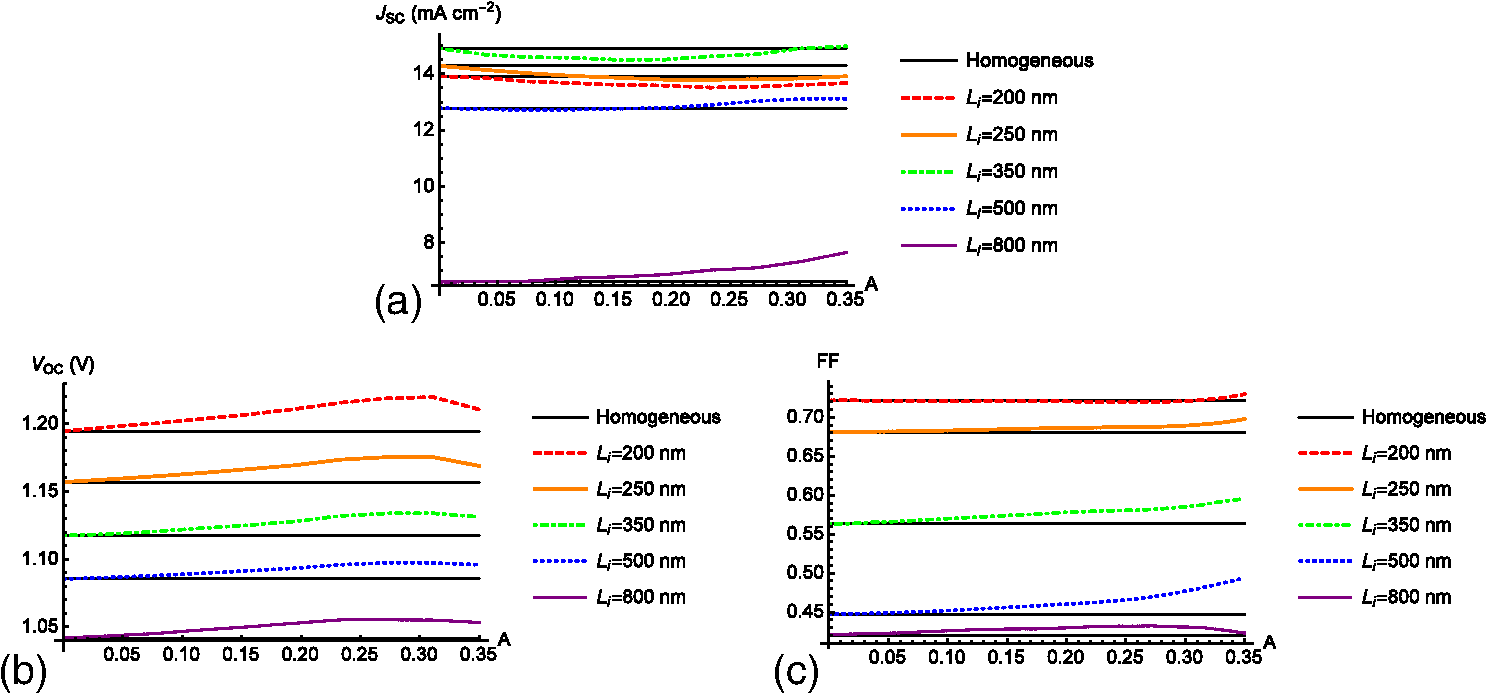 The optical efficiency is defined as the fraction of incident solar energy absorbed by the layer of the cell. In Fig. 10(a), the optical efficiency of the solar cell is plotted against amplitude for the layer thicknesses . At every value of , is greater at greater values of . Specifically, for solar cells with homogeneous layers, yields an optical efficiency of , while a cell with yields an optical efficiency of only . For each layer thickness, decreases as increases from zero and then reaches a local minimum before increasing as increases. Thicker cells are more positively affected by an increase in amplitude , with improving efficiency in cells with . Fig. 10Plots of (a) optical efficiency and (b) relative optical efficiency against amplitude for for the single p-i-n junction solar cell with periodically nonhomogeneous layer described in Sec. 4. The solid black lines allow comparisons with the corresponding homogeneous solar cells (i.e., solar cells with ). 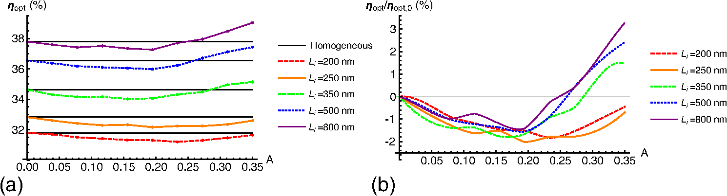 The relative optical efficiency is given by , where denotes the optical efficiency calculated with . That is, represents the optical efficiency of the corresponding solar cell with a homogeneous layer. Plots of versus are provided in Fig. 10(b). We see that for , a perturbation of any amplitude decreases efficiency, while for , maximal optical efficiency occurs for maximal . In Fig. 11(a), the total efficiency is plotted against for . At all values of , thinner cells are more efficient than thicker cells. The efficiency of thicker cells increases as the amplitude increases, with improving efficiency in cells with . All cells exhibit an improvement in efficiency for , although for thinner cells, the improvement is very modest. The maximum attained efficiency is for a cell with . The relative efficiency is given by , where denotes the efficiency calculated with . That is, represents the efficiency of the corresponding solar cell with a homogeneous layer. Plots of versus are provided in Fig. 11(b). These plots confirm that for all thicknesses, the greatest increase in efficiency compared to the corresponding homogeneous case (i.e., the case) occurs when . The greatest increase in relative efficiency, 18%, is observed for , where the cell efficiency increases from 3% to 3.5%. Fig. 11Plots of (a) total efficiency and (b) relative total efficiency against amplitude A for for the single p-i-n junction solar cell with periodically nonhomogeneous layer described in Sec. 4. The solid black lines allow comparisons with the corresponding homogeneous solar cells (i.e., solar cells with ). 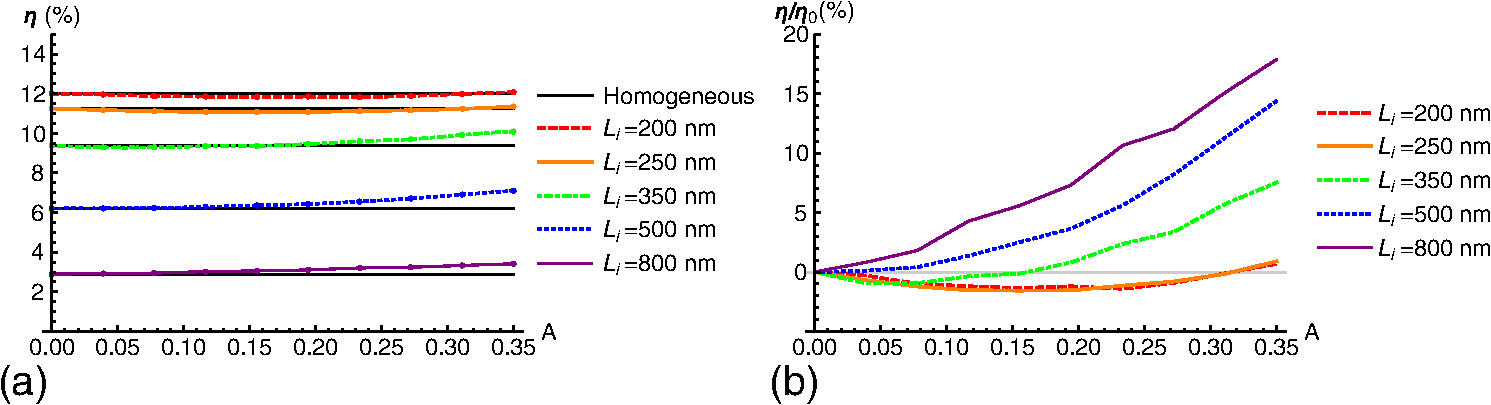 The electrical efficiency is defined as the ratio of total efficiency , as shown in Fig. 11, to optical efficiency , as shown in Fig. 10. In Fig. 12(a), the electrical efficiency is plotted against for the layer thicknesses . The electrical efficiency increases uniformly with increasing and with decreasing layer thickness. Specifically, at , an layer thickness gives rise to , while an layer thickness gives rise to . The relative electrical efficiency is given by , where denotes the electrical efficiency calculated with . That is, represents the electrical efficiency of the corresponding solar cell with a homogeneous layer. The plots in Fig. 12(b) of against confirm that the electrical efficiencies of cells with thicker layers are more strongly affected by an increase in amplitude and that the maximum electrical efficiencies are achieved at the largest values of . The efficiencies represented in Figs. 10Fig. 11–12 for and 0.35 are listed in Table 5, along with the corresponding values of , , and . Fig. 12Plots of (a) electrical efficiency and (b) relative electrical efficiency against amplitude A for for the single p-i-n junction solar cell with periodically nonhomogeneous layer described in Sec. 4. The solid black lines allow comparisons with the corresponding homogeneous solar cells (i.e., solar cells with ). 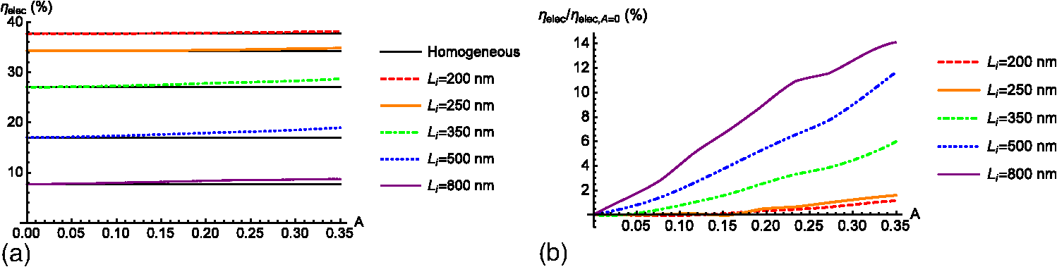 Table 5The short-circuit current density JSC, open-circuit voltage VOC, FF, efficiency η, optical efficiency ηopt, and electrical efficiency ηelec for single p-i-n junction cells with (i) homogeneous i layers of thickness Li∈{200,250,350,500,800} nm and (ii) nonhomogeneous i layers of the same thickness when A has been optimized for efficiency.
5.Closing RemarksA 2-D finite-element model was devised to simulate the combined optical and electrical performances of amorphous-silicon thin-film solar cells. Using this model, we have investigated the effects of
Our numerical experiments have demonstrated that by increasing the number of p-i-n junctions from one to three, the solar-cell efficiency may be increased. In this paper, we have shown a relative increase of 14% from the single p-i-n solar-cell with flat reflector at 7.2% to the triple p-i-n junction with flat reflector at 8.18%. The efficiency may be further increased by incorporating a periodically corrugated back reflector, as opposed to a flat back reflector. Also, by implementing a hybrid 2-D optical/1-D electrical model, we found that modest total efficiency gains (of up to 17% for solar cells) can be achieved via the judicious incorporation of periodic nonhomogeneity in the layer, particularly for thicker single p-i-n junction solar cells. A comparison of our results with those published in literature for similar types of solar cells shows that the former are in quite good agreement with the latter. This is demonstrated in Fig. 13, wherein efficiency is plotted as a function of the FF for the most efficient cells investigated here and for similar types of solar cells reported by other authors.34,46,48 For example, a 200-nm-thick single p-i-n junction solar cell (bandgap 1.78 eV) with a flat back reflector was shown to have an efficiency that increased to 7.25% when the flat reflector was replaced by a periodically corrugated back reflector in Ref. 46. Our model yielded for a 230-nm-thick single p-i-n junction solar cell with a flat back reflector that increased to for a periodically corrugated back reflector, the bandgap being 1.6 eV. These results are also close to the experimentally obtained with a 280-nm-thick single-junction solar cell (bandgap 1.75 eV).48 A 200-nm-thick solar cell with a bandgap of 1.75 eV and containing a dispersal of metal nanoparticles also has efficiency in the same range, that is, .34 Fig. 13Efficiency as a function of the FF of solar cells studied herein and in several publications, both theoretical and experimental, concerning similar types of solar cells by other authors.34,46,48 The maximum efficiency for a single-junction a-Si:H solar cell published to date49 is highlighted by the yellow star. The points without a superscript are for single-junction solar cells. For the points with a superscript, the superscript refers to the number of the junction in the triple p-i-n junction solar cell simulated. 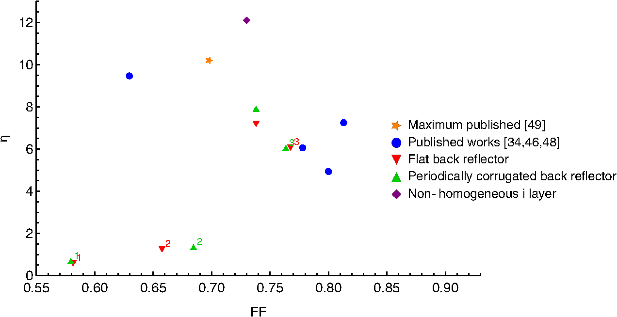 Let us also note that the FFs and efficiencies of the individual junctions within the triple p-i-n junction solar cell simulated by us are reasonable as well. The efficiency of the junction labeled is for a flat back reflector and for a periodically corrugated back reflector. As expected, the higher bandgap in this junction, compared to the simulated single p-i-n junction, results in a higher open-circuit voltage at the cost of a smaller short-circuit current density. The other two junctions have lower efficiency because their bandgaps are lower (1.58 and 1.39 eV), and they are shaded by the junction(s) closer to the AZO window. Our numerical findings vindicate the modeling approach undertaken wherein both the optical and electrical behaviors were simultaneously accommodated. Modeling only the optical behavior or only the electrical behavior is inadequate, as it is the coupling of these two behaviors that determines the overall efficiency of the solar cell. The development of the combined optical and electrical model and the preliminary numerical results presented herein pave the way for future wider-ranging parametric studies aimed at optimizing the design parameters of thin-film solar cells for maximum efficiency. We also expect to use this model to study thin-film photovoltaic solar cells made of materials other than amorphous silicon. AcknowledgmentsT. H. A. thanks the Charles Godfrey Binder Endowment for partial financial support during a six-month stay at the Pennsylvania State University. T. G. M. acknowledges the support of EPSRC grant EP/M018075/1. A. L. thanks the National Science Foundation for partial financial support under Grant No. DMR-1125591, and he is grateful to the Charles Godfrey Binder Endowment at Penn State for ongoing support of his research. This manuscript is an extension of the conference paper: T. H. Anderson, M. Faryad, T. G. Mackay, A. Lakhtakia, and R. Singh, “Combined optical-electrical finite-element simulations of thin-film solar cells—preliminary results,” Proc. SPIE 9561, 956102 (2015). ReferencesM. Osborne,
“Big picture: 318 GW of solar modules to be installed in next 5 years says HIS,”
(2015) http://pv-tech.org/news/big_picture_318gw_of_solar_modules_to_be_installed_in_next_5_years_says_his July 2015). Google Scholar
J. M. Martnez-Duart and J. Hernández-Moro,
“Photovoltaics firmly moving to the terawatt scale,”
J. Nanophotonics, 7 078599
(2013). http://dx.doi.org/10.1117/1.JNP.7.078599 1934-2608 Google Scholar
R. Singh,
“Why silicon is and will remain the dominant photovoltaic material,”
J. Nanophotonics, 3 032503
(2009). http://dx.doi.org/10.1117/1.3196882 1934-2608 Google Scholar
A. A. Asif, R. Singh and G. F. Alapatt,
“Technical and economic assessment of perovskite solar cells for large scale manufacturing,”
J. Renewable Sustainable Energy, 7 043120
(2015). http://dx.doi.org/10.1063/1.4927329 Google Scholar
R. Singh, G. F. Alapatt and A. Lakhtakia,
“Making solar cells a reality in every home: opportunities and challenges for photovoltaic device design,”
IEEE J. Electron Devices Soc., 1 129
–144
(2013). http://dx.doi.org/10.1109/JEDS.2013.2280887 Google Scholar
P. Verlinden et al.,
“The surface texturization of solar cells: a new method with V-grooves with controllable sidewall angles,”
Sol. Energy Mater. Sol. Cells, 26 71
–78
(1992). http://dx.doi.org/10.1016/0927-0248(92)90126-A SEMCEQ 0927-0248 Google Scholar
N. Yamada et al.,
“Characterization of antireflection moth-eye film on crystalline silicon photovoltaic module,”
Opt. Express, 19 A118
–A125
(2011). http://dx.doi.org/10.1364/OE.19.00A118 OPEXFF 1094-4087 Google Scholar
P. Sheng, A. N. Bloch and R. S. Stepleman,
“Wavelength-selective absorption enhancement in thin-film solar cells,”
Appl. Phys. Lett., 43 579
–581
(1983). http://dx.doi.org/10.1063/1.94432 APPLAB 0003-6951 Google Scholar
C. Heine and R. F. Morf,
“Submicrometer gratings for solar energy applications,”
Appl. Opt., 34 2476
–2482
(1995). http://dx.doi.org/10.1364/AO.34.002476 APOPAI 0003-6935 Google Scholar
M. Solano et al.,
“Optimization of the absorption efficiency of an amorphous-silicon thin-film tandem solar cell backed by a metallic surface-relief grating,”
Appl. Opt., 52 966
–979
(2013). http://dx.doi.org/10.1364/AO.52.000966 APOPAI 0003-6935 Google Scholar
S. K. Dhungel et al.,
“Double-layer antireflection coating of for crystalline silicon solar cells,”
J. Korean Phys. Soc., 49 885
–889
(2006). KPSJAS 0374-4884 Google Scholar
S. A. Boden and D. M. Bagnall,
“Sunrise to sunset optimization of thin film antireflective coatings for encapsulated, planar silicon solar cells,”
Prog. Photovoltaics Res. Appl., 17 241
–252
(2009). http://dx.doi.org/10.1002/pip.v17:4 PPHOED 1062-7995 Google Scholar
D. M. Schaadt, B. Feng and E. T. Yu,
“Enhanced semiconductor optical absorption via surface plasmon excitation in metal nanoparticles,”
Appl. Phys. Lett., 86 063106
(2005). http://dx.doi.org/10.1063/1.1855423 APPLAB 0003-6951 Google Scholar
S. Pillai et al.,
“Surface plasmon enhanced silicon solar cells,”
J. Appl. Phys., 101 093105
(2007). http://dx.doi.org/10.1063/1.2734885 JAPIAU 0021-8979 Google Scholar
J.-Y. Lee and P. Peumans,
“The origin of enhanced optical absorption in solar cells with metal nanoparticles embedded in the active layer,”
Opt. Express, 18 10078
–10087
(2010). http://dx.doi.org/10.1364/OE.18.010078 OPEXFF 1094-4087 Google Scholar
R. A. Sinton et al.,
“27.5-percent silicon concentrator solar cells,”
IEEE Electron Device Lett., 7 567
–569
(1986). http://dx.doi.org/10.1109/EDL.1986.26476 EDLEDZ 0741-3106 Google Scholar
K. Nishioka et al.,
“Evaluation of InGaP/InGaAs/Ge triple-junction solar cell and optimization of solar cells structure focusing on series resistance for high-efficiency concentrator photovoltaic systems,”
Sol. Energy Mater. Sol. Cells, 90 1308
–1321
(2006). http://dx.doi.org/10.1016/j.solmat.2005.08.003 SEMCEQ 0927-0248 Google Scholar
M. E. Solano et al.,
“Buffer layer between a planar optical concentrator and a solar cell,”
AIP Adv., 5 097150
(2015). http://dx.doi.org/10.1063/1.4931386 AAIDBI 2158-3226 Google Scholar
L. Liu et al.,
“Experimental excitation of multiple surface-plasmon-polariton waves and waveguide modes in a one-dimensional photonic crystal atop a two-dimensional metal grating,”
J. Nanophotonics, 9 093593
(2015). http://dx.doi.org/10.1117/1.JNP.9.093593 1934-2608 Google Scholar
L. M. Anderson,
“Parallel-processing with surface plasmons, a new strategy for converting the broad solar spectrum,”
in Proc. 16th IEEE Photovoltaic Specialists Conf.,
371
–377
(1982). Google Scholar
L. M. Anderson,
“Harnessing surface plasmons for solar energy conversion,”
Proc. SPIE, 408 172
–178
(1983). http://dx.doi.org/10.1117/12.935723 PSISDG 0277-786X Google Scholar
Jr. J. A. Polo, T. G. Mackay and A. Lakhtakia, Electromagnetic Surface Waves: A Modern Perspective, Elsevier, Waltham, Massachusetts
(2013). Google Scholar
T. Khaleque and R. Magnusson,
“Light management through guided-mode resonances in thin-film silicon solar cells,”
J. Nanophotonics, 8 083995
(2014). http://dx.doi.org/10.1117/1.JNP.8.083995 1934-2608 Google Scholar
A. De Vos,
“Detailed balance limit of the efficiency of tandem solar cells,”
J. Phys. D: Appl. Phys., 13 839
–846
(1980). http://dx.doi.org/10.1088/0022-3727/13/5/018 JPAPBE 0022-3727 Google Scholar
M. Faryad and A. Lakhtakia,
“Enhancement of light absorption efficiency of amorphous-silicon thin-film tandem solar cell due to multiple surface-plasmon-polariton waves in the near-infrared spectral regime,”
Opt. Eng., 52 087106
(2013). http://dx.doi.org/10.1117/1.OE.52.8.087106 Google Scholar
M. I. Kabir et al.,
“Amorphous silicon single-junction thin-film solar cell exceeding 10% efficiency by design optimization,”
Int. J. Photoenergy, 2012 460919
(2012). http://dx.doi.org/10.1155/2012/460919 Google Scholar
S. M. Iftiquar et al.,
“Single- and multiple-junction p-i-n type amorphous silicon solar cells with and nc-Si:H films,”
Photodiodes—From Fundamentals to Applications,
(2012) http://www.intechopen.com/books/photodiodes-from-fundamentals-to-applications/single-and-multiple-junction-p-i-n-type-amorphous-silicon-solar-cells-with-p-a-si1-xcx-h-and-nc-si-h Google Scholar
J. Nelson, The Physics of Solar Cells, Imperial College Press, London, United Kingdom
(2003). Google Scholar
S. J. Fonash, Solar Cell Device Physics, 2nd ed.Academic Press, Burlington, Massachusetts
(2010). Google Scholar
M. Faryad et al.,
“Optical and electrical modeling of an amorphous-silicon tandem solar cell with nonhomogeneous intrinsic layers and a periodically corrugated back-reflector,”
Proc. SPIE, 8823 882306
(2013). http://dx.doi.org/10.1117/12.2024712 PSISDG 0277-786X Google Scholar
E. Schroten et al.,
“Simulation of hydrogenated amorphous silicon germanium alloys for bandgap grading,”
MRS Proc., 557 773
–778
(1999). http://dx.doi.org/10.1557/PROC-557-773 MRSPDH 0272-9172 Google Scholar
T. H. Anderson et al.,
“Towards numerical simulation of nonhomogeneous thin-film silicon solar cells,”
Proc. SPIE, 8981 898115
(2014). http://dx.doi.org/10.1117/12.2041663 PSISDG 0277-786X Google Scholar
“Reference solar spectral irradiance: air mass 1.5,”
(2015) http://rredc.nrel.gov/solar/spectra/am1.5/ July ). 2015). Google Scholar
K. K. Gandhi et al.,
“Simultaneous optical and electrical modeling of plasmonic light trapping in thin-film amorphous silicon photovoltaic devices,”
J. Photonics Energy, 5 057007
(2015). http://dx.doi.org/10.1117/1.JPE.5.057007 Google Scholar
R. A. Street, Hydrogenated Amorphous Silicon, 1st ed.Cambridge University Press, Cambridge, United Kingdom
(1991). Google Scholar
A. Zangwill, Modern Electrodynamics, Cambridge University Press, New York, New York
(2013). Google Scholar
A. S. Ferlauto et al.,
“Analytical model for the optical functions of amorphous semiconductors from the near-infrared to ultraviolet: Applications in thin film photovoltaics,”
J. Appl. Phys., 92 2424
–2436
(2002). http://dx.doi.org/10.1063/1.1497462 JAPIAU 0021-8979 Google Scholar
M. Nawaz,
“Computer analysis of thin-film amorphous silicon heterojunction solar cells,”
J. Phys. D: Appl. Phys., 44 145105
(2011). http://dx.doi.org/10.1088/0022-3727/44/14/145105 JPAPBE 0022-3727 Google Scholar
S. R. Dhariwal and S. Rajvanshi,
“Theory of amorphous silicon solar cell (a): numerical analysis,”
Sol. Energy Mater. Sol. Cells, 79 199
–213
(2003). http://dx.doi.org/10.1016/S0927-0248(02)00414-2 SEMCEQ 0927-0248 Google Scholar
A. Fantoni, M. Viera and R. Martins,
“Influence of the intrinsic layer characteristics on a-Si:H p-i-n solar cell performance analysed by means of a computer simulation,”
Sol. Energy Mater. Sol. Cells, 73 151
–162
(2002). http://dx.doi.org/10.1016/S0927-0248(01)00120-9 SEMCEQ 0927-0248 Google Scholar
R. Chavali et al.,
“Multiprobe characterization of inversion charge for self-consistent parameterization of HIT cells,”
IEEE J. Photovoltaics, 5 725
–735
(2015). http://dx.doi.org/10.1109/JPHOTOV.2014.2388072 IJPEG8 2156-3381 Google Scholar
M. Zeman et al.,
“Device modeling of a-Si:H alloy solar cells: calibration procedure for determination of model input parameters,”
MRS Proc., 507 409
–414
(1998). http://dx.doi.org/10.1557/PROC-507-409 MRSPDH 0272-9172 Google Scholar
X. Y. Gao, Y. Liang and Q. G. Lin,
“Analysis of the optical constants of aluminum-doped zinc-oxide films by using the single-oscillator model,”
J. Korean Phys. Soc., 57 710
–714
(2010). http://dx.doi.org/10.3938/jkps.57.710 KPSJAS 0374-4884 Google Scholar
Handbook of Optical Constants of Solids, Academic Press, Boston, Massachusetts
(1985). Google Scholar
M. G. Deceglie et al.,
“Design of nanostructured solar cells using coupled optical and electrical modeling,”
Nano Lett., 12 2894
–2900
(2012). http://dx.doi.org/10.1021/nl300483y NALEFD 1530-6984 Google Scholar
C. Lee et al.,
“Two-dimensional computer modeling of single junction a-Si:H solar cells,”
in Proc. 34th IEEE Photovoltaic Specialists Conf.,
001118
–001122
(2009). http://dx.doi.org/10.1109/PVSC.2009.5411215 Google Scholar
J. Meier et al.,
“Potential of amorphous and microcrystalline silicon solar cells,”
Thin Solid Films, 451–452 518
–524
(2004). http://dx.doi.org/10.1016/j.tsf.2003.11.014 THSFAP 0040-6090 Google Scholar
T. Matsui et al.,
“Development of highly stable and efficient amorphous silicon based solar cells,”
in Proc. 28th Eur. Photovoltaic Solar Energy Conf.,
2213
–2217
(2013). Google Scholar
BiographyTom H. Anderson received his BSc in mathematics and physics from the University of Edinburgh in 2011. He then received his MSc in fusion energy from the University of York in 2012. He is currently an applied mathematics PhD candidate at the University of Edinburgh. His research interests include the optical and electrical modeling of thin-film solar cells. Muhammad Faryad received his MSc (2006) and MPhil (2008) degrees in electronics from Quaid-i-Azam University and his PhD (2012) in engineering science and mechanics from Pennsylvania State University, where he served as a postdoctoral research scholar from 2012 to 2014. Currently, he is an assistant professor of physics at the Lahore University of Management Sciences. His research interests include modeling of thin-film solar cells, electromagnetic surface waves, photonic crystals, and sculptured thin films. Tom G. Mackay is a reader in the School of Mathematics at the University of Edinburgh and an adjunct professor in the Department of Engineering Science and Mechanics at the Pennsylvania State University. He is a graduate of the Universities of Edinburgh, Glasgow, and Strathclyde and a fellow of the Institute of Physics (United Kingdom) and SPIE. His research interests include the electromagnetic theory of novel and complex materials, including homogenized composite materials. Akhlesh Lakhtakia received his degrees from the Banaras Hindu University and the University of Utah. He is the Charles Godfrey Binder professor of engineering science and mechanics at the Pennsylvania State University. His current research interests include nanotechnology, bioreplication, forensic science, solar-energy harvesting, surface multiplasmonics, metamaterials, mimumes, and sculptured thin films. He is a fellow of OSA, SPIE, IoP, AAAS, APS, and IEEE. He received the 2010 SPIE technical achievement award. Rajendra Singh is D. Houser Banks professor at Clemson University. From solar cells to low power electronics, he has led the work on semiconductor and photovoltaic device materials and processing by manufacturable innovation and defining critical path. He has received a number of international awards. He was honored by U.S. President Barack Obama as a White House “Champion of Change for Solar Deployment” for his leadership in advancing solar energy with PV technology. |