
|
|
1.IntroductionOrganic light-emitting diodes (OLEDs) have attracted considerable research interest due to their broad applications in the next-generation flat-panel displays and eco-friendly solid-state lightings.1–4 In the past few decades, significant efforts have been devoted to maximize device efficiency through new materials combined with innovation in device structures, such as the development of phosphorescent emitters,5,6 thermally activated delayed fluorescent emitters,7,8 guest–host structure,9,10 cohost structure,11,12 p-i-n structure,3,13 and a simple device architecture,14 etc. So far, OLEDs have reached efficiencies on par with the traditional inorganic light-emitting diodes.4 OLED operation involves several steps: injection and transport of charge carriers, formation of tightly bound electron–hole pairs known as excitons, and radiative recombination of excitons. In general, the lowest theoretical voltage for running an OLED is at best equal to the energy gap between the highest occupied molecular orbital (HOMO) and the lowest unoccupied molecular orbital (LUMO) of the emitter molecule. Due to a poor electrical conductivity of organic molecules, operating voltages for most OLEDs are much higher than the HOMO–LUMO energy gaps of the emitter molecules. To reduce the operating voltages of OLEDs, -type- and -type-doped hole transport layer (HTL) and electron transport layer (ETL) are used.15,16 Even in the most advanced OLEDs, however, operating voltages are still higher than or close to the HOMO–LUMO energy gaps of emitter molecules.1,3,14 Recently, a new type of OLED involving ballistic Auger-electron injection at organic heterojunctions has been developed. This type of OLED has operating voltages well below the HOMO–LUMO energy gaps of the emitter molecules; i.e., the output photon energies are higher than the input electrical energies.17–21 In this report, we provide a review on the electronic processes at organic heterojunctions and Auger-electron-stimulated ultralow-voltage OLEDs. 2.Exciton Formation at HeterojunctionsToday, state-of-the-art OLEDs consist of a stack of many different functional organic layers to ensure effective charge injection, charge transport, and formation of excitons at a particular heterojunction. Figure 1(a) shows a simple bilayer heterojunction device, which includes an anode, a HTL, an ETL, and a cathode. Fig. 1(a) A simple bilayer device with an organic heterojunction. (b) The corresponding energy level diagram at equilibrium where holes and electrons are injected from their respective electrodes and accumulated at HTL/ETL interface to form excitons. 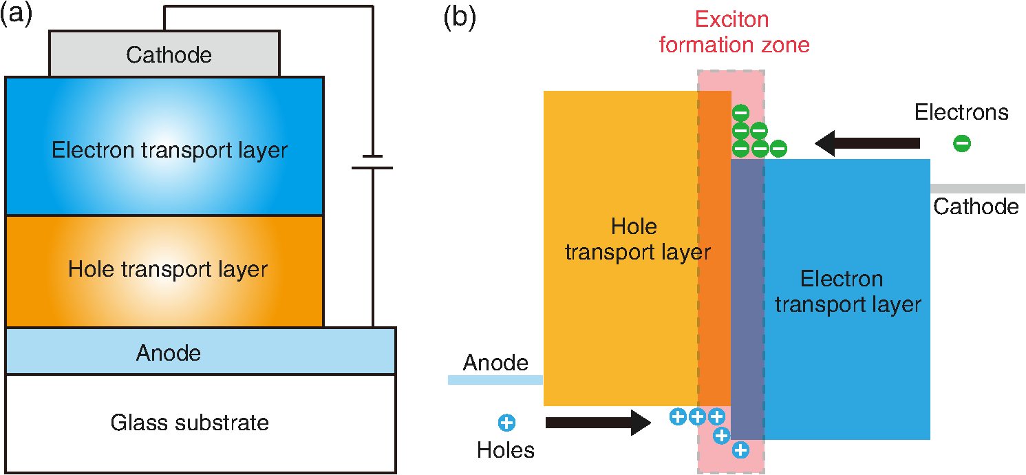 Under an external electrical bias, as shown in Fig. 1(b), the injected holes and electrons hop through the HOMO of the HTL and the LUMO of the ETL, respectively. When both holes and electrons reach the HTL/ETL interface, they may form excitons or continue hopping transport through the interface. In the case of a low energy offset at the heterojunction, charges will hop through the heterojunction and form exciton in either HTL or ETL. Figure 2(a) illustrates the case of exciton formation in both HTL and ETL sides of a heterojunction where HOMO and LUMO offsets are low. The exciton is generally formed within one molecule, and is often referred to as a Frenkel exciton.22 Fig. 2Schematic diagram of (a) Frenkel exciton and (b) CT exciton formation at an organic heterojunction. 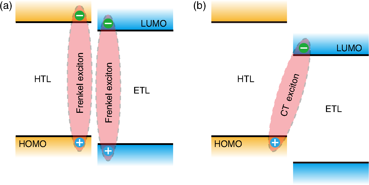 In the case of a large energy barrier at the interface, charges will accumulate at the HTL/ETL interface. This leads to the formation of excitons between holes on the HTL side and electrons on the ETL side. This type of exciton is referred to as a charge transfer (CT) exciton,22,23 as shown in Fig. 2(b). In recent years, CT excitons have been demonstrated to play a very important role in the performance of OLEDs. 3.Charge Transfer Excitons RecombinationOnce the CT excitons have been formed, the charges will recombine either radiatively or nonradiatively, depending on the time constant of a particular process. A decay process that occurs more quickly will be able to better compete against alternate processes and will thus occur more readily. 3.1.Radiative Recombination3.1.1.Exciplex emissionThe radiative recombination of CT excitons is known as exciplex emission, as shown in Fig. 3(a). Exciplex emission always shows a long wavelength and a broad spectrum because a small energy difference between the HOMO of HTL and the LUMO of ETL. In addition, exciplex emission is radiative recombination of singlet CT excitons and therefore generally exhibits low efficiency.24,25 Fig. 3(a) Schematic diagram of exciplex emission at the NPB/B4PyPPM heterojunction device. (b) Plot of the exciplex emission peak versus the energy difference between the LUMO of acceptor and the HOMO of donor for HTL/B4PyPPM heterojunction devices. Error bars represent range of the donor HOMOs reported in literature.21  Due to a large separation distance between the electrons and holes, CT excitons have been demonstrated recently to have a very small singlet–triplet energy splitting, which enables an efficient transition from nonradiative triplet states to radiative singlet states via a reverse-intersystem-crossing (RISC) process.26,27 Therefore, fluorescent OLEDs based on exciplex emission can harvest both singlet and triplet excitons through prompt and delayed fluorescent decay channels. Indeed, a high external quantum efficiency (EQE) () fluorescent OLED based on exciplex emission has been reported recently by mixing a hole transporting material with a bipolar host material to form CT excitons.28 Recently, a simple heterojunction device with a stack of -type HTL and an -type ETL also has been shown to yield an efficient () exciplex emission.29 It is known that the energy of exciton is lower than the energy difference in the unbound electron and hole pair. That is, the energy of exciplex emission, which originates from direct radiative recombination of CT excitons, should be lower than the energy difference between the HOMO of HTL and the LUMO of ETL. As shown in Fig. 3(b), however, the actual energies of exciplex emission are higher than the energy differences between the HOMOs of HTLs and the LUMOs of ETLs. Empirically, the exciplex emission energy can be expressed as follows:21 where is the LUMO of acceptor (ETL), is the HOMO of donor (HTL), and the constant is , which is comparable to a reported value measured from exciplex emission in solution.303.1.2.Energy transferFor a guest–host device, CT excitons can transfer their energies to chromophores when the excitonic energies of chromophores on either side of heterojunction are lower than that of the interfacial CT excitons.31,32 The excitons on the chromophores will recombine radiatively. As shown in Fig. 4, there are two mechanisms through which CT excitons can transfer energy to dopants: Förster energy transfer and Dexter energy transfer. Förster energy transfer is also called resonance energy transfer, which occurs through the Coulombic dipole–dipole interaction. In this case, an exciton generated on a donor molecule recombines to the ground state and transfers its energy to excite an acceptor. Förster energy transfer is a long-range process and mainly emerges between the two singlet excitons. The rate of Förster energy transfer is given by33 where is the distance between donor and acceptor, is the natural lifetime of the exciton, is the Förster radius, which describes the critical transfer distance that excitation transfer and spontaneous deactivation of the donor are of equal probability, and is given by the equation33 where is the Avogadro’s number, is the dipole orientation factor, is the fluorescent quantum yield of the donor, is the index of refraction of the medium containing the donor and acceptor, and is the overlap integral of the normalized donor emission spectrum and acceptor absorption spectrum.Dexter energy transfer is through exciton hopping, which involves electron hopping from a donor’s LUMO to an acceptor’s LUMO and electron hopping from the acceptor’s HOMO to the donor’s HOMO. Dexter energy transfer occurs within a short distance due to its overlap requirement of the wavefunction between the donor and acceptor. The rate constant for Dexter energy transfer is given by34 where describes specific orbital interactions and is the van der Waals radii of the donor and acceptor.These energy transfer mechanisms have been demonstrated to be a successful strategy for producing high-efficiency OLEDs. For a phosphorescent dopant, both singlet and triplet of CT excitons transfer energy to the phosphorescent dopant via Förster and Dexter processes, and then the singlets of phosphorescent dopant convert quickly into triplets via an efficient intersystem crossing (ISC). Therefore, both singlet and triplet of CT excitons can excite phosphorescent dopant yielding possibly 100% internal quantum efficiency. Indeed, high EQEs of 29.5%, 32.3%, and 35.6% for blue, green, red phosphorescent OLEDs, respectively, have been reported through effective use of the Förster and Dexter energy transfer from CT excitons that are formed by mixing HTL and ETL as a cohost.35–37 In the case of fluorescent dopants, both Förster and Dexter energy transfer also occur as well, also producing singlet and triplet excitons on the fluorescent dopant. But only singlet excitons can be used for light emission, triplet excitons decay by nonradiative transitions. Therefore, fluorescent-doped devices in general show a low efficiency. It is worth noting that shown in Fig. 4, however, triplet of CT excitons may upconvert into singlet of CT excitons via RISC process and then transfer to singlets of dopant via Förster energy transfer channel before it transfer to triplet of dopants through Dexter energy transfer process. Indeed, a high-efficiency () fluorescent-dopant-based OLED has been achieved recently by using an extremely low dopant concentration to minimize Dexter energy transfer from the triplet of CT excitons to triplet of fluorescent dopant.38 3.2.Nonradiative Recombination3.2.1.Phonon emissionIn addition to the radiative recombination pathways, CT excitons may decay nonradiatively via phonon emission. In fact, nonradiative recombination is a common process in semiconductor devices. CT excitons may recombine nonradiatively following an energy-gap law, which describes the rate of nonradiative decay increases exponentially with decreasing difference in energy between the ground and excited states. The rate constant for nonradiative decay is given by39 where is the energy of excited state, and are the constants related to phonon.Indeed, an extremely high nonradiative recombination of CT excitons has been demonstrated for heterojunction recently.40 As shown in Fig. 5(a), a unique energy level alignment and a large energy barrier lead to electrons and holes accumulation at interface and form CT excitons, which recombine nonradiatively by phonon emission at a very fast rate. This extremely fast CT excitons recombination makes heterojunction behave like an ideal Ohmic contact and thus leads to a very high rectifying characteristics from the electrode/organic contacts [see Fig. 5(b)]. Fig. 5(a) Schematic diagram of the CT excitons recombination by phonon emission at heterojunction. (b) The current density–voltage characteristics of the heterojunction device.40 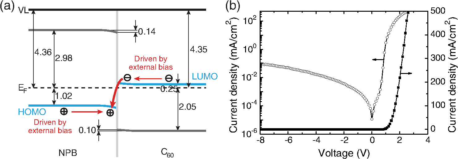 3.2.2.Auger recombinationThe CT exciton recombination may take another nonradiative pathway to release its energy by exciting an adjacent electron to higher energy states.17–21 This process is referred to as Auger recombination. Auger recombination is a common electronic process in inorganic semiconductors and quantum dots, in particular when the carrier concentration is high.41,42 In organic semiconductors, Auger recombination may involve bimolecular recombination, which CT excitons recombine at the heterojunction interface by transferring their energy to excite adjacent electrons to higher energy levels.22 As shown in Fig. 6, there are two possible types of Auger recombination at organic heterojunctions: (i) biexciton Auger recombination, where a ground-state biexciton decay into an excited state mono-exciton; (ii) negative trion Auger recombination, where a three-bound-particle (one hole and two electrons, i.e., charged exciton) state decay into one excited electron. The trion states were predicted theoretically and have been observed experimentally in other types of semiconductors such as quantum dots and quantum wells.43,44 Moreover, the trion was observed in carbon nanotubes with a large energy separation (0.1 to 0.2 eV) from the bright excitons.45 This value is consistent with the 0.22 eV energy difference between Auger recombination and exciplex emission at NPB/B4PyPPM heterojunction device.21 The Auger recombination rate at organic heterojunctions is given by21 where is the coefficient of Auger recombination, and are the concentration of electron and hole, respectively.Fig. 6Schematic illustration of possible types of Auger processes at an organic heterojunction: (a) biexciton Auger recombination and (b) negative trion Auger recombination.  Figure 7 shows a schematic energy diagram of negative trion Auger recombination at an organic heterojunction. The CT exciton recombination at a heterojunction interface releases its energy to excite a LUMO electron to higher energy states. This electron on a high energy state may either relax down a lower energy state via inelastic collisions or ballistically injects into the LUMO of donor. The energy offset condition for Auger-electron injection is given as20 where is the HOMO–LUMO energy gap of donor, and are the LUMO of acceptor and donor, respectively. Under this condition, the turn-on voltage of OLED for Auger-electron injections is no longer limited by the energy gap of the emitter molecule. The lowest possible turn-on voltage is20 where is the LUMO of acceptor and is the HOMO of donor.Fig. 7Schematic energy diagrams illustrating negative trion Auger recombination at an organic heterojunction.20  4.Ultralow Voltage Organic Light-Emitting Diodes through Auger-Electron Injection4.1.Bilayer Device StructuresFor negative trion Auger recombination at organic heterojunctions, a considerable energy offsets between the HOMOs and LUMOs of HTL and ETL are required to accumulate the amount of electrons and holes at the interface. Hence, Auger recombination is generally observed at heterojunctions where the ETLs have a deep energy level. Figure 8(a) shows the luminance-voltage characteristics of and Rubrene/B4PyPPM heterojunction devices, which have a turn-on voltage (defined as luminance at ) at 0.9 and 1.9 V, respectively. Clearly, these voltages are significantly lower than the HOMO–LUMO energy gap of Rubrene (2.2 eV). Fig. 8(a) Luminance-voltage characteristics and (b) schematic working mechanism of Rubrene/ETL heterojunction devices through Auger-electron injection. The inset in (a) is the EL spectra of the corresponding devices.20  The working mechanism of these ultralow operating voltages is related to negative trion Auger recombination at heterojunction interfaces. As shown in Fig. 8(b), there are three electronic processes at the Rubrene/ETLs heterojunction. Under a bias voltage, electrons in ETLs and holes in Rubrene drift toward the heterojunction. Owing to large energy offsets in both the HOMOs and LUMOs, electrons and holes accumulate at the interface leading to a negative trion Auger recombination [denoted as process I in Fig. 8(b)]. These Auger-electrons are ballistically injected into the LUMO of Rubrene [process II in Fig. 8(b)]. The injected Auger-electrons recombine with holes in the Rubrene layer to emit photons [process III in Fig. 8(b)]. The Auger-electrons overcome the energy barrier at the HTL/ETL heterojunctions, thus turn-on voltages of OLEDs with Auger-electron injection far below the energy gap of the emitter. It is worth noting that triplet–triplet annihilation (TTA) process has also been proposed to explain the ultralow-voltage electroluminescence from device.46–49 However, ultralow-voltage electroluminescence also have been observed in the triplet emitters-based devices.20 As shown in Fig. 9(a), several devices including , , and FIrpic/B4PyPPM heterojunction show turn-on voltages at 1.8, 1.9, and 2.4 V, respectively. These values are all below the energy gaps of the triplet emitters (1.94 eV), (2.34 eV), and FIrpic (2.60 eV), respectively. Thus, the TTA process cannot explain the upconversion electroluminescence in these triplet emitter-based devices. In addition, upconversion electroluminescence has been demonstrated recently to be related to the nature of charge carrier and carrier concentration at heterojunction.21 As shown in Fig. 9(b), an electron-rich NPB/B4PyPPM heterojunction device shows an NPB emission at 2.0 V, which is far lower than the energy gap of NPB (2.7 eV). But when the heterojunction is hole rich, only NPB/B4PyPPM exciplex emission is observed. This demonstrates that negative charge trion Auger emission is responsible for low operating voltage. Fig. 9Luminance-voltage characteristics of (a) triplet emitter/B4PyPPM heterojunction devices and (b) NPB/B4PyPPM heterojunction devices, where the electron-rich and hole-rich represent the thickness configuration of heterojunction are NPB (80 nm)/B4PyPPM (20 nm) and NPB (20 nm)/B4PyPPM (80 nm), respectively. The insets are EL spectra of the corresponding devices.20,21  4.2.Multilayer Device StructuresAuger-electron injection at organic heterojunctions is a very effective method to fabricate ultralow-voltage OLEDs. Up to now, there are few reports on ultralow-voltage OLEDs. This is because the organic materials that meet the conditions of Auger-electron injection are rare. In order to develop ultralow-voltage OLEDs through Auger-electron injection, one possible way is to design an Auger-electron injection interface in conventional OLEDs, i.e., using an Auger heterojunction to replace the traditional ETL of OLEDs. Indeed, this method has recently been proved successful by using heterojunction to replace as ETL.20 Figure 10(a) shows the luminance-voltage characteristics of devices with heterojunction as Auger-electron injection interface. For a device with red emission layer (EML) made of , a pure red emission from DCJTB is observed, and the device shows a turn-on voltage at 1.5 V, which is much lower than the energy gap of DCJTB (2.0 eV). For the devices with green EML made of and blue EML made of , a yellow emission peak from Rubrene is observed. This is caused by energy barriers between the LUMOs of EMLs and Rubrene. Nevertheless, green and blue emissions are clearly observed at voltages below the energy gap of C545T (2.4 eV) and (2.8 eV), respectively. Fig. 10(a) Luminance-voltage characteristics and (b) schematic working mechanism of devices with heterojunction as Auger-electron injection interface. The inset in (a) is EL spectra of the corresponding devices.20 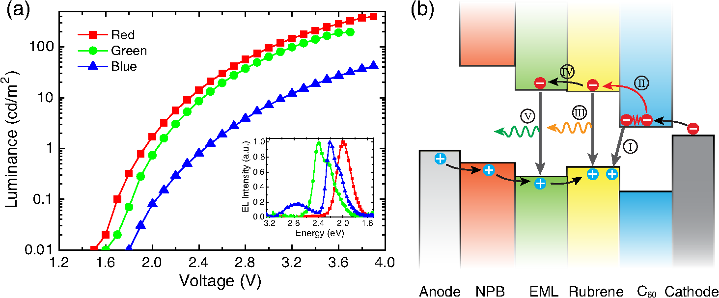 As schematically shown in Fig. 10(b), the electronic processes of I, II, and III are similar to that for Auger heterojunction devices shown in Fig. 8(b). The difference is the Auger-electrons in the LUMO of Rubrene, which are injected into EMLs [process IV in Fig. 10(b)], and these injected Auger-electrons recombine radiative with holes in EMLs to generate light emission [process V in Fig. 10(b)]. The Auger-electron injection thus enables EMLs at photon energies higher than the applied electrical energies. 4.3.Turn-on Voltages of Organic Light-Emitting Diodes with Auger-Electron InjectionAs a result of Auger-electron injection, the turn-on voltages of OLEDs are no longer limited by the HOMO–LUMO energy gaps of the emitter molecules. Figure 11(a) shows the turn-on voltages of devices versus the energy gaps of the emitter molecules. This figure clearly shows two regions, denoted by I and II, with a division line on which turn-on voltages equal to the energy gaps of the emitters. In standard OLEDs, the energy for charge injection into the emissive layer come from applied bias voltages and therefore typical OLEDs operate in region I. But it is clear that OLEDs with Auger-electron injection all fall into region II. According to the above discussion, a formula, i.e., , has derived to govern the turn-on voltage of devices with Auger-electron injection. So, Fig. 11(b) shows the turn-on voltages of devices with Auger-electron injection versus the energy differences between the HOMOs of HTLs and the LUMOs of ETLs. As shown in Fig. 11(b), the experimental data are in excellent agreement with the theoretical prediction. Fig. 11(a) Turn-on voltages of devices with Auger-electron injection versus the energy gaps of the emitters. (b) Turn-on voltages of devices with Auger-electron injection versus the energy difference between the HOMOs of HTLs and the LUMOs of ETLs.20 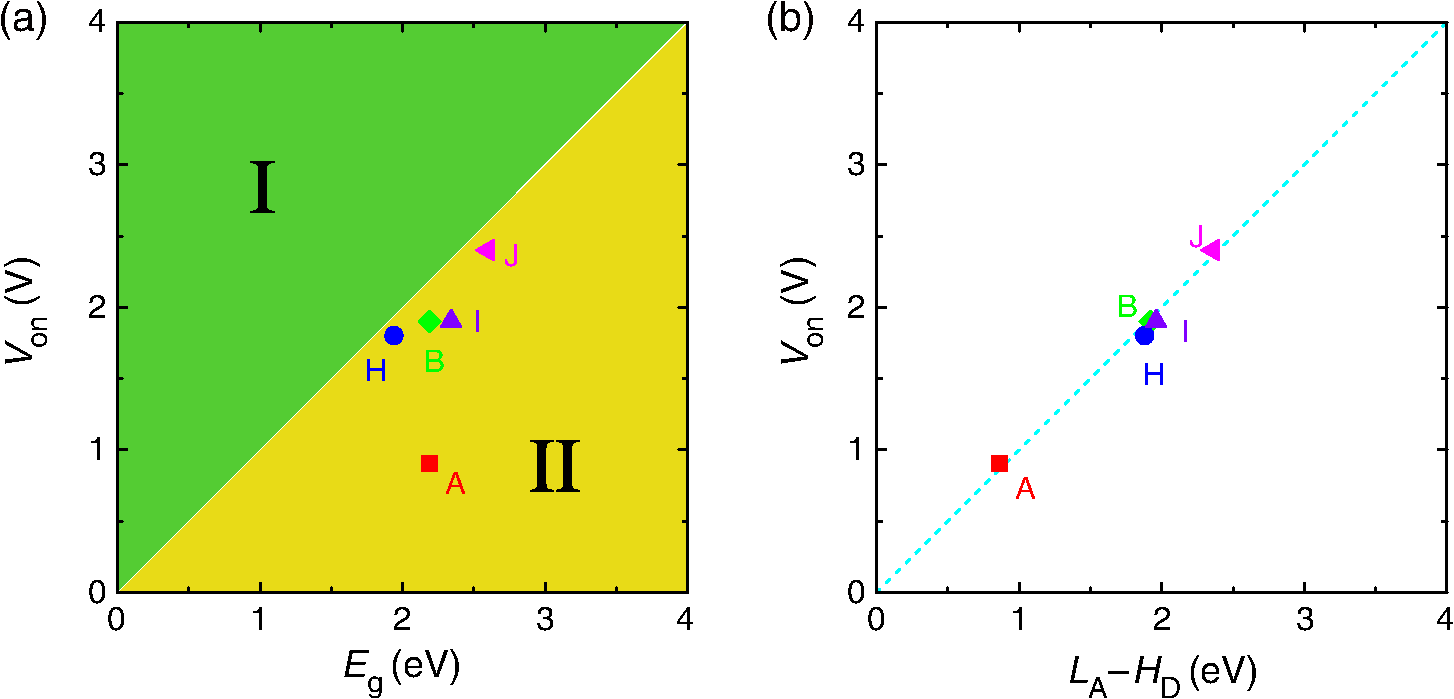 5.ConclusionThis paper presents a mini review on interface CT excitonic processes at organic heterojunctions and ultralow-voltage Auger-electron stimulated OLEDs. Auger-electron emission at organic heterojunctions has sufficient energy to overcome the energy barriers and thus Auger-electron can be injected into the LUMO of HTL. This Auger-electron injection acts a built-in voltage booster leading to working voltages far below the HOMO–LUMO energy gaps of the emitter molecules. The Auger-electron injection provides a new pathway to fabricate ultralow-voltage OLEDs. AcknowledgmentsWe would like to acknowledge the funding support from the National Natural Science Foundation of China (Grant No. U1402273), the Natural Science and Engineering Research Council of Canada, from Yunnan Province’s Department of Science and Technology (Grant No. 2013FA002), and the Research Excellence Fund of Yunnan University (Grant No. YNU201403). ReferencesM. A. Mccarthy et al.,
“Low-voltage, low-power, organic light-emitting transistors for active matrix displays,”
Science, 332
(6029), 570
–573
(2011). http://dx.doi.org/10.1126/science.1203052 SCIEAS 0036-8075 Google Scholar
J. Kido et al.,
“Multilayer white light-emitting organic electroluminescent device,”
Science, 267
(5202), 1332
–1334
(1995). http://dx.doi.org/10.1126/science.267.5202.1332 SCIEAS 0036-8075 Google Scholar
S. Reineke et al.,
“White organic light-emitting diodes with fluorescent tube efficiency,”
Nature, 459
(7244), 234
–238
(2009). http://dx.doi.org/10.1038/nature08003 Google Scholar
Y. L. Chang and Z. H. Lu,
“White organic light-emitting diodes for solid-state lighting,”
J. Display Technol., 9
(6), 459
–468
(2013). http://dx.doi.org/10.1109/JDT.2013.2248698 IJDTAL 1551-319X Google Scholar
M. A. Baldo et al.,
“Highly efficient phosphorescent emission from organic electroluminescent devices,”
Nature, 395
(6698), 151
–154
(1998). http://dx.doi.org/10.1038/25954 Google Scholar
M. A. Baldo et al.,
“Very high-efficiency green organic light-emitting devices based on electrophosphorescence,”
Appl. Phys. Lett., 75
(1), 4
(1999). http://dx.doi.org/10.1063/1.124258 APPLAB 0003-6951 Google Scholar
U. Hiroki et al.,
“Highly efficient organic light-emitting diodes from delayed fluorescence,”
Nature, 492
(7428), 234
–238
(2012). http://dx.doi.org/10.1038/nature11687 Google Scholar
Q. Zhang et al.,
“Efficient blue organic light-emitting diodes employing thermally activated delayed fluorescence,”
Nat. Photonics, 8
(4), 326
–332
(2014). http://dx.doi.org/10.1038/nphoton.2014.12 NPAHBY 1749-4885 Google Scholar
C. W. Tang et al.,
“Electroluminescence of doped organic thin films,”
J. Appl. Phys., 65
(9), 3610
–3616
(1989). http://dx.doi.org/10.1063/1.343409 JAPIAU 0021-8979 Google Scholar
L. C. Won and L. J. Yeob,
“Organic light-emitting diodes: above 30% external quantum efficiency in blue phosphorescent organic light-emitting diodes using pyrido[2, 3-b] indole derivatives as host materials,”
Adv. Mater., 25
(38), 5450
–5454
(2013). http://dx.doi.org/10.1002/adma.201301091 ADVMEW 0935-9648 Google Scholar
Y.-S. Park et al.,
“Exciplex-forming co-host for organic light-emitting diodes with ultimate efficiency,”
Adv. Funct. Mater., 23
(39), 4914
–4920
(2013). http://dx.doi.org/10.1002/adfm.v23.39 AFMDC6 1616-301X Google Scholar
J.-H. Lee et al.,
“An exciplex forming host for highly efficient blue organic light emitting diodes with low driving voltage,”
Adv. Funct. Mater., 25
(3), 361
–366
(2015). http://dx.doi.org/10.1002/adfm.201402707 AFMDC6 1616-301X Google Scholar
M. Pfeiffer et al.,
“Electrophosphorescent p–i–n organic light-emitting devices for very-high-efficiency flat-panel displays,”
Adv. Mater., 14
(22), 1633
–1636
(2002). http://dx.doi.org/10.1002/1521-4095(20021118)14:22<1633::AID-ADMA1633>3.0.CO;2-# ADVMEW 0935-9648 Google Scholar
M. G. Helander et al.,
“Chlorinated indium tin oxide electrodes with high work function for organic device compatibility,”
Science, 332
(6032), 944
–947
(2011). http://dx.doi.org/10.1126/science.1202992 SCIEAS 0036-8075 Google Scholar
J. Huang et al.,
“Low-voltage organic electroluminescent devices using pin structures,”
Appl. Phys. Lett., 80
(80), 139
–141
(2002). http://dx.doi.org/10.1063/1.1432110 APPLAB 0003-6951 Google Scholar
G. He et al.,
“High-efficiency and low-voltage p-i-n electrophosphorescent organic light-emitting diodes with double-emission layers,”
Appl. Phys. Lett., 85
(17), 3911
–3913
(2004). http://dx.doi.org/10.1063/1.1812378 APPLAB 0003-6951 Google Scholar
A. K. Pandey and J.-M. Nunzi,
“Upconversion injection in rubrene/perylene-diimide-heterostructure electroluminescent diodes,”
Appl. Phys. Lett., 90
(26), 263508
(2007). http://dx.doi.org/10.1063/1.2752540 APPLAB 0003-6951 Google Scholar
A. K. Pandey and J. M. Nunzi,
“Rubrene/fullerene heterostructures with a half-gap electroluminescence threshold and large photovoltage,”
Adv. Mater., 19
(21), 3613
–3617
(2007). http://dx.doi.org/10.1002/(ISSN)1521-4095 ADVMEW 0935-9648 Google Scholar
L. Qian et al.,
“Electroluminescence from light-emitting polymer/ZnO nanoparticle heterojunctions at sub-bandgap voltages,”
Nano Today, 5
(5), 384
–389
(2010). http://dx.doi.org/10.1016/j.nantod.2010.08.010 NTAOCG 1748-0132 Google Scholar
S.-J. He et al.,
“Auger-electron-stimulated organic electroluminescence at ultralow voltages below the energy gap,”
Phys. Rev. Appl., 3
(5), 054011
(2015). http://dx.doi.org/10.1103/PhysRevApplied.3.054011 PRAHB2 2331-7019 Google Scholar
S. J. He et al.,
“Tunable excitonic processes at organic heterojunctions,”
Adv. Mater., 28
(4), 649
–654
(2016). http://dx.doi.org/10.1002/adma.201504287 ADVMEW 0935-9648 Google Scholar
M. Pope and C. E. Swenberg, Electronic Processes in Organic Crystals and Polymers, Oxford University Press, New York
(1999). Google Scholar
M. Pope et al.,
“Charge-transfer exciton state and energy levels in tetracene crystal,”
J. Chem. Phys., 43
(9), 3367
–3371
(1965). http://dx.doi.org/10.1063/1.1726399 JCPSA6 0021-9606 Google Scholar
J. F. Wang et al.,
“Exciplex electroluminescence from organic bilayer devices composed of triphenyldiamine and quinoxaline derivatives,”
Adv. Mater., 10
(3), 230
–233
(1998). http://dx.doi.org/10.1002/(ISSN)1521-4095 ADVMEW 0935-9648 Google Scholar
M. Cocchi et al.,
“Efficient exciplex emitting organic electroluminescent devices,”
Appl. Phys. Lett., 80
(13), 2401
–2403
(2002). http://dx.doi.org/10.1063/1.1467614 APPLAB 0003-6951 Google Scholar
K. Goushi and C. Adachi,
“Efficient organic light-emitting diodes through up-conversion from triplet to singlet excited states of exciplexes,”
Appl. Phys. Lett., 101
(2), 023306
(2012). http://dx.doi.org/10.1063/1.4737006 APPLAB 0003-6951 Google Scholar
K. Goushi et al.,
“Organic light-emitting diodes employing efficient reverse intersystem crossing for triplet-to-singlet state conversion,”
Nat. Photonics, 6
(4), 253
–258
(2012). http://dx.doi.org/10.1038/nphoton.2012.31 NPAHBY 1749-4885 Google Scholar
X. K. Liu et al.,
“Prediction and design of efficient exciplex emitters for high-efficiency, thermally activated delayed-fluorescence organic light-emitting diodes,”
Adv. Mater., 27
(14), 2378
–2383
(2015). http://dx.doi.org/10.1002/adma.v27.14 ADVMEW 0935-9648 Google Scholar
D. Chen et al.,
“Fluorescent organic planar pn heterojunction light-emitting diodes with simplified structure, extremely low driving voltage, and high efficiency,”
Adv. Mater., 28
(2), 239
–244
(2016). http://dx.doi.org/10.1002/adma.v28.2 ADVMEW 0935-9648 Google Scholar
A. Weller, The Exciplex, 23
–38 Academic Press Inc., London
(1975). Google Scholar
Y. S. Park et al.,
“Energy transfer from exciplexes to dopants and its effect on efficiency of organic light-emitting diodes,”
J. Appl. Phys., 110
(12), 124519
(2011). http://dx.doi.org/10.1063/1.3672836 JAPIAU 0021-8979 Google Scholar
D.-Y. Zhou et al.,
“Host to guest energy transfer mechanism in phosphorescent and fluorescent organic light-emitting devices utilizing exciplex-forming hosts,”
J. Phys. Chem. C, 118
(41), 24006
–24012
(2014). http://dx.doi.org/10.1021/jp508228z JPCCCK 1932-7447 Google Scholar
T. Főrster,
“10th spiers memorial lecture. transfer mechanisms of electronic excitation,”
Discuss. Faraday Soc., 27 7
–17
(1959). http://dx.doi.org/10.1039/DF9592700007 DFSOAW 0014-7664 Google Scholar
D. L. Dexter,
“A theory of sensitized luminescence in solids,”
J. Chem. Phys., 21
(5), 836
–850
(1953). http://dx.doi.org/10.1063/1.1699044 JCPSA6 0021-9606 Google Scholar
H. Shin et al.,
“Blue phosphorescent organic light-emitting diodes using an exciplex forming co-host with the external quantum efficiency of theoretical limit,”
Adv. Mater., 26
(27), 4730
–4734
(2014). http://dx.doi.org/10.1002/adma.v26.27 ADVMEW 0935-9648 Google Scholar
K. H. Kim et al.,
“Highly efficient organic light-emitting diodes with phosphorescent emitters having high quantum yield and horizontal orientation of transition dipole moments,”
Adv. Mater., 26
(23), 3844
–3847
(2014). http://dx.doi.org/10.1002/adma.201305733 ADVMEW 0935-9648 Google Scholar
K. H. Kim et al.,
“Phosphorescent dye-based supramolecules for high-efficiency organic light-emitting diodes,”
Nat. Commun., 5 4769
(2014). http://dx.doi.org/10.1038/ncomms5769 NCAOBW 2041-1723 Google Scholar
X. K. Liu et al.,
“Nearly 100% triplet harvesting in conventional fluorescent dopant-based organic light-emitting devices through energy transfer from exciplex,”
Adv. Mater., 27
(12), 2025
–2030
(2015). http://dx.doi.org/10.1002/adma.v27.12 ADVMEW 0935-9648 Google Scholar
E. M. Kober et al.,
“Application of the energy gap law to excited-state decay of osmium (II)-polypyridine complexes: calculation of relative nonradiative decay rates from emission spectral profiles,”
J. Phys. Chem., 90
(16), 3722
–3734
(1986). http://dx.doi.org/10.1021/j100407a046 JPCHAX 0022-3654 Google Scholar
S. J. He et al.,
“A simple organic diode structure with strong rectifying characteristics,”
Org. Electron., 15
(11), 3370
–3374
(2014). http://dx.doi.org/10.1016/j.orgel.2014.09.018 OERLAU 1566-1199 Google Scholar
J. Iveland et al.,
“Direct measurement of Auger electrons emitted from a semiconductor light-emitting diode under electrical injection: identification of the dominant mechanism for efficiency droop,”
Phys. Rev. Lett., 110
(17), 177406
(2013). http://dx.doi.org/10.1103/PhysRevLett.110.177406 PRLTAO 0031-9007 Google Scholar
W. K. Bae et al.,
“Controlling the influence of Auger recombination on the performance of quantum-dot light-emitting diodes,”
Nat. Commun., 4 2661
(2013). http://dx.doi.org/10.1038/ncomms3661 NCAOBW 2041-1723 Google Scholar
S. A. Moskalenko and D. W. Snoke, Bose-Einstein Condensation of Excitons and Biexcitons: and Coherent Nonlinear Optics with Excitons, 140 Cambridge University Press, Cambridge, United Kingdom
(2000). Google Scholar
D. Bimberg, Semiconductor Nanostructures, 243
–245 Springer Science & Business Media, Springer, New York
(2008). Google Scholar
R. Matsunaga et al.,
“Observation of charged excitons in hole-doped carbon nanotubes using photoluminescence and absorption spectroscopy,”
Phys. Rev. Lett., 106
(3), 037404
(2011). http://dx.doi.org/10.1103/PhysRevLett.106.037404 PRLTAO 0031-9007 Google Scholar
A. K. Pandey,
“Highly efficient spin-conversion effect leading to energy up-converted electroluminescence in singlet fission photovoltaics,”
Sci. Rep., 5 7787
(2015). http://dx.doi.org/10.1038/srep07787 SRCEC3 2045-2322 Google Scholar
C. Xiang et al.,
“Origin of sub-bandgap electroluminescence in organic light-emitting diodes,”
Small, 11
(40), 5439
–5443
(2015). http://dx.doi.org/10.1002/smll.v11.40 SMALBC 1613-6810 Google Scholar
M. Ullah et al.,
“Singlet fission and triplet exciton dynamics in rubrene/fullerene heterojunctions: implications for electroluminescence,”
Adv. Electron. Mater., 1
(12), 1500229
(2015). http://dx.doi.org/10.1002/aelm.201500229 Google Scholar
Q. Chen et al.,
“Determining the origin of half-bandgap-voltage electroluminescence in bifunctional rubrene/C60 devices,”
Sci. Rep., 6 25331
(2016). http://dx.doi.org/10.1038/srep25331 SRCEC3 2045-2322 Google Scholar
BiographyShou-Jie He received his BSc degree in physics in 2010 from Yunnan University, China. He is currently a PhD student in the Department of Physics, Yunnan University, under the supervision of Zheng-Hong Lu. His research focuses on the electronic processes at organic heterojunctions. Zheng-Hong Lu received his BSc degree in physics from Yunnan University, China, in 1983, and his PhD in engineering physics from Ecole Polytechnique of Montreal, Canada, in 1989. Currently, he is a full professor and a Tier I Canada Research Chair in organic optoelectronics at the University of Toronto, and he also held a special-invited professorship at Yunnan University. His lab is working on developing materials and devices for OLED flat-panel display, solid-state lighting, and solar cells. He has published over 300 technical papers and contributed to several book chapters. |


