|
|
1.IntroductionSurface plasmon polaritons (SPPs) are plasma oscillations of free electrons coupled with optical fields localized along the interface of a metal and a dielectric.1,2 SPPs are promising for several applications including optical data center interconnects,3–6 solar cells,7–9 and bio(chemical) sensors.10–15 In such applications, surface plasmons (SPs) are excited by light and supported on a variety of metal and dielectric structures including planar arrangements of metal and dielectric films,16 metal gratings (or hole arrays),5,17,18 a prism,19 a metal edge,20,21 and metal nanoparticles such as islands, spheres, rods,22,23 or nanoantennas.24,25 The ability of SPs to resonate or propagate on metallic structures enables them to have interesting and useful attributes such as high bulk and surface sensitivities, subwavelength confinement and energy asymptotes in dispersion curves which have led to many different applications. Recently the decay of plasmons into hot carriers (electrons or holes) has attracted considerable interest26 due to applications in energy harvesting, photocatalysis, and photodetection.27 Specifically, an SP photodetector is a device capable of converting an optical signal to an electrical signal by detecting SPs (light) or involving them in the photodetection mechanism. Such photodetectors typically combine a metallic structure that supports SPPs with photonic detection based on internal photoemission (IPE) or electron-hole pair (EHP) creation. IPE is useful for detection of light at energies below the bandgap of the semiconductor when incident radiation of energy is greater than the Schottky barrier energy, , and is of particular interest to extend the detection bandwidth of technologically important materials such as Si.28 However, the creation of EHPs in the semiconductor is more efficient and dominates over IPE when is greater than the bandgap energy of the semiconductor . In terms of photodetection, hot (energetic) carrier devices are typically formed by placing the metal surface in contact with a semiconductor,3,29 forming a Schottky barrier. Hot carriers generated from the nonradiative decay of SPPs can transport to the metal–semiconductor interface and can be injected into the conduction band of the semiconductor, resulting in photocurrent.30 The main advantages of these photodetectors reside in their extremely high speed, in their simple fabrication process, and their small dimensions, comparable to those of highly integrated electronic circuits.23,25 The internal quantum efficiency of IPE photodetectors is low compared to that of photodetectors based on EHP, and this limits their application in power monitoring and in the telecommunications fields. The low quantum efficiency is a direct result of hot carrier transport limitations, initially through the metal in which they are generated (due to scattering), then across the Schottky barrier and into the semiconductor, where hot carriers which do not have enough energy to overcome the Schottky barrier are reflected and do not contribute to photoemission. An additional factor limiting the external quantum efficiency (responsivity) is the low absorption of incident light by metals, as they are highly reflective. In recent years, new approaches and structures have been proposed in order to overcome such limitations. The generation of hot carriers in plasmonic nanostructures is a very promising energy conversion mechanism, and it has found interesting applications in photovoltaic and photocatalytic devices. Clavero has reviewed the fundamentals of hot-electron generation, injection, and regeneration in plasmonic nanostructures allowing optimum utilization of the solar spectrum,26 highlighting interesting applications in photovoltaic and photocatalytic devices. This new energy-conversion method holds the promise of high conversion efficiencies, while keeping fabrication costs low. Progress on SP photodetectors has been rapid, and interest on the topic continues to increase, prompting a review of the most recent works in this area. Brongersma et al.31 and Berini32 highlight many opportunities for the generation and use of plasmon-induced hot carriers in nanostructures. Our objectives in this review are to describe the operating principles behind SP photodetectors based on IPE, summarize the most recent progress in this area, and highlight avenues that appear promising. 2.Operating Principles of Internal Photoemission-Based DevicesWe first begin with some theoretical background useful to clarify the working principles of IPE-based devices. An time-harmonic dependence is assumed throughout. The relative permittivity is denoted as and is written for a metal in terms of real and imaginary parts as . denotes a generic wavevector and its magnitude. is the wavenumber of plane waves in vacuum, where is the wavelength in vacuum, is the speed of light in vacuum, and is the angular frequency. 2.1.Single Interface Surface Plasmon PolaritonsFigure 1 shows that the simplest planar structure sustaining SPPs is that of a single, flat interface between a dielectric, nonabsorbing half space () with positive real dielectric constant and an adjacent conducting half space () described via a dielectric function . This structure is termed the single interface SPP waveguide. The metallic character requires that . For metals, this condition is fulfilled at frequencies below the bulk plasmon frequency .1 Fig. 1Single-interface SPP and waveguide. The relative permittivity of the metal is denoted and that of the dielectric . The distribution of the main TE field component () of the SPP is sketched in blue on the structure. (Adapted from Ref. 33). 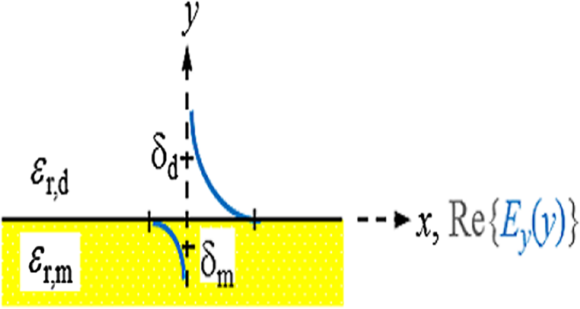 Highly conductive metals and good dielectrics are usually used to implement SPP structures. Au is a relevant and good choice given its chemical stability and low loss among the other metals. Ag and Cu are also good choices, but they are reactive so passivation is required. Other good choices are metals satisfying the condition ; nevertheless, many other materials may offer advantages for collecting these hot carriers. In Ref. 34, by considering the expected hot carrier distributions based on the electron density of states for 16 different materials ranging from metals (Au, Ag, Cu, Al, Fe, Pt, Ti, and Y), alloys (Ag-Cu, Al-Ga, Au-Pt, and AlOCu), and nanostructures (Ag and Au nanowires, carbon nanotubes, and graphene), the authors predicted the preferred hot carrier type for collection and their expected performance under different illumination conditions. Proper material selection is then achieved by knowing carrier energy distributions, which are extremely sensitive to the details of the electronic bandstructure. For example, Cu and Au generate hot holes that are much more energetic than electrons, while Ag and Al distribute energies more equitably between electrons and holes.35 Metals are dispersive at optical wavelengths. Away from intraband transitions, the permittivity can be accurately modeled via the Drude equation which captures their dispersive character1 where is the plasma frequency and is the relaxation time. The Drude region of the permittivity of a real metal corresponds to the region of the electromagnetic spectrum where Eq. (1) is approximately satisfied, which for several metals runs from the visible to the infrared. The permittivity approaches that of a perfect electric conductor as the wavelength increases into the far-infrared and beyond.The single-interface SPP waveguide supports a nonradiative SPP mode (one-bound) that is transverse magnetic (TM) and may propagate at any angle in the plane of the interface. The SPP fields (, and ) are confined in the direction, with maxima at the interface, and decaying into both media. The main transverse electric (TE) field component () of the SPP is sketched on the structure of Fig. 1 as the thick curve. The field penetration in the metal is much smaller than that in the dielectric . The SPP is confined because the metal and dielectric have of opposite signs at the wavelength of interest. The wavenumber of the single-interface SPP is given by:1 For a dielectric cladding that has no loss (), the above simplifies to the following approximate expressions for the real and imaginary parts of the wavenumber:1 Figure 2 gives the dispersion of the SPP ( in eV versus , is the Planck’s constant) on a single-interface33 with the light-line in plotted as the dash-dot curve. As the frequency decreases, the metal approaches a perfect electrical conductor, so the SPP confinement decreases and its dispersion merges with the light-line. As the frequency increases, the SPP dispersion approaches the energy asymptote, apparent in Fig. 2 near (), and becomes large.Fig. 2Dispersion curve of the SPP along a Ag/SiO2 semi-infinite interface; the light line in is plotted as the green dash-dot curve. (Adapted from Ref. 33). 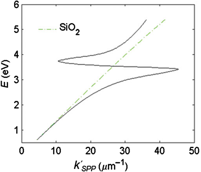 The optical density-of-states increases and the group velocity decreases near the energy asymptote. Bend-back in the SPP dispersion is observed for frequencies above the asymptote (), linking the bound SPP on the right of the light-line to the radiative SPP on the left. The bound SPP (right of the light line in Fig. 2) cannot be directly excited by incident light—an additional structure is needed in order to increase the in-plane wavenumber of the light to match that of the SPP; a corrugated grating or a prism is commonly used to accomplish this task.1 2.2.Internal PhotoemissionA conventional Schottky photodiode on n-type Si is sketched in Fig. 3(a),36 and used to describe two detection mechanisms that can be used to detect SPPs. The structure is convenient for the detection of SPPs because the latter may propagate along its metal surfaces, particularly along the metal–Si interface. Fig. 3(a) Schottky diode on n-Si illuminated by light of photon energy (green). Reverse biasing () is assumed. Electrons are shown by filled dark blue circles and holes by unfilled ones. (b) Energy band diagram of a Schottky contact on n-Si and the three-step IPE process consisting of , photoexcitation, , transport, , emission. and are the conduction and valence band edges, respectively, is the Fermi level, and is the Schottky barrier height. (Adapted from Ref. 32). 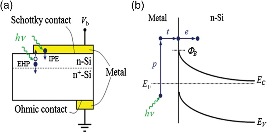 Two mechanisms for photodetection are sketched in Fig. 3(a): the first is the creation of EHPs in Si due to the absorption of incident radiation of energy greater than the bandgap energy . This mechanism, labeled EHP, involves the three steps of optical absorption and creation of EHPs, separation of EHPs, and transport under reverse bias for collection as the photocurrent. The second is the IPE of hot carriers (electrons in this case) created in the metal due to absorption of incident radiation of energy . This mechanism, labeled IPE, is described via the energy band diagram of Fig. 3(b); IPE is also a three-step process consisting of photoexcitation of hot (energetic) carriers in the metal, transport with scattering of hot carriers toward the metal–Si interface, and the emission of hot carriers over the Schottky barrier into the semiconductor where they are collected as the photocurrent. IPE requires that be greater than the Schottky barrier energy , and is a useful process for , i.e., for detection at energies below the semiconductor bandgap. The internal quantum efficiency is defined as the number of carriers that contribute to the photocurrent per absorbed photon per second where is the absorbed optical power and is the electronic charge.For detection using IPE, if and there is no bandgap then it can be assumed that the density of states is approximately constant, so is given approximately by37 for absorption in the metal only and near the Schottky contact. Example Schottky barriers are , 0.8, 0.58, and 0.72 eV for Au/p-Si, Au/n-Si, Al/p-Si, and Al/n-Si.36 At , ranges approximately from 0.3% to 9%. The external quantum efficiency and responsivity describe how a detector performs upon insertion in a system. is defined as where is the incident optical power. and are related by where is the absorptance, given byThe responsivity of a photodetector is given by the ratio of the photocurrent to the incident optical power and can be expressed in terms of and as IPE can be enhanced in several plasmonic structures as discussed in the following sections. It should be mentioned that the creation of EHPs can also be enhanced by involving SPPs. It is also important to mention that plasmon hot carrier generation results in higher-energy electrons than direct excitation.38 The probability for photon absorption is proportional to the square of the local electric field inside the metal. Planar metal surfaces reflect most of the incident light, and light absorption is not very efficient. The importance of plasmons to enhance light absorption in the near-surface region of a metal and consequently enhance photoemission processes was highlighted a long time ago.39 In metallic nanostructures, light absorption can be further enhanced by exciting localized SP resonances. This produces an antenna effect resulting in light collection from an area that is larger than the physical size of the nanostructure.40 The associated light concentration has been verified by, and used in, surface-enhanced processes, including Raman spectroscopy,41 photochemistry,42 and the photoexcitation of nearby quantum emitters.25 Knowledge of the imaginary part of the permittivity of a metal also provides a means for optimizing hot carrier generation. For instance, by tuning a plasmon mode to energies where the imaginary part of the permittivity is large, maximizing the hot carrier production is possible. This tuning can be performed either by exploiting the unique geometrical tunability of localized surface plasmon resonances (LSPRs) of metallic nanoparticles, or by fabricating composite structures consisting of both noble metals43 and metals with strong intraband transitions (such as transition metals).44 Figure 4(a) shows photoexcitation following the illumination of a metal nanoparticle with a femtosecond source pulse. Excitation of SPPs guides the flow of light (Poynting vector) toward and into the nanoparticle. Larger nanoparticles and shorter lifetimes result in higher carrier production rates but smaller energies.45 By following the trajectories of photoemitted electrons created by intense laser pulses, researchers have also been able to map the evanescent fields around plasmonic nanoparticles. In Fig. 4(b) one can see that electrons are preferentially emitted from regions of high field intensity (hot spots) and subsequently accelerated within the evanescent tail of plasmons resonating on nanoparticles. Fig. 4(a) Photoexcitation processes following the illumination of a metal nanoparticle with a femtosecond laser pulse; the excitation of a localized SP redirects the flow of light (Poynting vector) towards and into the nanoparticle. (Adapted from Refs. 31 and 46). (b) Simulation of field enhancement in a plasmonic bowtie nanoantenna and the resulting electron trajectories. (Adapted from Ref. 47).  This enables the steering of photoemitted carriers in directions determined by particle geometry.47 Precisely designed plasmonic nanostructures can significantly enhance photon absorption and convert incident light into hot carriers.48 3.Internal Photoemission-Based PhotodetectorsA Schottky barrier photodetector formed at the interface between a metal and a lightly doped semiconductor can be used to detect infrared radiation below the bandgap energy of the substrate via IPE.49,50 Such detectors involving SPP excitations in prism,51 grating-coupled detectors,52 waveguides3,53 and nanoparticles and nanoantennas10,29,54–56 have been reported; prism coupling to SPPs on a suitable detection structure was one of the first types of SPP detectors investigated in Ref. 57. The Otto coupling configuration used in these studies has been more popular in experimental work, mostly because the detection structures can be fabricated independently, then the prism can be aligned to the detector in the setup.32 3.1.Grating DetectorsA grating structure can be used as an alternative to a prism to increase the in-plane momentum of the incident light in order to match that of the SPP,1 providing compactness and manufacturing advantages and high detection sensitivity. In particular, the grating coupling method is convenient to excite SPPs on a detector,17,20 because the arbitrary wavenumber of the diffracted light can be generated by simply changing the grating pitch. The coupling condition of an SPP at a metal surface containing a grating is described by the following equation: where is the wavenumber of the SPP parallel to the metal surface, is the wavenumber of the incident light, is the angle of incidence of the light, is the grating order, and is the grating pitch. Gold nanogratings on Si have been shown to successfully couple incoming optical light to SPPs excited at the nanograting–Si interface.58 A metal-semiconductor (Schottky) nanograting structure has been proposed as an SPP photodetector,59,60 sensitive to the angle of incidence, polarization, and wavelength of light. The SPP photodetector consists of a Au/Si Schottky diode with a grating also used as the metal contact, and the detector converts SPP signals into photocurrent.61 Because the responsivity of the SPP detector is closely related to the SPP intensity at the Au/Si interface, the grating structure can be optimized in terms of the slit pitch and film thickness.4,62Figure 5 shows a grating structure forming an Au/Si Schottky-type SPP detector, producing a responsivity of (under no electrical bias).62 Fig. 5(a) Structure of Au/Si Schottky-type SPP detector with a nanoslit grating. (b) Slit pitch dependencies on SPP intensity and photocurrent for ring-type grating when slit pitch varies in the range of 440 to 1280 nm. (Adapted from Ref. 62). 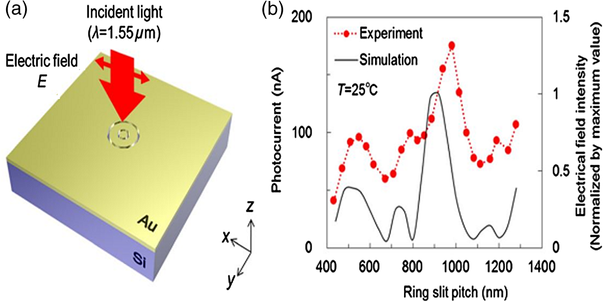 An efficient nanoslit grating arrangement that affects the phase conditions at both the air/Au interface and the Au/Si interface has been studied. When the slit pitch was nearly equal to an integral multiple of the SPP wavelength at the Au/Si interface, a higher intensity SPP mode was excited at the Au/Si interface outside the slits. Additionally, while the phase matching conditions were satisfied at the Au/Si interface, the antiphase interference of the SPP mode along the air/Au interface outside the slits was also confirmed. Experimentally, similar results were confirmed as an SPP photodetector with a ring-type grating that has a polarization-independent photocurrent. Light coupling, guiding, and photodetection can be combined in the same structure. Figure 6 shows a simple metal/semiconductor SPP structure consisting of an SPP waveguide and a detector where the SPP couples from the waveguide to the photodetector.4 The air/Au interface is used for guiding SPPs and the SPPs propagate at this interface without large losses. To convert the SPPs into an electrical signal using IPE, the propagating SPPs are coupled to the Au/Si interface by the diffraction structure consisting of a multislit structure and a disk array. A tunable laser was set to the wavelength of 1550 nm, emitting an optical power in the range of 0 to 10 mW. The photocurrents detected at the Au/Si interface are much larger when compared with those detected for the device without the diffraction structure (26 times for the multislit structure and 10 times for the disk array). This kind of device is targeted to be used as a low-loss SPP waveguide and detector in photonic integrated circuit applications and wavelength filters controlled by the slit pitches. Fig. 6Scanning electron micrographs (SEMs) of (a) a device used to evaluate the photoresponse measured by the devices with diffraction structures, (b) the multislit structure, (c) the disk array structure, and (d) no diffraction structure in place, (e) photoresponses of the devices with each of the diffraction structures, and (f) polarization angle dependence of the photocurrent detected by the device with the multislit structure. (Adapted from Ref. 4). 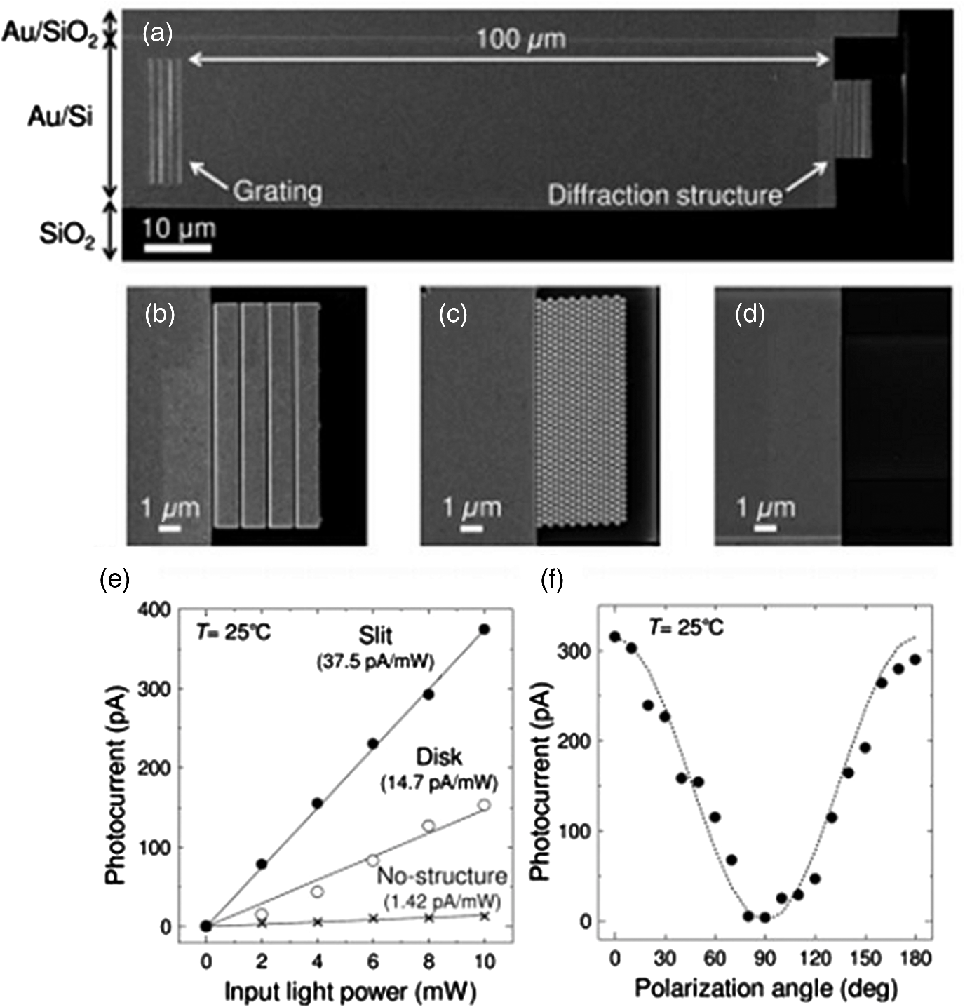 Sobhani et al. presented a grating Schottky photodetector based on IPE with the geometry shown in Fig. 7, enabling a three times narrower spectral response than observed for nanoantenna-based devices.27 The responsivity of this device ( at zero bias voltage) is similar to responsivities reported in the literature for SPP detectors.3 Fig. 7(a) Schematic of a gold grating on an n-type Si with a 2-nm Ti adhesion layer, oriented transverse to the laser polarization. The polarization of the incident beam and its vector are represented by yellow and green arrows, respectively, (b) SEM image of a gold grating structure with a grating thickness , interslit distance , and slit width . For all structures the array measured . The scale bar is . (c) Responsivities of grating-based photodetectors for three different gold layer thicknesses, (black), 170 nm (grey), and 200 nm (green), showing a strong intensity dependence on grating thickness. (Adapted from Ref. 27). 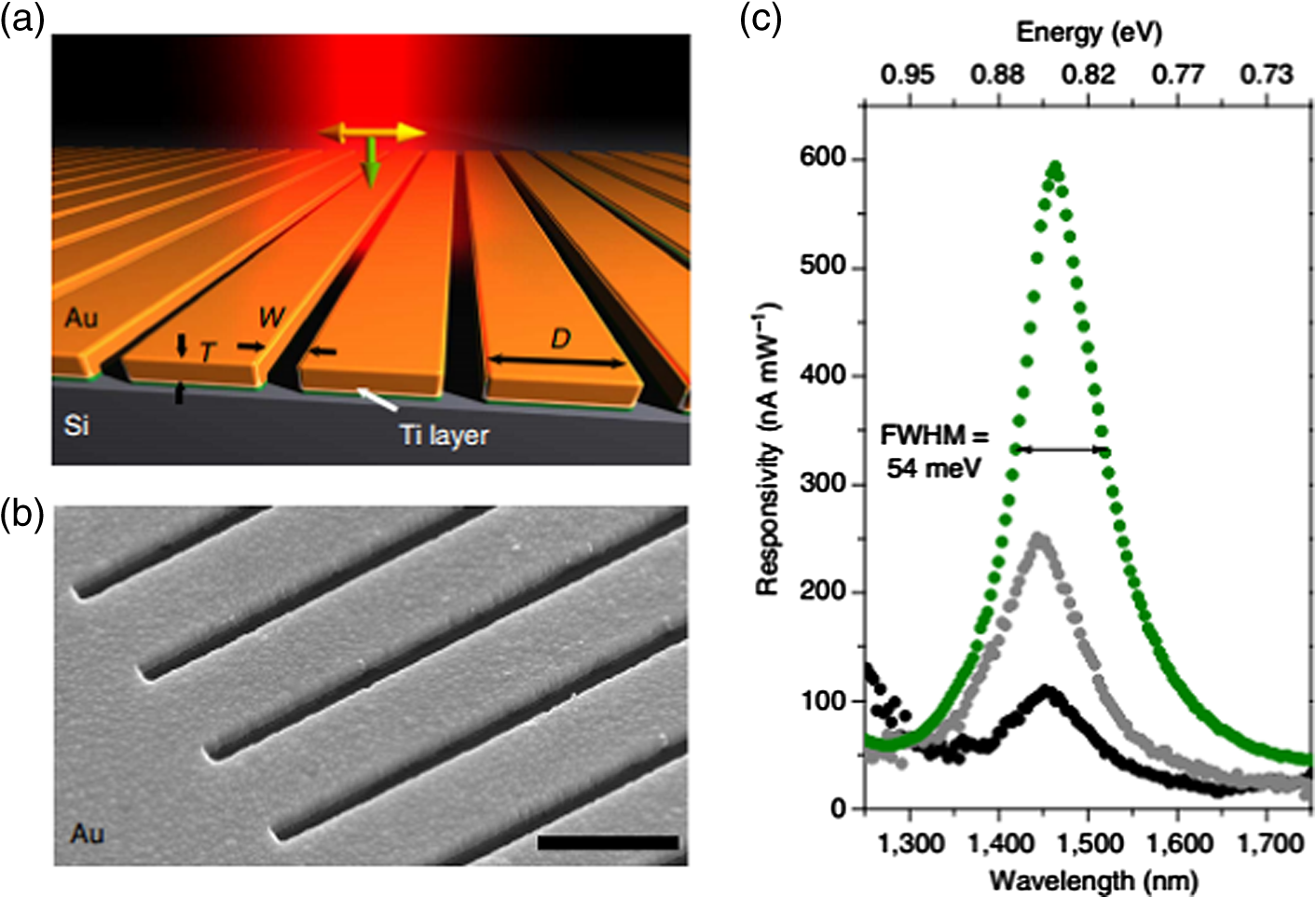 The internal quantum efficiency of this photodetector is , 20 times larger than the previously reported literature value of 0.01% for nanoantenna-based devices.29 Unlike previous devices, this responsivity maintains its narrow full width at half maximum (FWHM) bandwidth of nominally 54 meV, narrower by a factor of more than three compared to previously reported devices.29 Although studies have been carried out on various aspects of nanogratings and their detection applications, achieving a high infrared (subbandgap) responsivity over a broad spectral range on low-cost Si remains a difficult (and worthwhile) challenge. In Ref. 63, Alavirad et al. proposed a plasmonic Schottky photodetector consisting of a Au nanograting on a thin metal patch on -type Si, as shown in Fig. 8, providing detection via the IPE of hot holes generated in the patch along the Schottky contact. This structure produced some of the highest responsivities reported to date in the literature, of about (with no electrical bias) at . The RC time constant limited electrical bandwidth of this device is predicted to be up to . Gathered into arrays, these small area devices are capable of aggregating bandwidths into the range. These detectors have many important advantages such as simplicity, compatibility with silicon, and low-cost fabrication. Fig. 8(a) SEMs of an uncoated nanograting photodetector. The pitch of the device is measured as 406 nm (400 nm designed) and the thickness of the Au patch is measured as 29.8 nm (20 nm designed) and its duty cycle of this is 60%. (b) Measured photocurrent response of three grating photodetectors; , , and 410 nm, duty cycle of 62% and patch diameter of . (c) Photocurrent generated by grating detectors versus incident power measured for three different pitches. A linear fit is applied to the data and the slope corresponds to the responsivity of the device. (Adapted from Ref. 63).  3.2.MIM, MOM, MSM, and MIS DetectorsOther nanostructures investigated as SPP photodetectors include gratings or arrays of metal nanowires on metal–oxide–semiconductor structures (MOS),64 metal–oxide–metal (MOM) structures,65 or on a commercial photodiode.66 In these planar junctions, the excitation of propagating SPPs can enhance efficiency. Brongersma et al. have examined the phenomenon of photocurrent generation by hot electrons in wavelength-scale metal–insulator–metal (MIM) tunneling devices67 and enhanced their efficiency by reshaping one of the metal contacts of the junction into an array of metal nanowires that support resonating SPPs, as depicted in Fig. 9. The voltage dependence, spectral dependence, nanowire width dependence, and polarization dependence of the photocurrent were examined experimentally. Fig. 9(a) Schematic illustration of a typical device featuring a series of MIM crossbar junctions formed between a wide bottom electrode and a set of nanoscale top electrodes. The directions of the electric field for TE and TM illumination are as depicted. (b) SEM image of a device with a 470-nm-wide top electrode. The inset shows a cross-sectional image of the device, composed of an oxide layer sandwiched by top and bottom metal layers. (c) Photocurrent image of the device taken at an illumination wavelength of 400 nm with TM polarization overlaid on the SEM image of the device. The red color corresponds to 7 pA and blue indicates a close to zero photocurrent. (Adapted from Ref. 67). 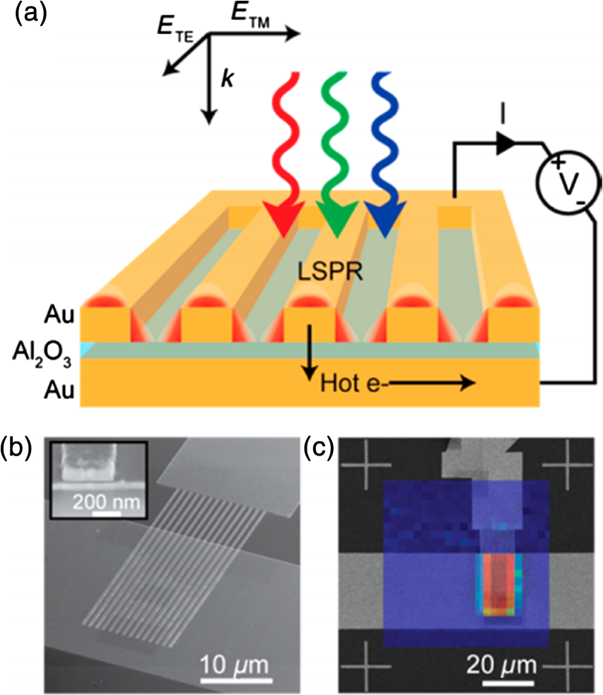 Figure 9(c) shows an image photocurrent taken from a device with a 470-nm-wide stripe overlaid on its SEM image (no bias voltage). It is clearly observed that photocurrent is generated only in the regions where the top electrodes overlay the wide bottom electrode to form a series of nanoscale MIM junctions. Finally, they measured the spectral dependence of the responsivity of a detector with 750-nm-wide stripes upon illumination with TM polarized light with the bias voltages in the range from to and obtained a maximum value of in the visible range. In modern optical communication systems, high efficiency (realized from some parameters such as size, responsivity, dark current, and photocurrent) photodetectors at the communication window with the wavelength of 1550 nm are strongly desired. Wu et al. designed an MIM IPE-based photodetector exhibiting an unbiased responsivity of and an ultranarrow response band (), which promises to be a candidate as the compact photodetector operating in communication band.68 Casalino et al. presented a Si on insulator (SOI) waveguide metal–semiconductor–metal (MSM) photodetector, based on IPE and working at a wavelength of 1550 nm.69 Taking advantage of the MSM structure, their device is able to increase responsivity by lowering the barrier. At the same time, a very low dark current is achieved both by depositing a very small active metal area and by realizing a device with asymmetric electrodes.70 Figure 10(a) shows the SOI structure obtained by depositing the absorbing Cu metal strictly around the output vertical facet of an SOI rib waveguide. Fig. 10(a) Schematic of the proposed photodetector integrated with SOI waveguide and (b) responsivity versus reverse voltage applied at 1550 nm. (Adapted from Ref. 69). 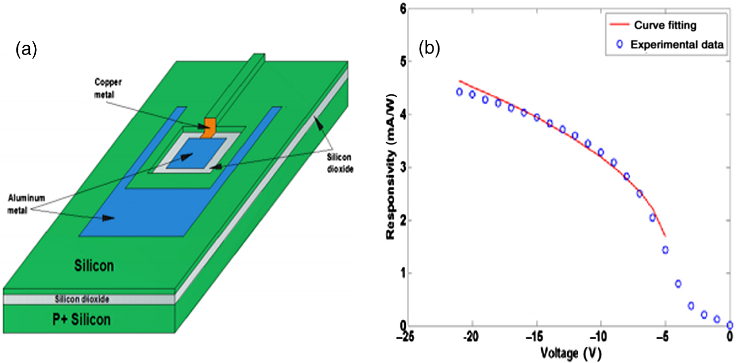 This active metal is in contact with a large Al pad deposited on the buried oxide layer of the SOI structure, and therefore, does not contribute to the dark current or the junction capacitance. A second large Al electrode was deposited on the Si substrate to collect the generated photocurrent. In Fig. 10(b), the responsivity of MSM photodetector versus bias voltage measured at 1550 nm is shown. It reaches a maximum value of about at . Another alternative for conventional metal–semiconductor Schottky junction is a choice of metal–insulator–semiconductor (MIS) heterojunction which significantly reduces dark current, resulting in increased device performance.71 3.3.Nanoparticles DetectorsIn recent years, plasmonic energy conversion has been proposed as a promising alternative to conventional electron–hole separation in semiconductor structures. This emerging method is based on the generation of hot carriers in plasmonic devices through the decay of SPs. LSPRs occur in well-designed nanostructures in which confined free electrons oscillate with the same frequency as the incident light and eventually enter resonance, giving rise to enhanced, highly localized electromagnetic fields. Therefore, such nanostructures have been investigated as very efficient light-trapping elements that can be integrated into photovoltaic cells to considerably increase the quantum efficiency of conventional schemes.26 Many studies have considered plasmonic hot-electron generation with applications to both photovoltaic and catalytic devices. Many of these studies considered Au or Ag nanoparticles in contact with ,72–75 as shown in Fig. 11. The Au-nanoislands (Au-NIs), annealed at 800°C, tightly contacted the surface and appeared to be incorporated into the interfacial structure atomic layers. Electron energy loss spectroscopy (EELS) measurements were obtained to characterize the interfacial structure of the . In EELS, the corresponding core edge [the titanium (Ti) edge] in the spectrum provides information about the electronic nanostructure and symmetry coordination of the excited atom. Measurements show extinction spectra of prepared under 800°C annealing. Although the extinction values at the peak wavelength are different, all the show plasmon peak at the wavelength range from 600 to 630 nm. Fig. 11(a) High-resolution transmission electron microscopy images of the cross-section at the interface of the Au-NIs and the annealed at 800°C. (b) The incident photocurrent efficiency action spectrum measured with the photoelectrode (red) and the extinction spectrum of the photoelectrode (black). The applied potential was 0.3 V versus a saturated calomel electrode. (Adapted from Ref. 73). 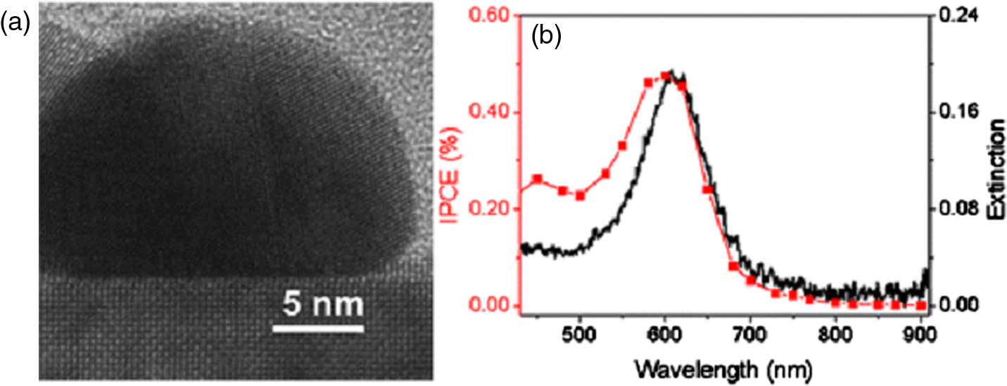 In further recent developments, multiple combinations of materials have been proposed to enable hot carrier detectors and catalytic devices. Some examples include multilayer assemblies of Pt nanoparticles on thin films,76 Ag-decorated nanotube arrays77 as shown in Fig. 12, ZnO nanorods decorated with Au nanoparticles,78 and hierarchical Au-ZnO flower-rod heterostructures79 as shown in Fig. 13. Referring to Fig. 12, Au nanoparticles are well dispersed on the surface of nanotubes of a metallic state. The SPP resonance (SPR) effect of Ag nanoparticles extends the visible light response and consequently enhances the absorption capacity of . They can also efficiently restrain the recombination of photo-generated EHPs in nanotubes. Experimental results prove that nanotube devices have better photocatalytic performance than pure nanotubes and their corresponding hydrogen evolution rate is 3.3 times as that of the latter. The Au/ZnO samples in Fig. 13 are made through a thermal decomposition method. Au nanoparticles were loaded on oriented hierarchical ZnO flower-rod heterostructures. Measurements reveal that there is an electronic interaction between the Au nanoparticles and ZnO flower-rods, and more oxygen molecules are adsorbed on the surface of Au/ZnO heterostructures. They show a strong absorbance in the visible region due to SPR and enhance the separation of EHPs, resulting in the improvement of photocatalytic activity under visible light radiation. Small metal nanoparticles exhibit resonant responses under optical excitation, dependent on the structure’s shape, size, and composition, the dielectric environment in which they find themselves, and the wavelength of illumination.23 Nazirzadeh et al. presented a broadband near-infrared (NIR) Si Schottky photodetector consisting of Au nanoislands (randomly sized) formed on an n-type Si substrate, fabricated by rapid thermal annealing of a thin Au film.56 Their device structure is shown in Fig. 14. Its potential monolithic integration with electronics makes it promising for ultralow-cost NIR imaging in large volume applications such as automotive and security, in addition to telecommunications. The measured photoresponse of the devices extend up to and the responsivities at 1.3 and are 2 and , respectively. Fig. 14(a) Depiction of broad-band NIR Si Schottky photodetector. Au nanoislands are formed on n-type Si by rapid thermal annealing of a thin Au film. Si substrate is used as the bottom contact and Au nanoislands together with the AZO capping layer constitute the top contact, (b) SEM image of the samples annealed at 450°C. (Adapted from Ref. 56). 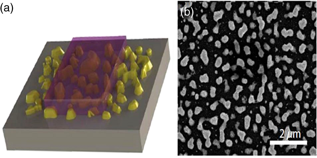 Several works have provided insight into the localization of hot electron generation in plasmonic nanostructures. Dombi et al. demonstrated the ultrafast generation of hot electrons from tailored metallic nanoparticles and realized the role of plasmonic field enhancement in this process by comparing resonant and off-resonant particles, as well as different nanorod geometries. These nanoparticles offer the possibility of tailoring nanoscale electric fields with high-level control over the plasmonic resonance, which can be overlapped with the spectrum of the exciting laser pulse to achieve field enhancements of the incident radiation by factors of up to several hundred.47 Kazuma et al.80 showed that sites in Ag nanorods on exposed to higher electromagnetic fields generate more hot electrons. After SPP excitation and hot electron generation, oxidized diffuse into the water layer, adsorb on the substrate, and eventually recombine with electrons from , leading to the formation of satellite redeposited Ag islands, as shown in Fig. 15 (top). Fig. 15Oxidation of Ag nanorods and redeposition of small Ag nanoparticles takes place as a result of plasmon-induced charge separation. After LSPR excitation and hot-electron generation, the oxidized diffuse in the water layer adsorbed on the substrate and eventually recombine with electrons from , forming satellite redeposited islands. The AFM images show Ag nanorods with various ARs that have undergone excitation of multipole plasmon modes from to 4 after irradiation with 800 nm. The rods experience changes in length depending on the incident wavelength and mode excited. The horizontal scale bars are 50 nm in length. (Adapted from Ref. 80). 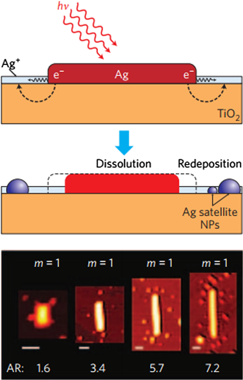 This effect was observed in nanorods with different aspect ratios (ARs) that sustained different multipole plasmon modes ( is 1, 2, 3, 4), as shown in the atomic force microscopy (AFM) images in the bottom of Fig. 15. Islands appeared in the regions where the SPP electromagnetic field was more intense, confirming the hypothesis that the charge generation process is induced and/or enhanced by the intense fields on the nanostructures. 3.4.Waveguide DetectorsSchottky photodetectors based on IPE, integrated with a thin metal stripe waveguide in symmetric81 and asymmetric50 claddings have also been proposed, operating with long range and single-interface SPPs, respectively. Figure 16(a) shows a sketch of an asymmetric SPP waveguide photodetector consisting of a thin narrow metal stripe on Si with air on top.50 Structures were fabricated as Au or Al stripes on n-Si forming Schottky contacts thereon.50 The mode,82 localized to the metal–Si interface, was excited at wavelengths below the bandgap of Si via butt-coupling to a tapered polarization-maintaining single mode fiber (PM-SMF). This mode propagates along the metal–Si interface with strong absorption, creating hot carriers in the metal along the Schottky contact, some of which cross over the Schottky barrier and are collected as the photocurrent. Figure 16(b) presents the spectral response in Fowler form of a Au stripe of width and thickness 135 nm on n-Si, for a reverse bias of 0.2 V and an incident optical power of 2 mW.50 The intercept with the abscissa yields the cut-off photon energy, , corresponding to a cut-off wavelength of . Responsivities up to 1 mA/W were reported with this photodetector schematic. Figure 16(c) shows a measured photocurrent map of a Au on p-Si detector, generated by scanning a tapered PM-SMF over the end facet [following Fig. 16(a)] using a piezoelectric nanopositioner.6 The Au stripe width and thickness in this case were and 40 nm, the reverse bias was 0.1 V, the incident optical power was 1 mW, and the excitation wavelength was 1310 nm. The photocurrent was largest when the PM-SMF was perfectly aligned with the stripe maximizing the overlap between the incident beam and the mode of the waveguide. Fig. 16(a) Sketch of an SPP waveguide detector consisting of a metal stripe forming a Schottky contact on Si, excited in the mode82 via butt-coupling to a tapered polarization-maintaining single mode fiber (PM-SMF). (Adapted from Ref. 50). (b) Spectral response of a Au on n-Si detector as sketched in (a), plotted in Fowler form. The Au stripe width and thickness were and 135 nm, the reverse bias was 200 mV and the incident optical power was 2 mW. (Adapted from Ref. 50). (c) Photocurrent map () of a Au on p-Si detector as sketched in (a), generated by scanning a tapered PM-SMF over the end facet using a piezoelectric nanopositioner. The Au stripe width and thickness were and 40 nm (sketched as the black horizontal line), the reverse bias was 100 mV, the incident optical power was 1 mW, and the excitation wavelength was 1310 nm. (Adapted from Ref. 6). 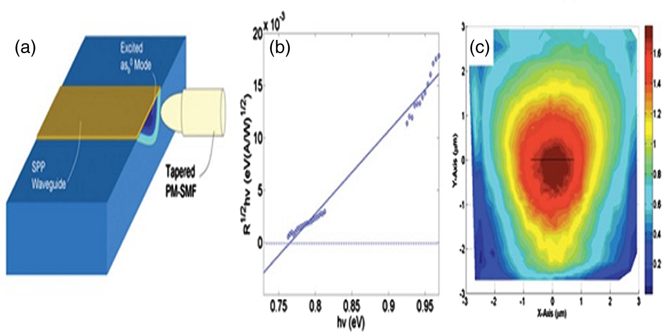 Other studies involving asymmetric metal stripe Schottky detectors include operation under a strong reverse bias approaching breakdown where a increase in responsivity relative to low bias was reported,83 and a performance comparison of such detectors for two metals on p-Si and n-Si, two SPP modes of operation, and several stripe geometries.84 3.5.Optical Antenna DetectorsThe electric near-fields produced by nanoantennas can be of much greater intensity than the incident electric fields,10 therefore, the photodetection volume can shrink, potentially leading to faster devices with compelling signal to noise characteristics.85 Mousavi et al. investigated an SPP photodetector concept based on the enhancement of electrical near-field in low-defect, low-doped detection volumes located in the gaps of an array of metal nanodipole antennas.24 Significant enhancement in responsivity in the presence of nanodipoles at telecom wavelengths is predicted ( at 1550 nm). The 3-dB electrical bandwidth of the device is estimated based on its RC rise time and the hole transit time through the detection volume for the cases of conventional and ballistic transport in InGaAs and is found to range from to 4 THz. Knight et al. reported an active optical monopole array which can be considered as a highly compact, wavelength-specific, and polarization-specific light detector.29 Desiatov et al. proposed a nanoscale broadband Si plasmonic Schottky photodetector with high responsivity and improved signal-to-noise ratio operating in the subbandgap regime.55 Figures 17(a) and 17(b) show SEM images of a typical fabricated device.55 The apex of pyramid was found to be . Due to the large cross-section of the pyramid, light is collected from a large area which corresponds to its base, concentrated toward the nanoapex of the pyramid, absorbed in the metal, and generates hot electrons. At the apex of the pyramid, the electric field intensity is enhanced by a factor of compared with the electromagnetic intensity in the base of the silicon pyramid. Theoretical investigation proves that most of the hot electrons are generated in the metallic part of the pyramid close to the pyramid’s apex. Figure 16(c) shows the measured characteristic of a typical device for different wavelengths of illumination at a constant incident optical power. The responsivity of the device is found to be 5, 12, and for incident optical wavelengths of 1550, 1300, and 1064 nm, respectively. Fig. 17SEM images of a plasmonic enhanced Si pyramids, (a) formation of the nanoapex in the silicon pyramid. (b) SEM image of a final fabricated device, (c) measurements of the pyramid Schottky device at constant optical power for three different wavelengths and dark measurement. The inset shows the photocurrent versus optical power data and linear fit for 1550 nm wavelength. (Adapted from Ref. 55). 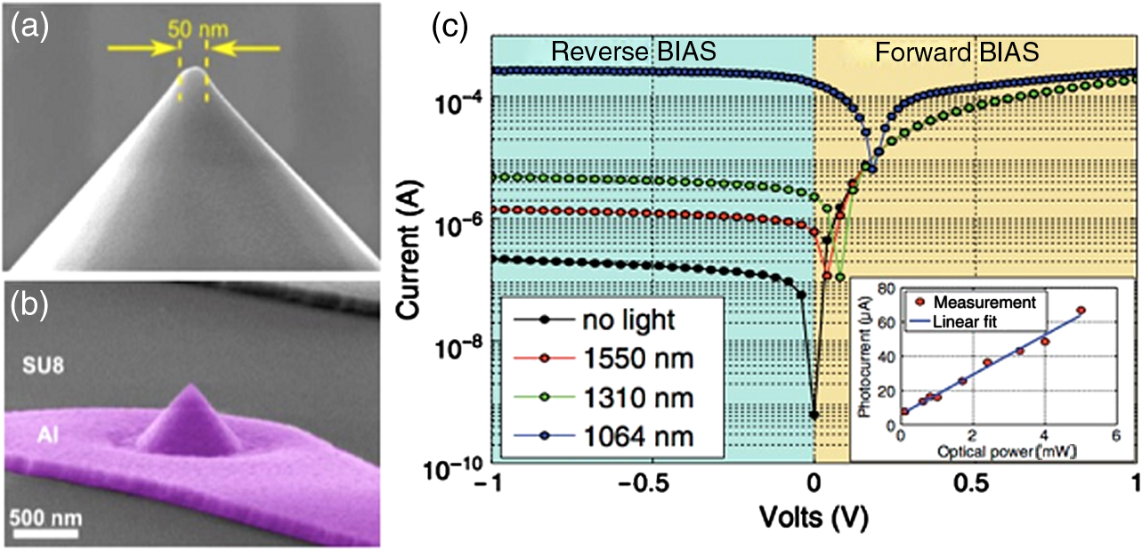 In addition to the ability in tunability of the operating wavelength and bandwidth in SPP photodetectors, there are many interesting plasmonic structures which enable a straightforward tailoring of the polarization dependence. In the past decade, SPRs have been employed in creating metamaterials offering interesting optical properties such as strong chirality86 which is some orders of magnitude higher than that of chiral molecules. Distinguishing between the two polarizations of circularly polarized light (CPL) is an inherent issue and a big problem with conventional photodetectors due to the fact that conventional semiconductors lack intrinsic chirality. Li et al. proposed a nanoantenna CPL photodetector in which the ability to distinguish left-handed circularly polarized (LCP) light and right-handed circularly polarized (RCP) light are obtained from the engineered chirality in metamaterial plasmonic nanostructures.87 Figure 18(a) shows a periodic array of chiral metamaterials consisting of a unit cell of a Ag nanoantenna on top of a PMMA spacer and an optically thick layer of Ag as the backplane forming a Schottky interface between Si and Ag nanowires. Generated hot electrons can then be captured and the high circular dichroism directly leads to enhanced discrimination between LCP and RCP in the CPL photodetectors. Figures 18(b) and 18(c) show two fabricated (left-hand) LH and (right-hand) RH chiral metamaterials arrays and their theoretical and experimental responses. Responsivities are obtained by illuminating the metamaterials with a CP laser source and measuring photocurrent as a function of the laser handedness and wavelength. The peak value for responsivity is corresponding to a quantum efficiency of which is two times that of chiral organic semiconductor transistors reported in Ref. 88. Fig. 18(a) Schematic of the CPL detector consisting of a chiral metamaterial integrated with a semiconductor that serves as a hot electron acceptor. The Ohmic contact on Si is formed by soldering indium. The circuit is formed by wire bonding to the silver bus bar and indium, (b, c) photoresponsivity spectra of experimentally measured (dots) and theoretically calculated (solid curve) under LCP (blue) and RCP (red) illumination for (b) LH and (c) RH metamaterials. (Adapted from Ref. 87). 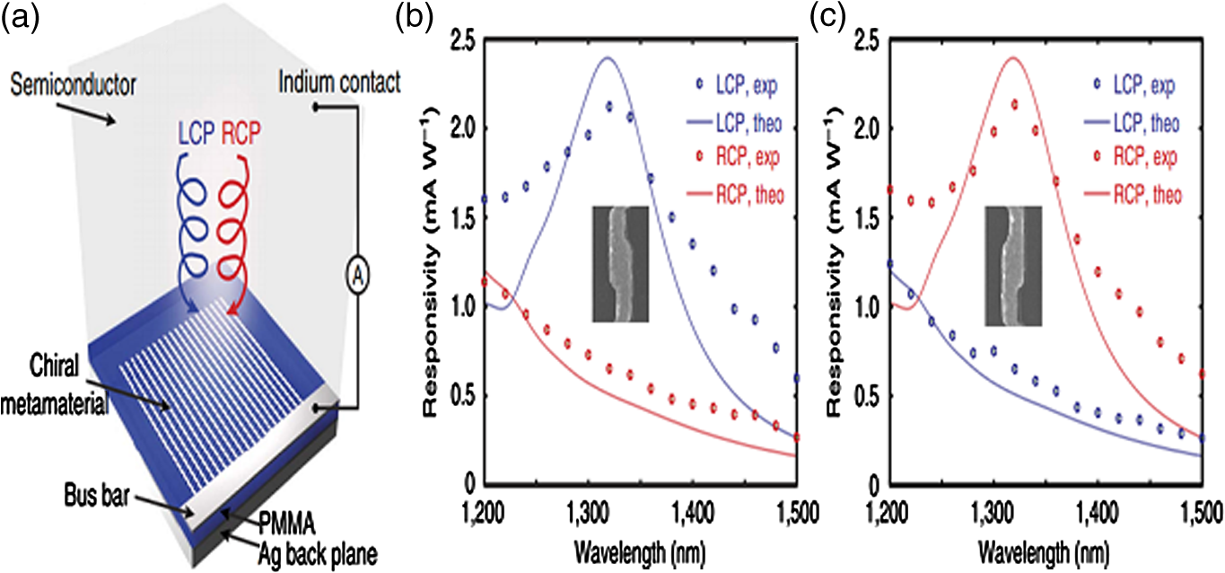 One can combine this CPL photodetector with existing linearly polarized IPE photodetectors and make a hot electron polarimeter with the ability to determine the Stokes parameters or the states of polarization of an arbitrarily polarized beam 3.6.Theoretical Investigations and ProposalsA complete review of the theory of IPE in Schottky junctions has been reported, and the Vickers model enriched by Casalino et al.89 The conventional Fowler equation used in the description of IPE was modified. They propose an analytical formulation to calculate the metal thickness that maximizes the efficiency of the devices. An important point addressed by this work is to determine if IPE-based Si devices have the potential to compare with photodetectors based on III-V compounds (e.g., GaAs and GaAsIn) and play a key role in telecommunications. In general, plasmonic nanostructures are deposited on top of the semiconductor, which is convenient from the fabrication point of view, but this causes only a small percentage of hot electrons to be excited with a wavevector permitting transport across the Schottky barrier. Embedding the nanostructure into the semiconductor introduces vertical Schottky interfaces, which permit emission of ballistic electrons over the Schottky barriers into the semiconductor, increasing the internal quantum efficiency. Scales and Berini presented phenomenological models for the internal quantum efficiency of Schottky barrier photodetectors suitable for the detection of optical radiation below the bandgap energy of the semiconductor based on IPE from the metal into the semiconductor substrate.37 They studied both single and two Schottky barrier configurations. The double-barrier case provides higher enhancement due to emission over two barriers. The models proposed are based on assessing the emission probability of hot carriers as a function of their energy, taking into account multiple reflections within the metal film and energy losses due to internal scattering. Following this model, a Schottky contact detector comprising a symmetric metal stripe buried in p-type Si, capable of detecting SPPs at wavelengths below the bandgap of Si, is described in Ref. 81. End-fire coupled responsivities of about and minimum detectable powers of about are predicted at room temperature. They also comprehensively studied the internal quantum efficiency, responsivity, and sensitivity of symmetric surface-plasmon waveguide Schottky detectors, consisting of a thin metal stripe buried in Si. Responsivities of 0.1 to and receiver sensitivities of and are predicted for 1.5 and 10 GHz electrical bandwidths ( and ), respectively. Knight et al. determined that embedded nanowires under normal incidence can produce a greater efficiency than comparable planar Schottky devices.90 This clearly suggests that three-dimensional (3-D) Schottky barriers can be a key design feature for increasing the efficiency of plasmon-based photodetection. A polarization-insensitive and high-efficiency plasmonic subbandgap Si Schottky photodetector operating at telecom wavelengths via IPE is proposed in Ref. 91. The proposed structure, shown in Fig. 19(a), consists of a Si ridge waveguide, a Au Schottky electrode (of thickness ) covering both the top and sidewalls of the Si ridge, an aluminum (Al) Ohmic electrode on top of the Si slab, and a thin SU8 insulating film (of thickness ) separating the two electrodes. The hot carrier emission probability is a very important factor in the estimation of the internal quantum efficiency. Depending on the configuration of the structure, the emission cone may consist of one of the subfigures shown in Fig. 19(b). For the proposed detector, for Au-Si round interfaces follows the same expression as that for flat interfaces [See Fig. 19(b) top-right side one]. By comparison with a diode with only a top Au contact, the polarization-dependent responsivity is significantly minimized in this photodetector and higher responsivities for both TE and TM polarizations are achieved over a very broad wavelength range of 1.2 to . Fig. 19(a) 3-D schematic diagram of the proposed Si photodetector, (b) emission cones with angle, : (top-left) a momentum-space illustration; (top-right) real-space illustrations for round Au-Si interfaces, and (bottoms) an asymmetric corner denoted by the red dashed rectangles when (left) and (right) , (c) responsivity, , for both TE (solid lines) and TM (dotted lines) polarizations, and (d) PDD of responsivity, for photodetectors with , 30, 50, 70, and 90 nm. The SU8 film thickness is . (Adapted from Ref. 91). 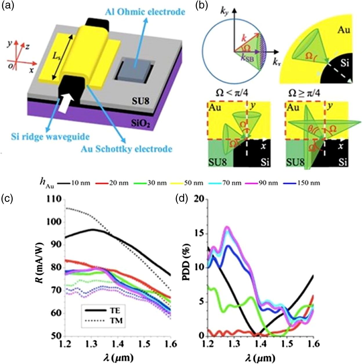 Figures 19(c) and 19(d) show the effects of on the responsivity () and polarization-dependent deviation (PDD) of the device. Specifically, changing changes the total absorption and the responsivity of the detector and also the polarization dependence of the responsivity. When , the absorption spectrum no longer changes very much for both TE and TM polarizations, because the optical field is tightly confined to the Au-Si interfaces and it can be sufficiently absorbed with a 50-nm-thick Au film. However, PDD is very large over the whole wavelength range for . As decreases, PDD decreases first and then quickly increases. At , the internal quantum efficiency is the highest in each part of the Au film among all the cases. Therefore, the responsivity spectrum rises to the highest level, especially in the short wavelength range, even though the absorption spectrum lies in the same range as the other cases with larger . In this case, the internal quantum efficiency dominates the responsivity spectrum. 4.SummaryThis review highlights opportunities for the generation and use of plasmon-induced hot carriers in metallic nanostructures on semiconductors. EHP creation and IPE have both been used extensively as detection mechanisms. Interest in IPE is motivated by the fact that it enables subbandgap detection so the optical bandwidth of a detector can be extended to photon energies below the bandgap of the semiconductor. IPE-based SPP photodetectors typically combine a metallic structure that supports SPPs, such as a planar or grating structure, metallic nanoparticles, or holes in metal films, with a semiconductor detector structure such as a Schottky or pn junction. Several investigations aim at improving the efficiency of detectors based on IPE by exciting SPPs along a metal contact forming the device. Target applications of IPE are very broad, but improving the efficiency of solar cells and providing infrared detection at telecom wavelengths in Si are frequently evoked. Although performance and reliability of SPP-induced hot carrier generation has been comprehensively proposed and observed in many works highlighted in this review paper, further fundamental studies are needed to optimize these processes for viable technological applications. Particularly, it will be important to determine more precisely the timescales involved in hot carrier relaxation and what physical and chemical parameters influence these timescales. Properties inherent to SPPs are exploited to convey useful characteristics to detectors in addressing applications such as low-noise high-speed detection, single-plasmon detection, near- and midinfrared imaging, solar energy conversion, and (bio)chemical sensing. The prospects for combining SPPs with detection structures are bright. Finally, it is worth summarizing some of described photodetector architectures involving SPPs and LSPRs that appear particularly promising as follows. 4.1.GratingsEarly investigations were based on grating-coupled detector structures. Corrugated grating couplers were used initially to create integrated and compact structures which are of high interest today. Table 1 briefly reviews the structures and characteristics of the devices explained in this paper. Table 1Characteristics of some grating-based photodetectors.
Note: Other interesting similar structures can be found in Refs. 2, 17, and 58–61. 4.2.MIM, MOM, MSM, and MISReferring to the point that in modern optical communication systems, size, responsivity, dark current, and photocurrent of a detector are very important, these kinds of detector structures are popular for high-speed operation because the contact architecture lowers the capacitance and carrier transit times. It is promising to design the contacts in such a detector simultaneously as a nanowire grating to couple incident light to SPPs thereon, such that they overlap strongly with the detection region. Table 2 briefly reviews the structures and characteristics of the devices explained in this paper. Table 2Characteristics of some MIM and MSM photodetectors.
Note: Other interesting similar structures can be found in Refs. 64–66 and 71. 4.3.NanoparticlesAs light strikes metal nanoparticles, SPP resonances can be excited thereon, high near-field enhancement factors can be generated, and strong absorption or scattering leading to light trapping can occur. These effects are useful to increase the absorptance of detectors, particularly those based on a thin absorption layer, or at wavelengths where the absorption is low. These effects are promising to improve the performance of thin-film Si or organic solar cells with application to photovoltaic and catalytic devices. Table 3 briefly reviews the structures and characteristics of the devices explained in this paper. Table 3Characteristics of some nanoparticles-based photodetectors.
Note: Other interesting similar structures can be found in Refs. 72, 74–76, and 78. 4.4.WaveguidesSPP waveguides can be formed into SPP photodetectors by replacing a dielectric region with a detection medium. Such detectors are attractive because they can be integrated with other plasmonic or photonic waveguides, they can increase the absorptance, shrink dimensions, enhance the detection process by exploiting enhanced or localized guided fields, and provide broad electrical and optical bandwidths. Table 4 briefly reviews the structures and characteristics of the devices explained in this paper. Table 4Characteristics of some waveguide-based photodetectors.
Note: Other interesting similar structures can be found in Refs. 50 and 81–83. 4.5.NanoantennasOptical nanoantennas are passive structures that capture part of an incident optical wave to produce oscillating near-fields at defined locations along its geometry. Combining this function with photodetection leads to integrated nanoscale photodetectors having compelling characteristics, as the antennas allow the detection volume to shrink, leading to fast devices with high signal-to-noise characteristics, and to polarization-resolved spectroscopic nanodetectors. Such properties have attracted much interest lately, due to the implications they have both in fundamental research and in technological applications. Table 5 briefly reviews the structures and characteristics of the devices explained in this paper. Table 5Characteristics of some nanoantennas-based photodetectors.
Note: Other interesting similar structures can be found in Refs. 10 and 85–86. ReferencesS. A. Maier, Plasmonics: Fundamentals and Applications, Springer Science+Business Media, New York
(2007). Google Scholar
D. K. Gramotnev and S. I. Bozhevolnyi,
“Nanofocusing of electromagnetic radiation,”
Nat. Photonics, 4 83
–91
(2010). http://dx.doi.org/10.1038/nphoton.2009.282 NPAHBY 1749-4885 Google Scholar
A. Akbari, R. N. Tait and P. Berini,
“Surface plasmon waveguide Schottky detector,”
Opt. Exp., 18 8505
–8514
(2010). http://dx.doi.org/10.1364/OE.18.008505 OPEXFF 1094-4087 Google Scholar
M. Fukuhara et al.,
“Low-loss waveguiding and detecting structure for surface plasmon polaritons,”
Appl. Phys. Lett., 104 081111
(2014). http://dx.doi.org/10.1063/1.4866792 APPLAB 0003-6951 Google Scholar
A. Olivieri et al.,
“Plasmonic nanostructured metal–oxide–semiconductor reflection modulators,”
Nano Lett., 15
(4), 2304
–2311
(2015). http://dx.doi.org/10.1021/nl504389f NALEFD 1530-6984 Google Scholar
P. Berini, A. Olivieri and C. Chen,
“Thin Au surface plasmon waveguide Schottky detectors on p-Si,”
Nanotechnology, 23 444011
(2012). http://dx.doi.org/10.1088/0957-4484/23/44/444011 NNOTER 0957-4484 Google Scholar
H. A. Atwater and A. Polman,
“Plasmonics for improved photovoltaic devices,”
Nat. Mater., 9 205
–213
(2010). http://dx.doi.org/10.1038/nmat2629 NMAACR 1476-1122 Google Scholar
S. W. Baek et al.,
“Plasmonic forward scattering effect in organic solar cells: a powerful optical engineering method,”
Sci. Rep., 3 1726
(2013). http://dx.doi.org/10.1038/srep01726 SRCEC3 2045-2322 Google Scholar
A. J. Leenheer et al.,
“Solar energy conversion via hot electron internal photoemission in metallic nanostructures: efficiency estimates,”
J. Appl. Phys., 115 134301
(2014). http://dx.doi.org/10.1063/1.4870040 Google Scholar
M. Alavirad et al.,
“Schottky-contact plasmonic dipole rectenna concept for biosensing,”
Opt. Express, 21
(4), 4328
–4347
(2013). http://dx.doi.org/10.1364/OE.21.004328 OPEXFF 1094-4087 Google Scholar
A. E. Cetin et al.,
“Handheld high-throughput plasmonic biosensor using computational on-chip imaging,”
Light Sci. Appl., 3 e122
(2014). http://dx.doi.org/10.1038/lsa.2014.3 Google Scholar
M. Alavirad, L. Roy and P. Berini,
“Optimization of plasmonic nanodipole antenna arrays for sensing applications,”
IEEE J. Sel. Top. Quant., 20
(3), 7
–14
(2014). http://dx.doi.org/10.1109/JSTQE.2013.2289963 IJSQEN 1077-260X Google Scholar
W. R. Wong et al.,
“Detection of dengue NS1 antigen using long-range surface plasmon waveguides,”
Biosens. Bioelectron., 78 132
–139
(2016). http://dx.doi.org/10.1016/j.bios.2015.11.030 BBIOE4 0956-5663 Google Scholar
W. R. Wong, F. R. M. Adikan and P. Berini,
“Long-range surface plasmon Y-junctions for referenced biosensing,”
Opt. Express, 23
(24), 31098
–31108
(2015). http://dx.doi.org/10.1364/OE.23.031098 OPEXFF 1094-4087 Google Scholar
P. Béland, O. Krupin and P. Berini,
“Selective detection of bacteria in urine with a long-range surface plasmon waveguide biosensor,”
Biomed. Opt. Express, 6
(8), 2908
–2922
(2015). http://dx.doi.org/10.1364/BOE.6.002908 BOEICL 2156-7085 Google Scholar
P. Berini,
“Long-range surface plasmon polaritons,”
Adv. Opt. Photonics, 1 484
–588
(2009). http://dx.doi.org/10.1364/AOP.1.000484 ASADD4 0733-4230 Google Scholar
T. Aihara et al.,
“Monolithic integration of surface plasmon detector and metal-oxide–semiconductor field-effect transistors,”
IEEE Photon. J., 5 6800609
(2013). http://dx.doi.org/10.1109/JPHOT.2013.2272779 Google Scholar
M. Toma et al.,
“Surface plasmon-coupled emission on plasmonic Bragg gratings,”
Opt. Express, 20 14042
(2012). http://dx.doi.org/10.1364/OE.20.014042 OPEXFF 1094-4087 Google Scholar
Z. Liu et al.,
“Enhanced backward scattering by surface plasmon on silver film,”
Appl. Phys. A, 87 157
–160
(2007). http://dx.doi.org/10.1007/s00339-006-3833-4 Google Scholar
H. Hu et al.,
“Efficient end-fire coupling of surface plasmons on flat metal surfaces for improved plasmonic Mach-Zehnder interferometer,”
J. Appl. Phys., 113 053101
(2013). http://dx.doi.org/10.1063/1.4789809 JAPIAU 0021-8979 Google Scholar
T. Aihara and M. Fukuda,
“Transmission properties of surface-plasmon-polariton coherence,”
Appl. Phys. Lett., 100 213115
(2012). http://dx.doi.org/10.1063/1.4723715 APPLAB 0003-6951 Google Scholar
K. L. Kelly et al.,
“The optical properties of metal nanoparticles: the influence of size, shape, and dielectric environment,”
J. Phys. Chem. B, 107 668
–677
(2003). http://dx.doi.org/10.1021/jp026731y JPCHAX 0022-3654 Google Scholar
M. Pelton, J. Aizpurua and G. Bryant,
“Metal-nanoparticle plasmonics,”
Laser Photonics Rev., 2 136
–159
(2008). http://dx.doi.org/10.1002/lpor.v2:3 LPRAB8 1863-8880 Google Scholar
S. S. Mousavi, A. Stöhr and P. Berini,
“Plasmonic photodetector with terahertz electrical bandwidth,”
Appl. Phys. Lett., 104
(14), 143112
(2014). http://dx.doi.org/10.1063/1.4870974 APPLAB 0003-6951 Google Scholar
P. Bharadwaj, B. Deutsch and L. Novotny,
“Optical antennas,”
Adv. Opt. Phot., 1 438
–483
(2009). http://dx.doi.org/10.1364/AOP.1.000438 AOPAC7 1943-8206 Google Scholar
C. Clavero,
“Plasmon-induced hot-electron generation at nanoparticle/metaloxide interfaces for photovoltaic and photocatalytic devices,”
Nat. Photon., 8 95
–103
(2014). http://dx.doi.org/10.1038/nphoton.2013.238 NPAHBY 1749-4885 Google Scholar
A. Sobhani et al.,
“Narrowband photodetection in the near-infrared with a plasmon-induced hot electron device,”
Nat. Commun., 4 1643
(2013). http://dx.doi.org/10.1038/ncomms2642 NCAOBW 2041-1723 Google Scholar
M. Casalino et al.,
“Near-infrared sub-bandgap all-silicon photodetectors: state of the art and perspectives,”
Sensors, 10 10571
–10600
(2010). http://dx.doi.org/10.3390/s101210571 SNSRES 0746-9462 Google Scholar
M. W. Knight et al.,
“Photodetection with active optical antennas,”
Science, 332 702
–704
(2011). http://dx.doi.org/10.1126/science.1203056 SCIEAS 0036-8075 Google Scholar
A. M. Brown et al.,
“Nonradiative plasmon decay and hot carrier dynamics: effects of phonons, surfaces, and geometry,”
ACS Nano, 10
(1), 957
–966
(2016). http://dx.doi.org/10.1021/acsnano.5b06199 ANCAC3 1936-0851 Google Scholar
M. L. Brongersma, N. J. Halas and P. Nordlander,
“Plasmon-induced hot carrier science and technology,”
Nat. Nanotechnol., 10 25
–34
(2015). http://dx.doi.org/10.1038/nnano.2014.311 NNAABX 1748-3387 Google Scholar
P. Berini,
“Surface plasmon photodetectors and their applications,”
Laser Photonics Rev., 8
(2), 197
–220
(2014). http://dx.doi.org/10.1002/lpor.201300019 LPRAB8 1863-8880 Google Scholar
P. Berini,
“Figures of merit for surface plasmon waveguides,”
Opt. Express, 14 13030
–13042
(2006). http://dx.doi.org/10.1364/OE.14.013030 OPEXFF 1094-4087 Google Scholar
T. Gong and J. N. Munday,
“Materials for hot carrier plasmonics,”
Opt. Mater. Express, 5
(11), 2501
–2512
(2015). http://dx.doi.org/10.1364/OME.5.002501 Google Scholar
R. Sundararaman et al.,
“Theoretical predictions for hot-carrier generation from surface plasmon decay,”
Nat. Commun., 5 5788
(2014). http://dx.doi.org/10.1038/ncomms6788 NCAOBW 2041-1723 Google Scholar
S. M. Sze, Physics of Semiconductor Devices, Wiley, New York
(1981). Google Scholar
C. Scales and P. Berini,
“Thin-film Schottky barrier photodetector models,”
IEEE J. Quant. Electr., 46 633
–643
(2010). http://dx.doi.org/10.1109/JQE.2010.2046720 Google Scholar
B. Y. Zheng et al.,
“Distinguishing between plasmon-induced and photoexcited carriers in a device geometry,”
Nat. Commun., 6 7797
(2015). http://dx.doi.org/10.1038/ncomms8797 NCAOBW 2041-1723 Google Scholar
J. E. Sipe and J. Becher,
“Surface-plasmon-assisted photoemission,”
J. Opt. Soc. Am., 71 1286
–1288
(1981). http://dx.doi.org/10.1364/JOSA.71.001286 JOSAAH 0030-3941 Google Scholar
S. Oldenburg et al.,
“Nanoengineering of optical resonances,”
Chem. Phys. Lett., 288 243
–247
(1998). http://dx.doi.org/10.1016/S0009-2614(98)00277-2 CHPLBC 0009-2614 Google Scholar
M. Moskovits,
“Surface enhanced spectroscopy,”
Rev. Mod. Phys., 57 783
–826
(1985). http://dx.doi.org/10.1103/RevModPhys.57.783 RMPHAT 0034-6861 Google Scholar
J. I. Gersten and A. Nitzan,
“Photophysics and photochemistry near surfaces and small particles,”
Surf. Sci., 158 165
–189
(1985). http://dx.doi.org/10.1016/0039-6028(85)90293-6 SUSCAS 0039-6028 Google Scholar
M. Bernardi et al.,
“Theory and computation of hot carriers generated by surface plasmon polaritons in noble metals,”
Nat. Commun., 6 7044
(2015). http://dx.doi.org/10.1038/ncomms8044 NCAOBW 2041-1723 Google Scholar
X. Li, D. Xiao and Z. Zhang,
“Landau damping of quantum plasmons in metal nanostructures,”
New J. Phys., 15 023011
(2013). http://dx.doi.org/10.1088/1367-2630/15/2/023011 NJOPFM 1367-2630 Google Scholar
A. Manjavacas et al.,
“Plasmon-induced hot carriers in metallic nanoparticles,”
ACS Nano, 8
(8), 7630
–7638
(2014). http://dx.doi.org/10.1021/nn502445f ANCAC3 1936-0851 Google Scholar
C. F. Bohren,
“How can a particle absorb more than the light incident on it?,”
Am. J. Phys., 51 323
–327
(1983). http://dx.doi.org/10.1119/1.13262 AJPIAS 0002-9505 Google Scholar
P. Dombi et al.,
“Ultrafast strong-field photoemission from plasmonic nanoparticles,”
Nano Lett., 13 674
–678
(2013). http://dx.doi.org/10.1021/nl304365e NALEFD 1530-6984 Google Scholar
H. Zhang and A. O. Govorov,
“Optical generation of hot plasmonic carriers in metal nanocrystals: the effects of shape and field enhancement,”
J. Phys. Chem. C, 118 7606
–7614
(2014). http://dx.doi.org/10.1021/jp500009k JPCCCK 1932-7447 Google Scholar
M. Casalino et al.,
“Critically coupled silicon fabry-perot photodetectors based on the internal photoemission effect at 1550 nm,”
Opt. Exp., 20 12599
–12609
(2012). http://dx.doi.org/10.1364/OE.20.012599 OPEXFF 1094-4087 Google Scholar
A. Akbari and P. Berini,
“Schottky contact surface-plasmon detector integrated with an asymmetric metal stripe waveguide,”
Appl. Phys. Lett., 95 021104
(2009). http://dx.doi.org/10.1063/1.3171937 APPLAB 0003-6951 Google Scholar
C. Daboo et al.,
“Improved surface plasmon enhanced photodetection at an AuGaAs Schottky junction using a novel molecular beam epitaxy grown onto coupling structure,”
Thin Solid Films, 201 9
–27
(1991). http://dx.doi.org/10.1016/0040-6090(91)90150-V THSFAP 0040-6090 Google Scholar
M. Tsuneyasu et al.,
“Sensitive detection of interleukin-6 on a plasmonic chip by grating-coupled surface-plasmon-field-enhanced fluorescence imaging,”
Jpn. J. Appl. Phys., 53 06JL05
(2014). http://dx.doi.org/10.7567/JJAP.53.06JL05 Google Scholar
I. Goykhman et al.,
“Waveguide based compact silicon Schottky photodetector with enhanced responsivity in the telecom spectral band,”
Opt. Express, 20
(27), 28594
–28602
(2012). http://dx.doi.org/10.1364/OE.20.028594 OPEXFF 1094-4087 Google Scholar
C.-Y. Tsai et al.,
“High sensitivity plasmonic index sensor using slablike gold nanoring arrays,”
Appl. Phys. Lett., 98 153108
(2011). http://dx.doi.org/10.1063/1.3C79536 APPLAB 0003-6951 Google Scholar
B. Desiatov et al.,
“Plasmonic enhanced silicon pyramids for internal photoemission Schottky detectors in the near-infrared regime,”
Opt. Lett., 2
(4), 335
–338
(2015). http://dx.doi.org/10.1364/OPTICA.2.000335 Google Scholar
M. A. Nazirzadeh et al.,
“Random sized plasmonic nanoantennas on Silicon for low-cost broad-band near-infrared photodetection,”
Sci. Rep., 4 7103
(2014). http://dx.doi.org/10.1038/srep07103 SRCEC3 2045-2322 Google Scholar
A. Sellai and P. Dawson,
“Quantum efficiency in GaAs Schottky photodetectors with enhancement due to surface plasmon excitations,”
Solid-State Electron., 46 29
–33
(2002). http://dx.doi.org/10.1016/S0038-1101(01)00283-0 Google Scholar
S. Hassan et al.,
“Fabrication of a plasmonic modulator incorporating an overlaid grating coupler,”
Nanotechnology, 25 495202
(2014). http://dx.doi.org/10.1088/0957-4484/25/49/495202 NNOTER 0957-4484 Google Scholar
J. W. Yoon et al.,
“Surface-plasmon mediated total absorption of light into silicon,”
Opt. Express, 19 20673
–20680
(2011). http://dx.doi.org/10.1364/OE.19.020673 OPEXFF 1094-4087 Google Scholar
X. G. Guo et al.,
“Surface plasmon-enhanced absorption in metal grating coupled terahertz quantum well photodetectors,”
IEEE J. Quantum Electron., 48 1113
–1119
(2012). http://dx.doi.org/10.1109/JQE.2012.2202637 Google Scholar
A. Takeda et al.,
“Sensitivity improvement of Schottky-type plasmonic detector,”
Proc. SPIE, 8923 89234G
(2013). http://dx.doi.org/10.1117/12.2033619 PSISDG 0277-786X Google Scholar
A. Takeda et al.,
“Schottky-type surface plasmon detector with nano-slit grating using enhanced resonant optical transmission,”
J. Appl. Phys., 116 084313
(2014). http://dx.doi.org/10.1063/1.4894150 JAPIAU 0021-8979 Google Scholar
M. Alavirad et al.,
“High-responsivity sub-bandgap hot-hole plasmonic Schottky detectors,”
Opt. Express, 24
(20), 22544
–22554
(2016). http://dx.doi.org/10.1364/OE.24.022544 OPEXFF 1094-4087 Google Scholar
H. Satoh and H. Inokawa,
“Surface plasmon antenna with gold line and space grating for enhanced visible light detection by a silicon-on-insulator metal-oxide–semiconductor photodiode,”
IEEE Trans. Nanotechnol., 11 346
–351
(2012). http://dx.doi.org/10.1109/TNANO.2011.2171194 ITNECU 1536-125X Google Scholar
J. A. Bean et al.,
“Performance optimization of antenna-coupled Au/AlOx/Pt tunnel diode infrared detectors,”
IEEE J. Quantum Electron., 47 126
–135
(2011). http://dx.doi.org/10.1109/JQE.2010.2081971 IEJQA7 0018-9197 Google Scholar
P. Genevet et al.,
“Holographic detection of the orbital angular momentum of light with plasmonic photodiodes,”
Nat. Commun., 3 1278
(2012). http://dx.doi.org/10.1038/ncomms2293 NCAOBW 2041-1723 Google Scholar
H. Chalabi, D. Schoen and M. L. Brongersma,
“Hot-electron photodetection with a plasmonic nanostripe antenna,”
Nano Lett., 14
(3), 1374
–1380
(2014). http://dx.doi.org/10.1021/nl4044373 NALEFD 1530-6984 Google Scholar
K. Wu et al.,
“Surface-plasmon enhanced photodetection at communication band based on hot electrons,”
J. Appl. Phys., 118 063101
(2015). http://dx.doi.org/10.1063/1.4928133 JAPIAU 0021-8979 Google Scholar
M. Casalino et al.,
“Asymmetric MSM sub-bandgap all-silicon photodetector with low dark current,”
Opt. Express, 21
(23), 28072
(2013). http://dx.doi.org/10.1364/OE.21.028072 OPEXFF 1094-4087 Google Scholar
C. Ng et al.,
“Hot carrier extraction with plasmonic broadband absorbers,”
ACS Nano, 10
(4), 4704
–4711
(2016). http://dx.doi.org/10.1021/acsnano.6b01108 ANCAC3 1936-0851 Google Scholar
F. P. G. de Arquer and G. Konstantatos,
“Metal-insulator-semiconductor heterostructures for plasmonic hot-carrier optoelectronics,”
Opt. Express, 23
(11), 14715
–14723
(2015). http://dx.doi.org/10.1364/OE.23.014715 OPEXFF 1094-4087 Google Scholar
A. Tanaka et al.,
“Gold-titanium(IV) oxide plasmonic photocatalysts prepared by a colloid-photodeposition method: correlation between physical properties and photocatalytic activities,”
Langmuir, 28 13105
–13111
(2012). http://dx.doi.org/10.1021/la301944b LANGD5 0743-7463 Google Scholar
X. Shi et al.,
“Plasmon-enhanced photocurrent generation and water oxidation with a gold nanoislandloaded titanium dioxide photoelectrode,”
J. Phys. Chem. C, 117 2494
–2499
(2013). http://dx.doi.org/10.1021/jp3064036 JPCCCK 1932-7447 Google Scholar
D. Gong et al.,
“Silver decorated titanate/titania nanostructures for efficient solar driven photocatalysis,”
J. Solid State Chem., 189 117
–122
(2012). http://dx.doi.org/10.1016/j.jssc.2011.11.036 JSSCBI 0022-4596 Google Scholar
Y. Fang et al.,
“Plasmon enhanced internal photoemission in antenna-spacer-mirror based nanostructures,”
Nano Lett., 15
(6), 4059
–4065
(2015). http://dx.doi.org/10.1021/acs.nanolett.5b01070 NALEFD 1530-6984 Google Scholar
Y. Shiraishi et al.,
“Platinum nanoparticles supported on anatase titanium dioxide as highly active catalysts for aerobic oxidation under visible light irradiation,”
ACS Catal., 2 1984
–1992
(2012). http://dx.doi.org/10.1021/cs300407e Google Scholar
F. Wu et al.,
“Photocatalytic activity of nanotube arrays enhanced by surface plasmon resonance and application in hydrogen evolution by water splitting,”
Plasmonics, 8 501
–508
(2013). http://dx.doi.org/10.1007/s11468-012-9418-5 1557-1955 Google Scholar
H. M. Chen et al.,
“Plasmon inducing effects for enhanced photoelectrochemical water splitting: x-ray absorption approach to electronic structures,”
ACS Nano, 6 7362
–7372
(2012). http://dx.doi.org/10.1021/nn3024877 ANCAC3 1936-0851 Google Scholar
Z. Han et al.,
“Visible-light photocatalytic application of hierarchical Au-ZnO flower-rod heterostructures via surface plasmon resonance,”
Plasmonics, 8 1193
–1202
(2013). http://dx.doi.org/10.1007/s11468-013-9531-0 1557-1955 Google Scholar
E. Kazuma and T. Tatsuma,
“Photoelectrochemical analysis of allowed and forbidden multipole plasmon modes of polydisperse Ag nanorods,”
J. Phys. Chem. C, 117 2435
–2441
(2013). http://dx.doi.org/10.1021/jp300175y JPCCCK 1932-7447 Google Scholar
C. Scales, I. Breukelaar and P. Berini,
“Surface-plasmon Schottky contact detector based on a symmetric metal stripe in silicon,”
Opt. Lett., 35 529
–531
(2010). http://dx.doi.org/10.1364/OL.35.000529 OPLEDP 0146-9592 Google Scholar
P. Berini,
“Plasmon-polariton waves guided by thin lossy metal films of finite width: bound modes of asymmetric structures,”
Phys. Rev. B, 63 125417
(2001). http://dx.doi.org/10.1103/PhysRevB.63.125417 Google Scholar
A. Olivieri, A. Akbari and P. Berini,
“Surface plasmon waveguide Schottky detectors operating near breakdown,”
Phys. Status Solidi Rapid Res. Lett., 4 283
–285
(2010). http://dx.doi.org/10.1002/pssr.201004245 PSSRCS 1862-6254 Google Scholar
A. Akbari, A. Olivieri and P. Berini,
“Sub-bandgap asymmetric surface plasmon waveguide Schottky detectors on silicon,”
IEEE J. Sel. Top. Quantum Electron., 19 4600209
(2013). http://dx.doi.org/10.1109/JSTQE.2012.2213585 IJSQEN 1077-260X Google Scholar
K. T. Lin et al.,
“Silicon-based broadband antenna for high responsivity and polarization-insensitive photodetection at telecommunication wavelengths,”
Nat. Commun., 5 3288
(2013). http://dx.doi.org/10.1038/ncomms4288 NCAOBW 2041-1723 Google Scholar
A. Ben-Moshe et al.,
“Chirality and chiroptical effects in inorganic nanocrystal systems with plasmon and exciton resonances,”
Chem. Soc. Rev., 42 7028
–7041
(2013). http://dx.doi.org/10.1039/c3cs60139k CSRVBR 0306-0012 Google Scholar
W. Li et al.,
“Circularly polarized light detection with hot electrons in chiral plasmonic metamaterials,”
Nat. Commun., 6 8379
(2015). http://dx.doi.org/10.1038/ncomms9379 NCAOBW 2041-1723 Google Scholar
Y. Yang et al.,
“Circularly polarized light detection by a chiral organic semiconductor transistor,”
Nat. Photonics, 7 634
–638
(2013). http://dx.doi.org/10.1038/nphoton.2013.176 NPAHBY 1749-4885 Google Scholar
M. Casalino,
“Internal photoemission theory: comments and theoretical limitations on the performance of near-infrared silicon Schottky photodetector,”
IEEE J. Quantum Electron., 52
(4), 1
–10
(2016). http://dx.doi.org/10.1109/JQE.2016.2532866 Google Scholar
M. W. Knight et al.,
“Embedding plasmonic nanostructure diodes enhances hot electron emission,”
Nano Lett., 13
(4), 1687
–1692
(2013). http://dx.doi.org/10.1021/nl400196z NALEFD 1530-6984 Google Scholar
L. Yang et al.,
“Proposal of a polarization-insensitive and high-efficiency hot-carrier Schottky photodetector integrated with a silicon ridge waveguide,”
J. Opt., 17
(12), 125010
(2015). http://dx.doi.org/10.1088/2040-8978/17/12/125010 Google Scholar
BiographyMohammad Alavirad is a PhD candidate at the Department of Electronics, Carleton University, Ottawa, and a researcher at the Centre for Research in Photonics at the University of Ottawa. He was with Ranovus Inc., developing the quantum dot multiwavelength laser for the next generation data center interconnects; he is now with Viavi Solutions Inc. He is reviewer for Applied Physics Letters, IEEE Photonics Technology Letters, and IEEE Journal of Quantum Electronics. Langis Roy holds his BASc from the University of Waterloo, Waterloo, Canada, and his MEng and PhD degrees from Carleton University, Ottawa, Canada, all in electrical engineering. He has coauthored over 100 scientific papers and holds three patents on system-on-package designs. His current research interests include microwave electronics, high performance electronic circuit packaging, integrated active antennas, reconfigurable microwave components, wireless sensors, and aerospace/automotive applications, now extending to THz biosensing and wireless power harvesting. Pierre Berini is a professor of electrical engineering and physics, and the University Research Chair in Surface Plasmon Photonics at University of Ottawa. He has received an NSERC Steacie Fellowship, a Premier of Ontario Research Excellence Award, a uOttawa Young Researcher of the Year Award, an URSI Young Scientist Award, and a George Glinski Award for Excellence in Research. He is a fellow of the IEEE and of the Canadian Academy of Engineering. |