|
|
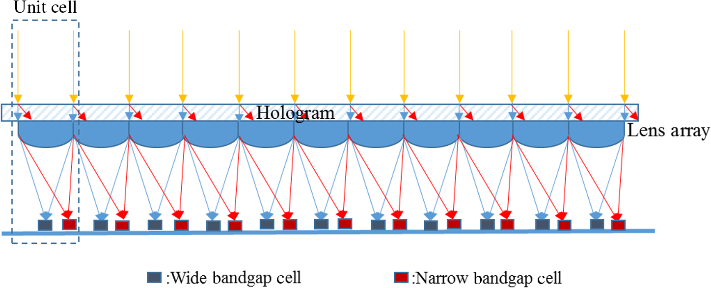
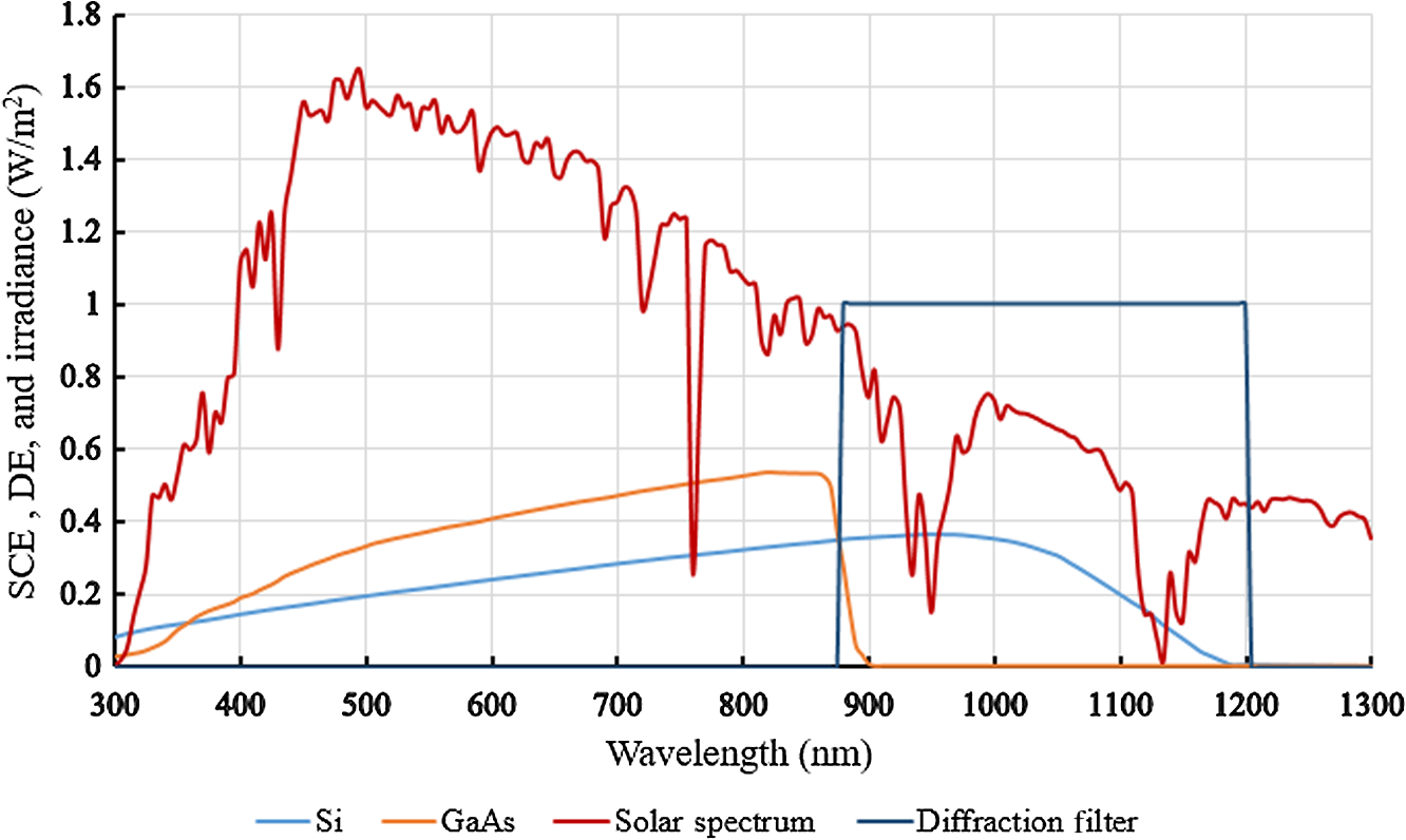
1.IntroductionThe maximum theoretical efficiency of a single bandgap PV cell can reach only 33%.1 This is a result of detailed balance consideration between the fixed solar spectrum power distribution and a converter with a single energy bandgap. This limitation can be removed by using converters with multiple bandgap energies distributed over the solar power spectrum.2 Spectrum-splitting is a multijunction technique that spatially separates spectral components of incident solar illumination and delivers them to PV cells with maximum spectral response to a particular PV cell. Since each bandgap is independent of each other, there is more freedom of bandgap and material selection compared to a tandem PV system.3 In addition, the PV cells are no longer current limited which allows for grater energy yield. However, spectrum splitting shifts the system complexity from the cell fabrication to the optics.4 Both reflective and transmission spectrum splitting systems have been demonstrated.5–10 Reflective spectrum splitting typically uses a set of dichroic filters to separate different wavelength bands; however, transmission configurations can be formed with a single dispersive element and are potentially simpler to design. In transmission configurations, the dispersed spectrum must be focused to improve spectral filtering and spatial separation.11 This can be achieved by either applying a lens after the dispersive element7 or by combining focusing power with the dispersive element.9,10 However, combining both focusing and spectral separation in the diffractive optical element requires higher spatial frequencies. This is especially true if large diffraction angles are required to minimize the separation between the diffractive element and the PV plane. Along with recent developments of spectrum splitting systems, there has been interest in microscale concentrating photovoltaic (MCPV) systems.12–14 These systems reduce the size of a large concentrating PV system into an array of microconcentrating units. Using tandem multijunction PV cells, the system achieved an increased conversion efficiency with a compact flat configuration. MCPV systems can also benefit from compact and less costly microtracking techniques, improved heat rejection properties, and “smart” interconnections of PV cells.15 In this paper, a holographic spectrum splitting microconcentrating photovoltaic (HSSMCPV) array is evaluated that uses a GaAs wide bandgap cell and a silicon narrow bandgap PV cell. A holographic spectrum splitting filter is designed in dichromated gelatin film and the simulated properties of this filter are used to estimate the performance of the HSSMCPV array in combination with published data for the PV cells. Two different -numbers () for the microlenses are examined to illustrate the design issues. The results show a significant improvement in conversion efficiency with the spectrum splitting microconcentrator array using microlenses with due to higher optical efficiency and an overall improvement over nonspectrum splitting microconcentrator arrays. 2.System Design2.1.System StructureThe basic structure of the two-junction HSSMCPV system is shown in Fig. 1. In this design, a planar grating volume hologram is positioned above an array of lens elements to separate the spectral components of the incident light. The volume hologram can efficiently diffract a spectral band into a single order and allow the remaining spectral components to pass directly through the hologram. Each lens in the array focuses both the transmitted and the diffracted light to positions near the optical axis. As shown in Fig. 1, a wide bandgap PV cell is located on the optical axis of each lens, and a narrow bandgap cell is located at the focus of the diffracted beam. In the proposed system, the hologram is designed to diffract a long wavelength light at an off-axis angle to the center of the narrow bandgap PV cells. Light in the zero order is focused onto the wide bandgap PV cell. 2.2.Evaluation MetricsThe performance of a spectrum splitting system can be evaluated in terms of the spectral conversion efficiency (SCE) and quantum concentration ratio (QCR) at each PV cell, the overall power conversion efficiency, the improvement over the performance with the best bandgap PV cell filling the aperture, and the acceptance angle. In this paper, each of these metrics is evaluated for a two-junction HSSMCPV array. The unit cell structure of the proposed HSSMCPV is shown in Fig. 2 and consists of a planar holographic spectrum splitting filter, a refractive microlens, a GaAs PV cell at the optical axis of the lens, and a silicon PV cell at the focus of the diffracted beam. Fig. 2Detailed configuration of the ’th unit cell in the HSSMCPV system and the spectral energy flow. 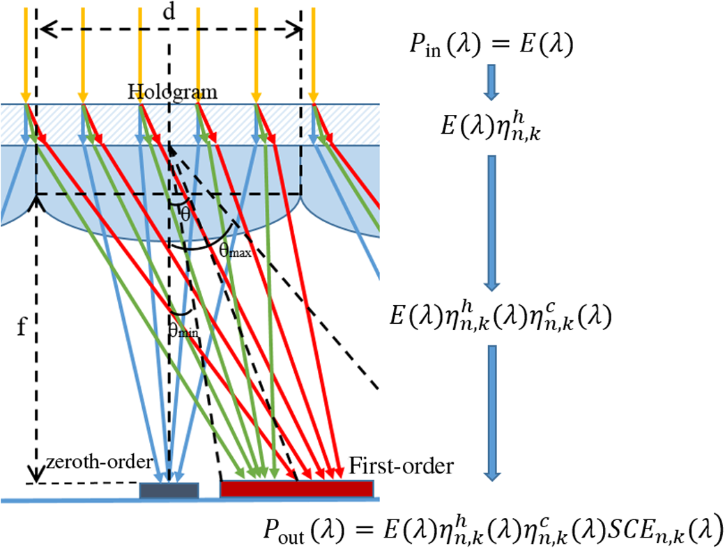 2.2.1.Spectral conversion efficiency and quantum concentration ratioThe SCE of a PV cell specifies the optical to electrical conversion efficiency as a function of wavelength. It is defined as the product of the spectral responsivity (SR), the open circuit voltage (), and the PV cell fill factor (FF) For an ideal spectrum splitting system, the SCE should be significantly different for each PV cell used in the system. Overlapping SCE values reduces the effectiveness of having multiple bandgap PV cells in the system.In a spectrum splitting CPV system, variations in the spectral irradiance that exist at the PV cell surface affect and the SCE over that of a one sun system with uniform illumination. The change in the irradiance in a concentrating system can be quantified as the QCR which can be defined as where is the QCR of the PV cell, and are the currents generated at wavelength with concentration and with one sun illumination, respectively, is the geometrical concentration ratio (GCR) defined as the area of system entrance aperture divided by the PV cell area, is the solar spectral irradiance, is the spectral response of the PV cell, and is the spectral optical efficiency (i.e., the efficiency of the incident illumination spectrum transferred to a particular PV cell in the system). In a single junction CPV system, since the spectral power distributions at the system entrance aperture and at the surface of the PV cell are equal, , and the QCR is equal to the geometric concentration ratio. However, in an HSSCPV system, they are different.Therefore, the SCE of a PV cell in a spectrum splitting CPV system with a QCR of must be redefined to determine the overall system power conversion efficiency. The for this PV cell in the system can be defined as where the and are the spectrum conversion efficiency values under concentration and one sun conditions with an AM1.5G incident spectrum, and are the open circuit voltages under concentration and one sun conditions, FF is the fill factor, is the diode ideality factor, is the Boltzmann’s constant, is the PV cell temperature, and is the electron charge. The SCE with concentration is a combination of the SCE under one sun conditions and a QCR depended increment. Assuming a GaAs cell with , and , and a QCR of 10X, the increment due to concentration is 3.4%.In order to accurately evaluate the two-junction HMSSCPV system, the optical spectral efficiency and the QCR for each bandgap cell are determined using raytracing and diffraction efficiency analysis. These values are then combined with the computed values for to determine the overall power conversion efficiency of the system. 2.2.2.Overall power conversion efficiencyThe efficiency of the ’th PV cell in the ’th unit cell in the system can be expressed as where is the filtered conversion efficiency of the ’th PV cell; is the incident solar illumination spectrum; is the total incident power on a unit cell aperture; is the spectral optical efficiency of the hologram for the spectral band corresponding to the ’th cell; the ratio of the power incident on the microlens to the power received by the ’th cell; and is the SCE of the ’th PV cell with QCR of . The overall system efficiency for the ’th unit with two PV cells is given as and the overall system power conversion efficiency with -unit cells isAn examination of Eqs. (3)–(5) shows two aspects of multijunction systems. First, for one sun system, the narrow bandgap PV cells operate with a reduced SCE, because their averaged QCRs are smaller than 1. The second aspect is that in order to optimize the system performance, the QCR of the higher efficiency PV cell should be maximized, because it is the dominant factor and can provide the most improvement on the power conversion efficiency. Based on the above considerations, the design methodology for realizing a high-efficiency HSSMCPV system is to: (i) use PV cells with the highest for specific spectral bandwidths; (ii) optimize the shape of spectral bandwidth filters to maximize for each part of the incident solar spectrum; (iii) optimize PV cell size, shape, and position for maximum optical efficiency; (iv) maximize the PV cell QCR values; and (v) optimize the optical design of the lenses to minimize aberration and loss due to total internal reflection (TIR). 2.2.3.Improvement over best bandgapAnother evaluation metric for spectrum splitting system is the improvement over the best bandgap (IoBB) PV cell used in the system.16 It compares the power conversion efficiency of a spectrum splitting system to the efficiency of a single bandgap system with the best bandgap PV cell efficiency with the same aperture area and incident spectrum as the spectrum splitting system. The IoBB is defined as If the IoBB is larger than zero, the system benefits from the spectrum splitting compared to a single bandgap system. The magnitude of IoBB also provides an indication of whether the increase in efficiency is significant enough to offset the cost of implementing the more complex spectrum splitting system. 2.2.4.System acceptance angleThe acceptance angle of a concentrating PV system can be defined as the incident angle range over which the conversion efficiency is larger than 85%. The acceptance angle for spectrum splitting concentrating PV system is important because it indicates the accuracy required of the tracking system which has a significant impact on the system cost. Therefore, maximizing the acceptance angle is a desirable design goal. However, for the proposed system, there is a tradeoff between the acceptance angle and the geometric concentration ratio. 2.3.Design MethodologyAs discussed above, the design of a two-junction HSSMCPV system depends on several parameters including the types of PV cells used, hologram parameters, the lens design, and the geometry of the module. 2.3.1.Cell selectionAs discussed in Sec. 2.2.2, the PV cells for a spectrum splitting system should be selected to have the largest SCE value for a specific spectral band. A spectrum splitting system with two different bandgap PV cells and ideal spectral filters will have a maximum power conversion efficiency of For this design, a combination of GaAs and Si PV cells is used since their bandgaps are well separated and have high SCE for both cells. Data for a GaAs and crystalline silicon (Si) cells were selected from the literature.17,18 Table 1 shows the basic PV cell parameters under one sun with AM1.5 spectral conditions. Figure 3 shows the SCE for these cells and also the diffraction efficiency function for an ideal spectral filter. The spectrum splitting system power conversion efficiency computed for these cells in combination with ideal spectral filtering using Eq. (8) was found to be 32.23%. The IoBB computed using Eq. (5) and the higher efficiency GaAs cell is 20.98%.Table 1Electrical data for the selected GaAs and Si solar cells.
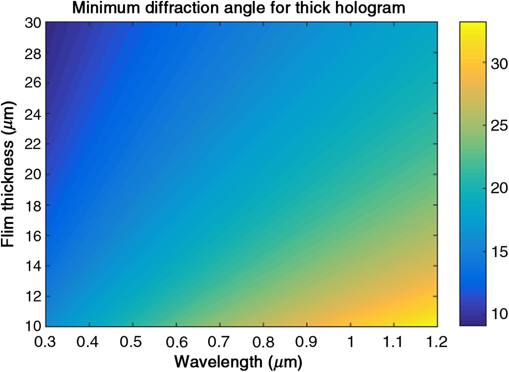
2.3.2.Holographic element designThe first step in designing this volume holographic optical element (HOE) is to determine the filter cut-off wavelength. For a PV cell combination of Si and GaAs, an ideal rectangular spectral filter should direct incident wavelengths from 880 to 1200 nm to the Si cell and allow shorter wavelengths to pass through the hologram and go to the GaAs cell. The hologram diffracts light to the Si cells for two reasons. First, the maximum diffracted spectral bandwidth of a single hologram is which is sufficient to cover wavelengths larger than the cut-off wavelength of the GaAs cell but less than the cut-off for the Si cell (880 to 1200 nm), but not large enough to cover the full absorption band of GaAs (300 to 880 nm). The second advantage is that focusing the transmitted zeroth-order on-axis illumination will have lower aberration than focusing the off-axis diffracted first-order. This allows higher QCR and more uniform illumination on the more efficient and more expensive GaAs cells. Another important design consideration is the hologram diffraction efficiency.19 For a volume hologram, the diffraction efficiency for a single order can approach 100% provided the hologram parameters satisfy certain criteria. In particular, the parameter should satisfy the condition where is the free-space wavelength, is the thickness of the hologram, is the average refractive index of the hologram, and is the volume grating period.The volume grating period is determined by the Bragg condition given by where is the grating vector; and are the propagation vectors of the two incident construction beams; and are the components of the grating period in and directions. If the -direction is along the surface of the grating, then will determine the direction of the first-order diffracted beam and can be found using the grating equation: where and are the angles of the diffracted and incident beams.For normally incident light and considering Eqs. (9)–(11), there is a minimum diffraction angle at the operating wavelength that provides high diffraction efficiency in one order, given by where is the minimum diffractive angle, and is the operating wavelength.In this design, sensitized dichromated gelatin (DCG) film is used for the hologram which has an average refractive index of . Figure 4 is a plot of the minimum diffraction angle as a function of wavelength for different hologram thickness values. The thickness of DCG holograms can be controlled by using different material composition, exposure, and processing parameters. For the design, the diffraction angle must be minimized to reduce aberration and TIR loss of the diffracted beam. A sufficiently thick film must be used to allow a smaller diffraction angle while maintaining the requirement (i.e., ) for high diffraction efficiency. Allowing for these considerations, the minimum diffraction angle for the GaAs cutoff wavelength () is 18.03 deg; and the minimum diffraction angle for the wavelength at the center of the diffracted spectral band () is 19.73 deg; and the minimum diffraction angle corresponding to the Si cell cutoff wavelength () is 20.90 deg. These angle and diffraction efficiency requirements can be satisfied with a hologram thickness of . 2.3.3.Lens array designIn the HSSMCPV system, the lens array is used to concentrate the separated spectral components at the relevant solar cell locations. Different lens shapes and -numbers () may lead to a significant loss in optical efficiency [] due to the TIR loss within the lens. To minimize optical loss, and simplify the configuration, a hexagonal shape planoconvex spherical lens array is chosen for the system. The determines the focusing power of a lens and is equal to , where is the effective focal length, and is the diameter of the lens. In a concentrating PV system, a smaller means a higher geometric concentration ratio and lower spacing requirements. The use of a small lens array reduces system thickness with the same GCR. However, since the red light diffracted by the hologram enters the lens at a large off-axis angle, a thick lens with small can lead to a TIR loss at the edge of the curving surface and significant aberration. Both losses increase as the diffraction angle increases, and the decreases. As a result, there is an optimum for the since a larger value will have lower TIR loss and aberration while a lower will more readily allow the requirement to be satisfied and reduce system volume. In the simulation, two lens arrays with equal to 1 and 1.5 were modeled to satisfy the constraints for the two-junction HSSMCPV system. 2.3.4.Hologram and cell geometriesAnother limitation on the hologram diffraction angle is the system geometry. To some extent, this is determined by restrictions resulting from the lens array fabrication method. Figure 5 shows the top view of the two-junction HSSMCPV system. To maximize the optical efficiency, a hexagonal lens pattern is used with the diffracted light directed to a rectangular narrow bandgap cell (shown in red) that is positioned along the edge of a unit cell. A wide bandgap cell is located at the optical axis of the lens. The largest diffraction angle is set by the longest wavelength (1200 nm) in the desired diffracted spectral band and has a value of where is the separation of each unit array structure in the direction, is the side length of the GaAs PV cells, is the focal length of the lens array. The minimum diffraction angle for 880 nm light isFig. 5Top view of the two-junction HSSMCPV system. The blue hexagons are the microlenses, the blue and red pads below the lens array are the wide and narrow bandgap solar cells. 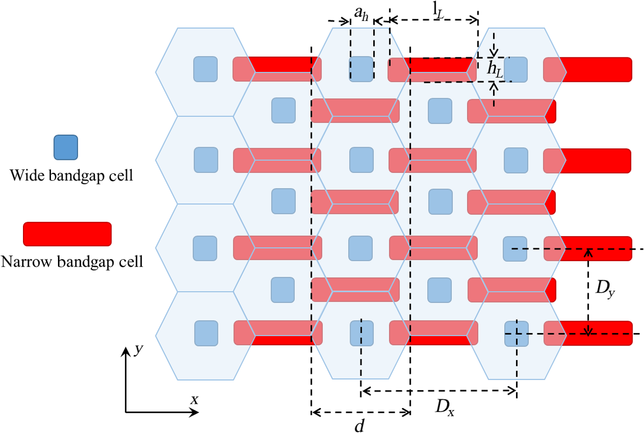 With these conditions, the hologram parameters can be optimized with rigorous coupled-wave analysis (RCWA). A grating profile was optimized using the grating period, the grating slanted angle, swelling parameters, and the index modulation as variables. Two gratings are optimized for the selected systems with lens arrays with and 1.5, and have a diffraction band centered at 1050 nm with diffraction angles of 40 deg () and 30 deg (). The final step in the design of the HSSMCPV system is to determine the PV cell size and location on the receiver plane. These parameters affect both the QCR and the acceptance angle. There is a tradeoff between increasing the power conversion efficiency with high QCR and obtaining a large acceptance angle with larger cell size. For the proposed system, the wide bandgap GaAs PV cells were designed with a square shape located at the center of unit cells to match and collect light in the zeroth-orders. The narrow bandgap Si PV cells have a rectangular shape and are located between two GaAs cells. The size and location of each cell type were optimized to achieve high optical efficiency with an acceptance angle larger than . 2.4.Design ResultsThe parameters for the HSSMCPV systems with microlens arrays with and are given in Table 2. The system geometry and the holographic filters properties are also summarized in Table 2. Table 2Optimized parameters of the system geometry and HOE for each HSSMCPV system.
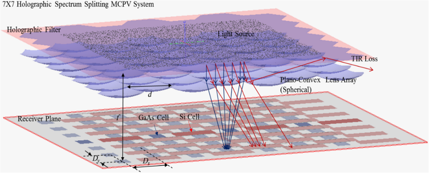
3.Simulation and ResultsThe optical efficiency, power conversion efficiency, QCR, IoBB and acceptance angle as described in Sec. 2.2 were simulated with one sun illumination conditions. A nonsequential raytracing software, Photon Engineering FRED® Optimum,20 is used to simulate the optical properties of the designed systems under different illumination conditions. The diffractive efficiencies for all wavelength and incident angles of the holographic filters were calculated with RCWA software (RSoft DiffractMODMT21). 3.1.Optical ModelTo simulate the optical properties, a system with an array of unit cells is modeled using the nonsequential raytracing software. The system is shown in Fig. 6. The model includes a hologram placed on top of a hexagonal-shaped lens array with corresponding . The GaAs and Si PV cells were modeled as detectors placed at the optimized locations on the focal plane. Solar illumination is modeled as a source plane with the direct AM1.5 solar spectrum placed above the hologram. The diffractive properties of the holographic filter for all wavelengths and incident angles were calculated using the RCWA and assigned to the hologram surface. Rays are then traced from the source plane through the hologram and lens and collected at the detectors that represent the two PV cells. The detectors monitor the spectral power of rays that intercept their surfaces. This information is then used to compute the spectral optical efficiency of each PV cell. The QCR, the for each PV cell, and the total system power conversion efficiency are calculated using Eqs. (2)–(6). 3.2.Holographic FiltersThe holographic elements were modeled and optimized using RCWA. The model was created for a volume transmission hologram formed in DCG. A periodic nonsinusoidal profile was used to model the index variation in the volume hologram. The hologram parameters include the grating periods components in the surface and depth direction, the film thickness, the swelling parameters, and the index modulation. These hologram parameters for DCG material were then optimized to form a hologram with high diffraction efficiency with the desired spectral bandwidth. With this method, holograms for both the and 1.5 systems were optimized to have high diffraction efficiency from 900 to 1200 nm with the required diffraction angles specified in Table 2. The diffraction efficiency for all wavelengths and incident angles was then calculated for different points across the grating surface and used as a weighting function for rays that pass through the system aperture. Figure 7 shows the diffraction efficiency for volume holograms with optimized DCG parameters for the two systems. The results show a bandwidth of 250-nm spectral bandwidth with high diffraction efficiency. 3.3.System PerformanceTable 3 summarizes the simulated system performance for the HSSMCPV systems with ideal filters, optimized DCG holographic filters for the and 1.5 systems. Under the direct AM 1.5 solar illumination, the HSSMCPV system with has the highest power conversion efficiency. It has a system power conversion efficiency of a 31.98% and an IoBB of a 20.05%. The resulting QCR for the GaAs cells is 14.41 and 0.75 for the Si PV cells. The system with shows a better performance than the system because of the reduced TIR loss and aberration degradation. Increasing the further is difficult because the volume hologram cannot reach high efficiency for smaller diffraction angles. Compared with other spectrum splitting systems as described in Refs. 9 and 10, the HSSMCPV system obtains higher geometric and QCRs for each bandgap, and will have higher power conversion efficiency for the same combination of PV cells. Table 3The simulation results for the HSSMCPV systems with ideal filters, hologram filters (HOE) with F/#=1 and 1.5 under the direct AM 1.5 solar illumination. The performance of an ideal combination of GaAs and Si PV cells with no QCR is also shown in the first row for comparison.
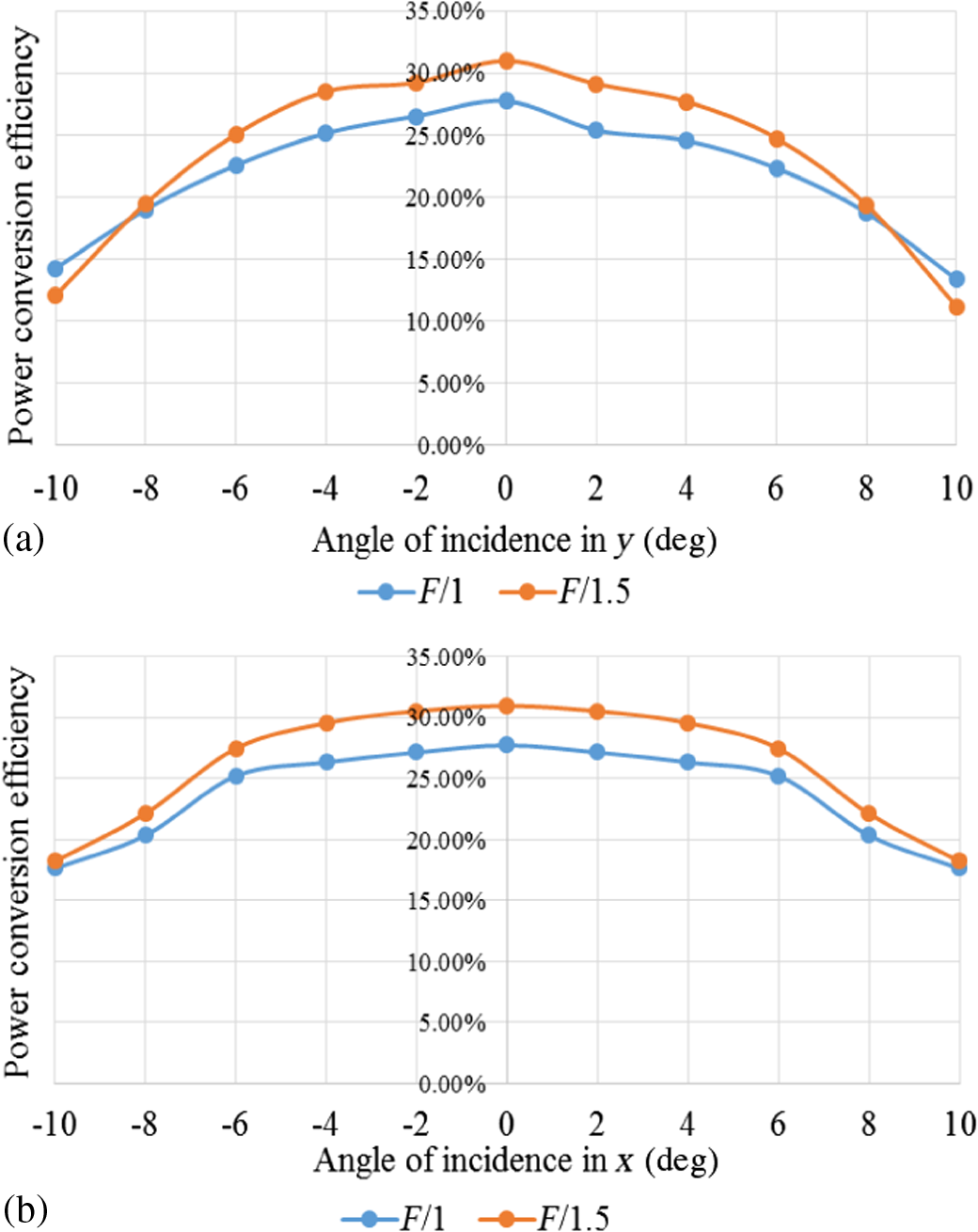
The power conversion efficiencies of the HSSMCPV systems were also simulated with different incident angles to quantify the system acceptance angle values in both and directions. Figure 8 shows the system power conversion efficiencies of the HSSMCPV systems with different incident angles. In the plane corresponding to the primary direction of diffraction by the hologram (i.e., -direction), there are two factors that lead to a decrease in efficiency. First, the Bragg matched or highest efficiency wavelength for the holographic elements changes when the incident angles deviate from the designed angle. Second, when the solar incident angle deviates from the normal, the light in the zeroth-order moves away from the center of GaAs cells. The simulated system acceptance angle in the -direction for the and 1.5 systems are found to be and . In the plane that is perpendicular to the diffraction direction (i.e., -direction), the diffraction properties of the hologram decrease more slowly with changes in incident angle. In this direction, the acceptance angles of and 1.5 systems are found to be and . 4.ConclusionsThe design and performance of a two-junction spectrum splitting MCPV system was described that obtains high power conversion efficiency in a compact system module. A detailed analytical model for a spectrum splitting system was developed to evaluate the spectrum splitting system. The important parameters that were evaluated in the design include the QCR, power conversion efficiency, IoBB, and acceptance angle. The methodology for designing the two-junction HMSSCPV system includes consideration of the system geometry, holographic filter, and microlens design. Two HSSMCPV systems were evaluated with lens arrays having and 1.5. Holographic filters were optimized using parameters DCG films and provide an average diffraction efficiency of 90% over a spectral band ranging from 900 to 1200 nm. The filtering properties of the holograms were used in combination with published data for GaAs (26.64% efficient) and silicon (21.07% efficient) PV cells to simulate the performance of the HSSMCPV with the two different . The simulation showed that the system with reached a higher power conversion efficiency of 31.98% under direct AM 1.5 solar illumination which is an improvement of 20.05% compared to a system with the same aperture using only the higher efficiency GaAs cell. Acceptance angles of and were obtained in the two orthogonal directions for the system with . In addition, the HSSMCPV module is relatively thin (25 mm) compared to conventional CPV systems with the same (i.e., 1.5 m for a circular aperture concentrator with a diameter of 1 m) and can be readily scaled to large areas. AcknowledgmentsThe authors wish to acknowledge support from the NSF/DOE ERC cooperative agreement No. EEC-1041895, NSF Grant No. ECCS-1405619. ReferencesW. Shockley and H. J. Queisser,
“Detailed balance limit of efficiency of p-n junction solar cells,”
J. Appl. Phys., 32
(3), 510
–519
(1961). http://dx.doi.org/10.1063/1.1736034 Google Scholar
A. Barnett et al.,
“Very high efficiency solar cell modules,”
Prog. Photovoltaics Res. Appl., 17
(1), 75
–83
(2009). http://dx.doi.org/10.1002/pip.v17:1 Google Scholar
L. Z. Broderick et al.,
“Design for energy: modeling of spectrum, temperature and device structure dependences of solar cell energy production,”
Solar Energy Mater. Solar Cells, 136 48
–63
(2015). http://dx.doi.org/10.1016/j.solmat.2014.12.034 SEMCEQ 0927-0248 Google Scholar
A. L. Gray et al.,
“Multi-terminal dual junction InGaP2/GaAs solar cells for hybrid system,”
in 33rd IEEE Photovoltaic Specialists Conf. (PVSC ‘08),
1
–4
(2008). http://dx.doi.org/10.1109/PVSC.2008.4922575 Google Scholar
J. D. McCambridge et al.,
“Compact spectrum splitting photovoltaic module with high efficiency,”
Prog. Photovoltaics Res. Appl., 19
(3), 352
–360
(2011). http://dx.doi.org/10.1002/pip.1030 Google Scholar
D. Zhang et al.,
“Reflection hologram solar spectrum-splitting filters,”
Proc. SPIE, 8468 846807
(2012). http://dx.doi.org/10.1117/12.929187 PSISDG 0277-786X Google Scholar
J. M. Russo et al.,
“Grating-over-lens concentrating photovoltaic spectrum splitting systems with volume holographic optical elements,”
Proc. SPIE, 8821 882106
(2013). http://dx.doi.org/10.1117/12.2026020 PSISDG 0277-786X Google Scholar
B. Mitchell et al.,
“Four-junction spectral beam-splitting photovoltaic receiver with high optical efficiency,”
Prog. Photovoltaics Res. Appl., 19
(1), 61
–72
(2011). http://dx.doi.org/10.1002/pip.v19.1 PPHOED 1062-7995 Google Scholar
S. D. Vorndran et al,
“Off-axis holographic lens spectrum-splitting photovoltaic system for direct and diffuse solar energy conversion,”
Appl. Opt., 55 7522
–7529
(2016). http://dx.doi.org/10.1364/AO.55.007522 APOPAI 0003-6935 Google Scholar
P. Wang et al.,
“A new class of multi-bandgap high-efficiency photovoltaics enabled by broadband diffractive optics,”
Prog. Photovoltaics Res. Appl., 23
(9), 1073
–1079
(2015). http://dx.doi.org/10.1002/pip.v23.9 Google Scholar
J. Russo et al.,
“Cross-correlation analysis of dispersive spectrum splitting techniques for photovoltaic systems,”
J. Photonics Energy, 5
(1), 054599
(2015). http://dx.doi.org/10.1117/1.JPE.5.054599 Google Scholar
B. Furman et al.,
“A high concentration photovoltaic module utilizing micro-transfer printing and surface mount technology,”
in 35th IEEE Photovoltaic Specialists Conf. (PVSC ‘10),
000475
–000480
(2010). http://dx.doi.org/10.1109/PVSC.2010.5616766 Google Scholar
B. H. Jared et al.,
“Micro-concentrators for a microsystems-enabled photovoltaic system,”
Opt. Express, 22
(S2), A521
–A527
(2014). http://dx.doi.org/10.1364/OE.22.00A521 OPEXFF 1094-4087 Google Scholar
G. N. Nielson et al.,
“Microfabrication of microsystem-enabled photovoltaic (MEPV) cells,”
Proc. SPIE, 7927 79270P
(2011). http://dx.doi.org/10.1117/12.876422 PSISDG 0277-786X Google Scholar
S. Paap et al.,
“Cost analysis for flat-plate concentrators employing microscale photovoltaic cells,”
in IEEE 39th Photovoltaic Specialists Conf. (PVSC ‘13),
3431
–3434
(2013). http://dx.doi.org/10.1109/PVSC.2013.6745185 Google Scholar
J. M. Russo et al.,
“Spectrum splitting metrics and effect of filter characteristics on photovoltaic system performance,”
Opt. Express, 22
(S2), A528
–A541
(2014). http://dx.doi.org/10.1364/OE.22.00A528 OPEXFF 1094-4087 Google Scholar
B. M. Kayes et al.,
“27.6% conversion efficiency, a new record for single-junction solar cells under 1 sun illumination,”
in 37th IEEE Photovoltaic Specialists Conf. (PVSC ‘11),
000004
–000008
(2011). Google Scholar
M. A. Green et al.,
“Solar cell efficiency tables (version 45),”
Prog. Photovoltaics Res. Appl., 23
(1), 1
–9
(2015). http://dx.doi.org/10.1002/pip.v23.1 Google Scholar
H. Kogelnik,
“Coupled wave theory for thick hologram gratings,”
Bell Syst. Tech. J., 48
(9), 2909
–2947
(1969). http://dx.doi.org/10.1002/bltj.1969.48.issue-9 BSTJAN 0005-8580 Google Scholar
“FRED optimum software,”
(2015) http://www.photonengr.com/software/ June ). 2015). Google Scholar
“DiffractMOD product overview,”
(2015) http://optics.synopsys.com/rsoft/rsoft-passive-device-diffract June ). 2015). Google Scholar
BiographyYuechen Wu received his Bachelor of Science degree in electrical and computer science engineering at the University of Toledo in 2012. He is currently pursuing a PhD in electrical and computer engineering, and working at the Photonic System Laboratory at the University of Arizona. His research interests include diffractive optics, optical engineering, micro-optics, and solar energy. Raymond K. Kostuk has a joint professor position with UA’s ECE Department and the College of Optical Sciences. He received a PhD in electrical engineering from Stanford University. His primary area of expertise is in holographic concepts, materials, and applications, with over 30 years of experience in that area. He is a fellow of the Optical Society of America and SPIE. |