|
|
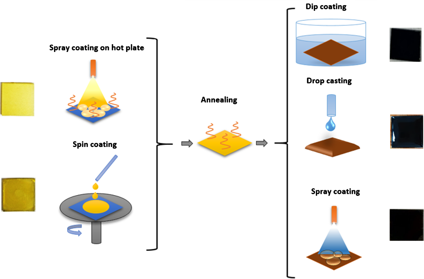
1.IntroductionInorganic (e.g., chalcogenide), organic (e.g., polymeric), mixed inorganic-organic (e.g., perovskite), and quantum-dot thin film solar cells (SCs) are in the forefront of research and development in energy and nanotechnology fields to secure a renewable and cost-effective source of electrical energy based on the photovoltaic (PV) effect.1,2 The aforementioned PV SCs have the potential to be fabricated using low-cost vacuum-free techniques, such as processing and casting from solutions. Organometallic perovskite SCs (PVSCs) are currently the most attractive in the abovementioned list with compelling efficiencies over 20%,3 and therefore are the focus of this work. A recent review of the structure and advances in PVSCs is found in Ref. 2. The perovskite light harvesting layer in a PVSC may be formed using a two-step sequential deposition strategy4,5 or a one-step approach.6,7 In the two-step sequential deposition, the perovskite layer, e.g., methylammonium lead iodide (), is prepared in two steps. First, the precursor solution is deposited on the substrate by a casting method, preparing a thin layer composed of crystals. Then, this layer is exposed to the solution of (MAI) to form perovskite crystals in a film. In the one-step approach, a mixture of and dissolved in appropriate solvents is directly deposited on the substrate. Grätzel et al.4 introduced the two-step sequential deposition method as a replacement for the one-step deposition in order to achieve a better control over the perovskite film morphology. Indeed, they fabricated nearly pinhole-free perovskite films using this method. Since then, the method has been continuously improved by others using various strategies, such as vapor deposition of the two precursors8 or well-controlled two-step spin coating.9 Currently, the two-step sequential deposition of perovskite precursors is usually performed by spin-spin or spin-dip coating, whereas spin-coating is usually used in the one-step method. The process of film deposition may affect the film morphology, nanostructure, and optoelectronic properties, and consequently the device performance. Application of spin coating is limited to small areas in a batch process, not suitable for real-world applications.10 Therefore, in parallel to attempts to further improve the power conversion efficiency (PCE) and stability of PVSCs, it is also essential to develop scalable techniques for future commercialization of the technology. There are essentially a limited number of scalable techniques that can be employed to fabricate solution-processed thin films in PV and organic electronics, including spray coating, inkjet printing, slot-die coating, doctor balding or knife over edge, drop casting, gravure, and screen-printing.5,10,11–14 Spray coating has been widely used for the fabrication of other emerging SCs, e.g., Refs. 1516.17.18.19.–20, but has not been adequately explored in the PVSC field, and only a few studies have employed it to fabricate the perovskite layer.21–33 Due to the stochastic and random nature of droplet impact, spray-on films normally show a rough surface,21 but the roughness can be reduced through a process optimization.22,28 High roughness in spray-on organic SCs was reported to have negative effect on the light absorbance10 and the device fill factor (FF),34 although the results obtained for the organic SCs may not be necessarily applicable to crystalline perovskite SCs. By controlling the process parameters, such as substrate temperature, spray flow rate, number of spray passes, and solution concentration,11,19,20,22,23,32,35 or applying dynamic forces on the substrate, such as ultrasonic vibration2,5 or mechanical force (pressing),22 the spraying process may become controllable to some extent. In some recent works, progress has been made toward fabrication of high efficiency spray-on SCs in both organic and perovskite devices.22,36,37 Spray coating of perovskite, compared to polymeric thin films, imposes additional challenges due to the crystalline nature of perovskite and crystal formation during the process, which may cause crystallization dewetting.13 An incomplete and dewetted perovskite layer with excessive pinholes and voids may create shunt pathways,24 causing charge recombination and a decline in the device performance.21 Following the foregoing introduction and argument, in this paper, spin and dip coating, used in the sequential method, are replaced by scalable spray coating and touch-free drop casting methods. To be more specific, will be deposited by spray coating and the process will be optimized, then the MAI solution will be deposited atop the film by spray coating and also drop casting. To enhance the coverage, multiple pass spraying strategy is employed, and the effect of the number of spray passes on the film characteristics is studied. Then by controlling the solution concentration and optimizing the speed of the spray, the distance of the nozzle from the substrate, and the substrate temperature, a fully-covered perovskite film is obtained. The perovskites made by these methods are characterized and used to prepare PVSCs with the n-i-p structure of fluorine-doped tin oxide (FTO)-coated , where spiro-OMeTAD is the short form for 2,2′,7,7′-Tetrakis[-di(4-methoxyphenyl)amino]-9,9′-spirobifluorene, and is a compact layer of . Figure 1 shows the schematic diagram of the casting methods used in this work to fabricate the perovskite layer in a two-step sequential process. 2.Experimental Details2.1.Materials and MethodsLead iodide (, 98.5%), -dimethylformamide (DMF, 99.8%), hydrogen chloride (HCl, 37.5%), ethanol (99.9%), toluene (98.8%) and titanium (IV) isopropoxide (97%), spiro-OMeTAD, 4-tert-butylpyridine (96%), acetonitrile (99.8%), and bis(tri-fluoromethane)sulfonamide lithium salt (99.95%) were purchased from Sigma-Aldrich. Methylammonium iodide (MAI, 99.5%) was purchased from Xi’an Polymer Light Technology Co, China. For optimization and characterization purposes, FTO-coated glass substrates were used, whereas for device fabrication, substrates were used and etched by zinc powder and HCl solution to achieve a desired pattern. The substrates were washed in deionized water and soap solution, acetone, and isopropyl alcohol by sonication, and then treated in UV–ozone cleaner for 20 min. The electron transporting layer was fabricated by spinning the precursor solution on FTO-coated glass at 2000 rpm for 60 s, followed by annealing at 500°C for 1 h. To prepare the precursor solution, of HCl (2M) was diluted in 2 ml of ethanol and then this solution was added to titanium isopropoxide solution dropwise under stirring condition. Titanium isopropoxide solution was prepared by dilution of of titanium isopropoxide in 5 ml of ethanol. The perovskite layer () was formed atop the layer in a two-step sequential process. First, the film was fabricated through spray coating, as well as spin coating, as the reference method. For the spun-on films, was dissolved in DMF in four molarities of 0.2, 0.5, 0.7, and 1 M, and the solution was spun at 2000 rpm for 30 s. Then the film was annealed at 90°C for 30 min. The spray-on films were fabricated using 0.7 M solution of (323 mg of dissolved in 1 ml of DMF). Before use, the solutions were heated at 60°C for 1 h and then cooled at room temperature. Spray coating of film was conducted using a spray-coating machine (Holmarc Opto-Mechatronics Pvt. Ltd., Model HO-TH-04, Kerala, India) in air, using air-assist spray nozzle. The flow rate was kept constant at and the spray nozzle atomization air pressure was tuned at 2 bars. Other spray parameters including the height (nozzle–substrate distance), the speed of the nozzle movement over the substrate (or speed of substrate movement with respect to a stationary nozzle), the number of spray passes, and temperature of the substrate were varied to find the optimum values for the best film characteristics. To mimic the real situation in PVSC fabrication, for the optimization process, all films were deposited onto FTO-coated . During spray coating of , the substrate temperature was set at specific values. Finally, all samples were transferred to an oven for annealing at 90°C for 30 min. In the second step, dip coating, spray coating, and drop casting were used to deposit the MAI solution. In dip-coating experiments, some spun-on and spray-on samples were dipped in 2 ml of MAI solution, for 5, 20, or 60 min (MAI was dissolved in 2-propanol to obtain concentration of ). In drop casting experiments, of the MAI solution was dripped on films from 2 cm above the film each time. This process was repeated every 5 min to obtain various samples for further analysis. In the experiments where spray coating was used as the method for deposition of the MAI solution, a small spray gun placed in the glovebox was used. This was done because spray coating of MAI in air resulted in decomposition of perovskite. The spray gun was kept at an optimum distance of 5 cm from the samples. A total of 2 ml of the MAI solution was deposited by pulsed-spray coating for 20 min, in time intervals of 1 min to allow sufficient time for solvent evaporation. In each pulse, of MAI solution was sprayed on the film within 1 s, which wetted the film completely. All perovskite samples made using various methods were put on a hotplate in the glovebox and annealed at 90°C, for 2 h. Spiro-OMeTAD solution was prepared by mixing 60 mg of spiro-OMeTAD, of the lithium salt in acetonitrile, and of 4-tert-butyloyridine. The solution was deposited atop the perovskite layer through spin coating in the glovebox at 2000 rpm for 30 s, and the samples were kept there for 12 h. To complete the device, 100 nm of gold was thermally evaporated atop the spiro-OMeTAD film. The devices were encapsulated using glass and UV-treated epoxy. The samples were partially exposed to high ambient humidity (50% to 70%) during transfer from the glovebox to the thermal evaporator as well as during the device encapsulation. 2.2.Film and Device CharacterizationOptical microscopy images of films were taken by a confocal laser scanning microscope (CLSM 700, ZEISS, Oberkochen, Germany) at magnification of () and (), while scanning electron microscopy (SEM, Hitachi, Model S-3400N, Japan) was used to study the surface topography of perovskite films. Optical images with magnification of were imported to ImageJ software to analyze and estimate the coverage of and perovskite films. Film thickness and profile roughness (Ra: arithmetic average of peaks and valleys) were measured using a stylus profiler (KLA-Tencor P7). To measure the roughness, random lines with a length of at least 1 mm were selected on the surface of each sample. The film thickness was measured with respect to the cleaned edges of the samples. Coverage, roughness, and thickness experiments were run in triplicate. X-ray diffraction (XRD, model D5005, Bruker, Germany) analysis was performed to study the crystal structure of the perovskite films. UV-visible absorbance spectra of perovskite films were obtained using UV-vis spectrophotometer (EV300, Thermo Fisher Scientific, Waltham, Massachusetts). Photoluminescence (PL) characterization was performed using PTI-QM/TM/IM PL spectrometer with PL-F2X nitrogen laser as the excitation source. The PV parameters of the fabricated devices ( curves) were measured by a Keysight source meter Model B2902A, Japan, in the forward direction with normal mode scan speed and under AM1.5G solar irradiation with an intensity of . Before the test, the light intensity was calibrated using a standard Si SC. 3.Results and Discussion3.1.PbI2 FilmsThe first step in two-step sequential fabrication of a perovskite layer is to prepare a uniform film with high coverage to work as a template for the formation of perovskite crystals. As the first step, the concentration of solution was optimized. Figures 2(a)–2(d) show optical images of spun-on films, prepared at various concentrations, and SEM images of their corresponding perovskite films, made by spin-dip coating. Figure 3 shows the thickness and roughness of the films and quantitative values of the coverage of and perovskite films prepared at various concentrations of the solution. Figure 2 shows that large crystals form at a concentration of 1 M. Although this concentration has been frequently applied in mesoporous structures,9,38 it is found that this concentration is not suitable for planar structures. On the other hand, the uniform and fully covered spun-on film prepared using 0.2 M solution shows excessive voids in the corresponding perovskite film, due to the lack of sufficient . Therefore, the solution concentrations of 0.5 and 0.7 M are desirable, albeit at 0.5 M, the corresponding perovskite film shows a lower coverage than that of the 0.7 M. Figure 3 shows that as the concentration of solution increases, the roughness and thickness of the film increases almost linearly. The coverage of the film decreases as the solution concentration increases, because larger crystals form at a higher concentration, resulting in crystallization dewetting.13 It appears that the coverage of perovskite films depends on high or adequate coverage of the film (achieved at concentration of 0.5 and 0.7 M), and the presence of sufficient for a satisfactory conversion of precursors into perovskite. In agreement with this argument, Fig. 3(c) shows that the highest coverage of perovskite is obtained at solution concentration of 0.7 M. It is noted that with a change in spin-coating conditions and thus the film thickness, the optimum concentration may change. Fig. 2Optical images of spun-on films fabricated at various solution concentrations. (a) 0.2, (b) 0.5, (c) 0.7, and (d) 1 M solution. The SEM inset images show the corresponding spin-dip perovskite films. 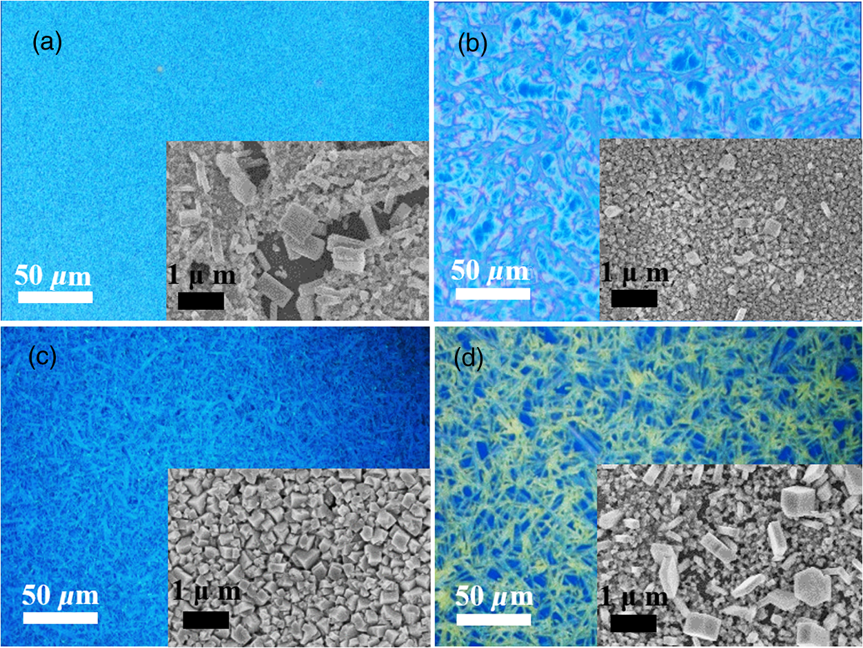 Fig. 3Variation of (a) roughness and (b) thickness of spun-on films against in DMF solution concentration, and (c) coverage of spun-on films and their corresponding spin-dip perovskite films versus concentration of solution. The solutions were spun at 2000 rpm, for 30 s.  Having found the optimum concentration of solution for the highest coverage of spun-on ( to 0.7 M) and spin-dip perovskite films (), spin coating was then replaced by spray coating. Our preliminary experiments showed that the application of multiple spray passes while the substrate is kept at ambient temperature may have a disruptive effect on the morphology of the entire film, because the forthcoming spray passes may disturb the existing wet film. To support this argument, Fig. 4 shows the effect of the number of spray passes (1 and 3 passes) on the morphology of the perovskite films, prepared after dipping the spray-on films into the MAI solution, where the spray nozzle height and speed were kept at 10 cm and , respectively, the substrate temperature was kept at ambient temperature of 25°C, and the solution concentration was set to 0.5 M. At room temperature, increasing the number of spray passes from 1 to 3 results in an increase in the film roughness and thickness that may cause low conversion of to perovskite, because a high thickness hampers penetration of the MAI solution into the lower parts of the film. This hypothesis is backed by the XRD patterns of Fig. 5, showing the peaks of the perovskite made using the spray-dip method, at one and multiple spray passes (spray ; ; and substrate ). The first peak observed in the film made using four passes, around 12 deg, belongs to , which is not observed in the pattern of fully converted perovskite film made using one pass. The peaks near 14.2 deg and 28.6 deg in both graphs are associated with the perovskite structure. Fig. 4SEM images of perovskite films and optical images of their corresponding films (inset), using (a) one spray pass and (b) three spray passes. concentration = 0.5 M; spray nozzle height = 10 cm; ; substrate temperature = 25°C; and dipping time = 1 h. 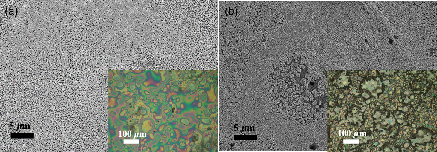 Fig. 5Effect of the number of spray passes on perovskite conversion. XRD patterns of perovskite films prepared using spray-dip coating, showing high conversion (one spray pass) and incomplete conversion (four passes). * represents and # represents perovskite peaks. concentration = 0.7 M; spray nozzle height = 10 cm; ; substrate temperature = 25°C; and dipping time = 1 h. 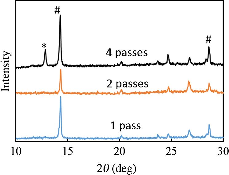 Although the film prepared using one pass shows a high coverage at the first glance (c.f. Fig. 4), pinholes due to partial crystallization dewetting are observed in the film. Figures 2 and 3 had shown that a concentration of to 0.7 M is favorable. Therefore, in another series of experiments, the concentration of film was set to 0.7 M, while spray speed and height of the nozzle were tuned to optimum values to avoid the formation of thick wet films. For the spray nozzle and flow rate used in this study, we found that the optimum spray height is in the range of 12 to 14 cm, and the optimum spray nozzle speed is about . For other sprays, a similar procedure may be followed to arrive at similar conclusions.39 It is found that in ambient temperature, a prolonged drying time may lead to dewetting of the liquid film due to growth of the hydrodynamic perturbations, as well as crystallization dewetting during solvent evaporation.13 To overcome this problem, the substrate temperature may be increased to decrease the film drying time to cure and solidify the film before the perturbations grow and destabilize the thin liquid film. Elevated temperature and rapid solidification may control the crystallization dewetting as well by arresting excessive growth of the crystals. Following the aforementioned argument on the effect of the substrate temperature, the substrates were heated to several temperatures below the boiling point of DMF (153°C), including 40°C, 50°C, 60°C, 75°C, and 100°C, and a temperature near the boiling point of DMF, i.e., 160°C and a temperature higher than the boiling point of DMF, i.e., 200°C. Figure 6 shows the optical images of spray-on films, made at the aforementioned temperatures using one and two spray passes, while other parameters are kept constant at the optimum conditions (i.e., spray nozzle height and speed of 12 cm and , respectively). Figure 7 shows the effect of the substrate temperature on the estimated percentage of the coverage of spray-on films. Figures 6 and 7 collectively show that the coverage of spray-on films increases with the substrate temperature and declines again at temperatures higher than the solvent boiling point and close to the Leidenfrost temperature. One observation is that at low substrate temperature (25°C), a second spray pass severely deteriorates the film coverage, whereas at elevated temperatures, generally, the application of a second spray pass results in a slightly higher or comparable coverage. These findings are interpreted as follows. In spray coating, impinged droplets spread, making liquid disks or lamellae. At ambient temperature, merging or coalescence of some of these disks that are in close proximity to one another may form a wet film or several patches or islands. If the spray flow rate is sufficiently high and droplets impact the substrate rather uniformly, a complete wet film may form through merging of the aforementioned liquid islands. If the flow rate is lower than that required to form a wet film, increasing the number of spray passes delivers more liquid to the substrate, but at the same time disturbs the film. Additionally, in our previous study,13 we demonstrated that large crystals of may form due to the crystallization dewetting. Therefore, a second pass at low substrate temperature may further contribute to the formation of larger crystals and crystallization dewetting. This is clearly observed in images of Fig. 6(a) and also Fig. 7 for the substrate temperature of 25°C. At elevated temperatures, the impinged solution droplets may dry before complete spreading and coalescence with adjacent droplets, preventing the formation of a wet film. The elevated temperature and rapid solvent evaporation also stop excessive crystal growth and the extent of crystallization dewetting. In summary, at elevated temperatures, the second spray pass helps in filling the dewetted areas of the first pass, whereas at room temperature, the second pass disturbs the wet film of the first pass and deteriorates the film coverage. As the substrate temperature approaches the boiling point of DMF (153°C), the film becomes more continuous. Figures 6 and 7 show that the best coverage occurs using one spray pass at temperatures of 100°C and 160°C, in which the impinged droplets dry after adequate spreading. As the temperature increases further (200°C), the coverage is deteriorated because of insufficient spreading. Moreover, the solvent may partially evaporate before impingement causing a decrease in droplet size.39 Also, at high substrate temperatures, close to the solvent Leidenfrost temperature, rapid evaporation of solvent upon impact and the formation of a vapor layer may cause droplet deflection, which disturbs droplet spreading resulting in a low coverage.40 Fig. 6Optical images of spray-on films fabricated using one spray pass (main images) and two spray passes (inset) at substrate temperatures of (a) 25°C, (b) 40°C, (c) 50°C, (d) 60°C, (e) 75°C, (f) 100°C, (g) 160°C, and (h) 200°C. solution concentration = 0.7 M; spray nozzle height = 12 cm; and . 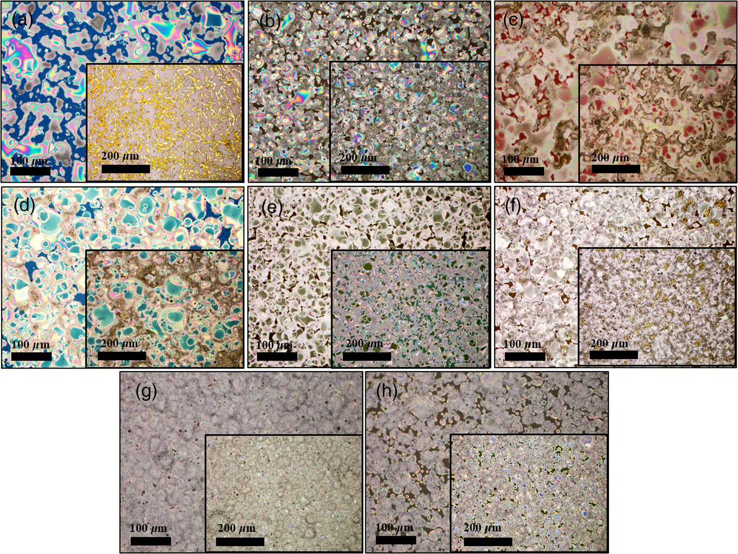 Fig. 7Effect of substrate temperature on the estimated coverage of spray-on films, fabricated using one and two spray passes. concentration = 0.7 M; spray nozzle height = 12 cm; and .  Figure 8 displays the XRD patterns and SEM images of perovskite films made using two-step sequential spray-dip coating. The at concentration of 0.7 M was sprayed using one pass at optimum conditions. In spite of obtaining the highest coverage at substrate temperatures of 100°C and 160°C using one spray pass (Figs. 5 and 6), the XRD patterns of the resulting perovskite films shown in Fig. 8 clearly illustrate a low conversion of to perovskite, for the cases where was deposited at high substrate temperatures of 75°C and 100°C. In other words, crystals processed at elevated temperatures have not adequately converted to perovskite. This may be due to partial sintering and hardening of crystals at elevated temperatures, also resulting in elimination of grain boundaries and crystal interfaces in the film. The hardened crystals with few grain boundaries cannot be easily infiltrated by the MAI solution. Figure 8 shows that full perovskite conversion only occurs at a temperature of 50°C. On the other hand, according to Fig. 7, substrate temperatures lower than 100°C cannot result in a fully covered spray-on film, but increasing the number of spray passes may improve the coverage, provided that the substrate is heated. Thus, overall, the coverage of films sprayed in two passes is better than those deposited using one spray pass. Although the film fabricated using two spray passes at 50°C shows a better coverage (95%) than that with one spray pass (90%) (Fig. 7) and conversion (Fig. 8), its roughness and thickness are higher compared to the film fabricated using one pass (Fig. 9). Therefore, there must be a trade-off between coverage, roughness, and conversion to specify the optimum conditions for the fabrication of spray-on films. The optimum parameters are identified as a substrate temperature of around 50°C, and two spray passes to achieve the best film in terms of coverage, conversion, and uniformity. Figure 9 shows that the perovskite sample made using three spray passes is rough and thick and not favorable. It is noted that the spray flow rate and concentration of solution obviously are important parameters. The spray flow rate should be carefully selected to deliver adequate solution to the film to ideally facilitate the formation of a continuous thin liquid film. As mentioned before, suitable concentration of in DMF and spray flow rate were identified as 0.7 M and , respectively. Fig. 8XRD patterns of spray-dip perovskite films fabricated using spray-on films at substrate temperature of 50, 75, and 100°C, and their corresponding SEM images. * represents and # represents perovskite peaks. concentration = 0.7 M; spray nozzle height = 12 cm; ; and dipping time = 1 h.  Fig. 9Thickness, roughness, and coverage of spray-on and spun-on films. concentration = 0.7 M; spray nozzle height = 12 cm; and . 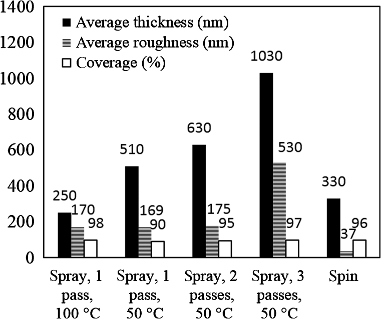 PL spectra of perovskite films, deposited on film by spray-dip coating, are shown in Fig. 10 to demonstrate the importance of coverage in charge collection in PVSCs. Both perovskite films have an emission peak at 773 nm. Lack of full coverage in the sample prepared using one spray pass causes lower extraction of electrons from the perovskite film, which results in a higher PL intensity, in agreement with a similar work22 on mixed halide perovskites sprayed using the one-step method. It is noted that the two films have different thicknesses, i.e., the high coverage film prepared using two spray passes has a higher thickness compared to the low-coverage film prepared using one spray pass. As shown later in this paper, the absorbance is affected by the fabrication process and, therefore, the thickness. Thus, to be more precise, both coverage and thickness affect the PL, although it is deduced that coverage has the main effect. Fig. 10The effect of the film coverage on the PL spectra of perovskite films made on films, using spray-dip coating. The low coverage film (83%) was made using one spray pass on a substrate kept at 25°C, while the high coverage film (95%) was made using two spray passes on a substrate kept at 50°C. concentration = 0.7 M; spray nozzle height = 12 cm; ; and dipping time = 1 h. 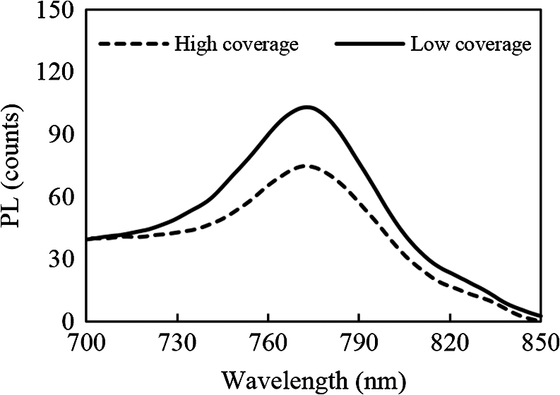 3.2.Spray-on Versus Spun-on PbI2 FilmsIn this section, the characteristics of spray-on films are compared with their lab-scale spun-on counterparts to reveal the merits and potential of spray coating. Figure 9 shows that the thickness of the film made using one spray pass at 100°C is less than that of the spun-on sample, but the thicknesses of the films made using one, two, and three spray passes at 50°C are higher than that of the spun-on film. The roughness values reveal that spray-on films in all the conditions are rougher than spun-on films; nevertheless in all cases the coverage is as high as 90% or higher. Conversion of to perovskite made using spray-dip and spin-dip methods is studied by XRD patterns shown in Fig. 11(a), where a complete conversion is observed in both cases. Additionally, Figs. 11(b) and 11(c) show the optical images of spun-on and spray-on films, and SEM images of the corresponding spin-dip and spray-dip perovskite films, where comparable morphologies are observed, substantiating the merit of spray coating. Fig. 11(a) XRD patterns of spray-dip and spin-dip perovskite films, (b) SEM image of spin-dip perovskite and optical image of the corresponding spun-on film (inset), and (c) SEM image of spray-dip perovskite and optical image of the corresponding spray-on film (inset), prepared using two spray passes. concentration = 0.7 M; substrate temperature = 50°C; spray nozzle height = 12 cm; ; number of spray passes = 2; and dipping time = 1 h. # in XRD patterns represents the perovskite peaks. The height of the films in optical images is not to scale. 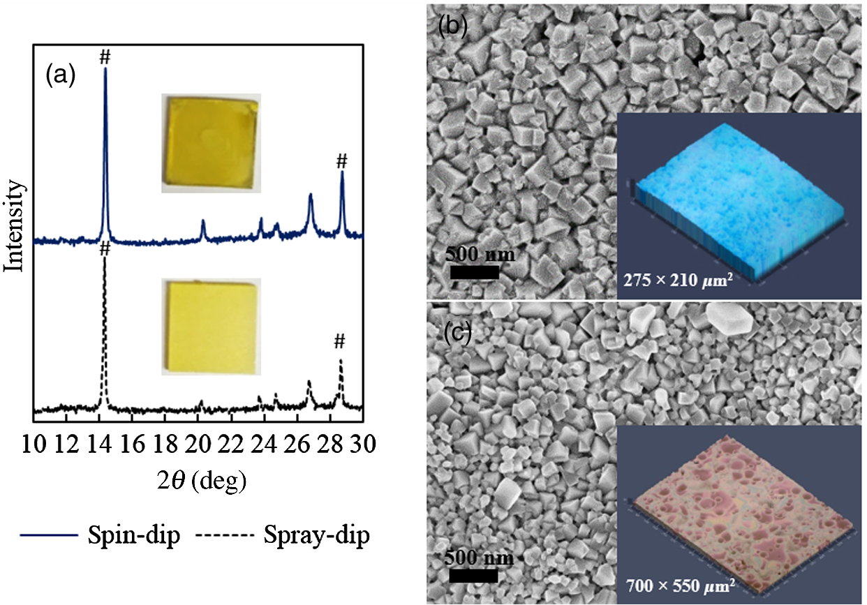 3.3.Perovskite FilmAfter achieving optimum conditions for the fabrication of films by spray coating, through investigating the characteristics of the resulting perovskite films made by spray-dip coating, in an attempt to replace the lab-scale dip coating with scalable methods, here we investigate the application of drop casting and spray coating for deposition of the MAI solution atop spun-on films. In dip coating, 2 ml of MAI solution was consumed to convert spun-on film to perovskite. In drop casting, of MAI was dripped on each sample in 5 min time intervals until full conversion was achieved. The XRD patterns in Fig. 12 show that full conversion of to perovskite is achieved after 20 min in all three techniques by appearance of peaks at 14.2 deg and 28.6 deg, which correspond to (110) and (220) planes of perovskite structure. To spray the MAI solution atop the spun-on films, a pulsed-spray technique was used to allow for solvent evaporation during multiple pulses. For this purpose, of MAI solution was sprayed in 1 s. This process was repeated for 20 times in intervals of 1 min to achieve a full conversion, consuming 2 ml of the MAI solution. Therefore, in drop casting, only of MAI solution was used compared to 2 ml of MAI solution used in dip coating and spray coating. Therefore, drop casting significantly reduces wastage of the MAI solution, given that in dip coating, the concentration and purity of the MAI solution will be altered when it is used once, and therefore cannot be reused. Fig. 12XRD patterns of perovskite films made by dip coating, drop casting and spray coating of the MAI solution on identical spun-on films. * represents and # represents perovskite peaks. In dip coating method, spun-on films were dipped into 2 ml of MAI solution for a specific time. In drop casting, every 5 min, of MAI solution was dripped atop the film. To apply pulsed-spray on spun-on films, of MAI solution was sprayed onto the film for 1 s. This process was repeated for 5 and 20 min with time steps of 1 min. 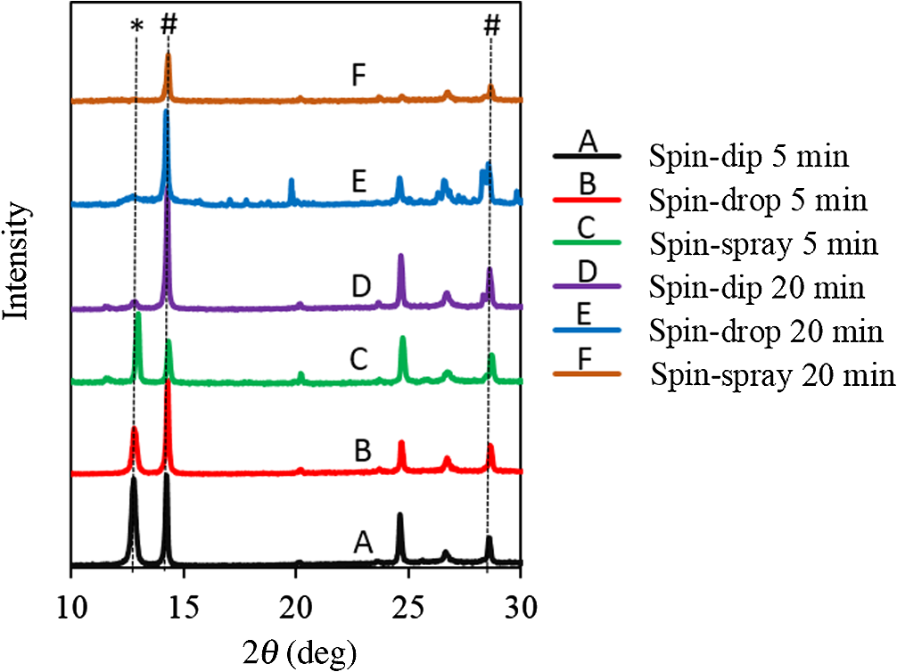 The absorbances of various perovskite films are shown in Fig. 13. In Fig. 13(a), the layer was deposited by spin coating, whereas in Fig. 13(b) spray coating (two spray passes, at the substrate temperature of 50°C) was used to deposit the layer. The MAI solution was deposited by drop, dip, and pulsed-spray coating. It is observed that when spin coating is used to deposit the layer, a higher absorbance is achieved. Although the perovskite films prepared using spray-on films are thicker than the spun-on counterparts (c.f. Fig. 9), Fig. 13 shows that the absorbance of the former is lower than the latter. This may be attributed to the high roughness in spray-on films10 (c.f. Fig. 9). An important result of Fig. 13 is the comparable absorbance of the films made by drop casting, dip coating, and pulsed-spray coating of MAI solution atop . Fig. 13The absorbance spectra of perovskite films fabricated by (a) spin coating and (b) spray coating, as the deposition method for the layer. The MAI solution was deposited using dip, drop, and spray coating. Spray coating of solution was performed based on two spray passes. Spray coating of the MAI solution was performed using pulsed-spray coating, as outlined in the text. concentration = 0.7 M; substrate temperature = 50°C; spray nozzle height = 12 cm; ; and dipping time = 1 h. 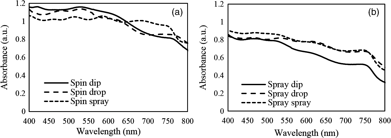 3.4.Device PerformanceIn the last step, PVSCs were fabricated using spin-drop and spray-drop methods, using optimum solution concentration of 0.7 M. Spin coating (reference method) and spray coating (scalable) were used to fabricate the layer. For deposition of the MAI solution, drop casting was chosen owing to its low solution consumption and comparable performance with respect to dip and pulsed-spray coating. For spray coating, two pass spray coatings at a substrate temperature of 50°C, a spray nozzle height of 12 cm, and spray nozzle speed of were used. Figures 14(a) and 14(b) show the SEM cross-sectional images of the representative fabricated devices, without the back contact. The images show that a thin and uniform layer of spun-on with a thickness of less than 100 nm has formed. The perovskite film prepared using spray-drop coating is thicker and less uniform compared to that made using spin-drop coating. The current density–voltage characteristics and a summary of their PV performance parameters are shown in Fig. 14(c) and Table 1, respectively. The inset image in Fig. 14(c) is a picture of an array of spray-drop devices fabricated on one substrate, where the area of each cell is . The highest performance was obtained from a spin-drop cell with the short circuit current of , open circuit voltage () of 0.94 V, FF of 0.634, and PCE of 9.48%, whereas the PCE of the best spray-drop cell is 6.92%, corresponding to of , of 0.88 V, and FF of 0.504. The average PCE obtained from spin-drop cells (8.45%) is also higher than the average value of spray-drop cells (5.95%). The modest device PCE is partly attributed to the exposure of the samples to the high humidity of Shanghai, China, before and after thermal evaporation and during encapsulation. Nevertheless, the results are adequate because the objective of this work is to develop and test facile spray coating and drop casting techniques and to compare the results with those obtained from reference devices fabricated at similar conditions. As mentioned before, the high roughness in the spray-drop perovskite results in a decrease in the absorbance10 and the FF,34 where the latter is due to the increased contact resistance between the nonuniform spray-on layer and its adjacent layers. Also, presumably larger numbers of pinholes in spray-drop perovskite compared to spin-dip device cause a decrease in the shunt resistance creating paths for recombination.37 The of the spin-drop device is higher than that of the spray-drop device. This may be explained as follows. The relatively nonuniform perovskite film made by spray coating may increase the population of pinholes, raising the probability of recombination due to detrimental connection between the electron and hole transporting layers, leading to a decrease in . The smoother and more uniform surface of spin-drop perovskite films results in a decrease in pinholes and voids in the interfaces of the active layer with the upper and lower layers, leading to a lower recombination at the interfaces and a higher .37 Lower current density of the spray-drop device may stem from the lower absorbance of spray-drop perovskite films compared to the spin-drop films (c.f. Fig. 13). In addition to lower absorbance, higher recombination in spray-drop perovskite films compared to spin-drop films may cause a lower . Overall, the difference between the average value of the PCE of the spray-drop and spin-drop devices is about 2.5%, which may be considered acceptable for the spray-drop devices, fabricated using scalable and touch-free coating techniques. It is noted that for commercialization purposes, it is desirable to fabricate all layers using the same scalable method, such as spray coating, but this work focused on the optimization process of the perovskite layer only and the electron- and hole-transporting layers were prepared by conventional spin coating. As to the other layers, as long as the material is solution-processed, it could be deposited using scalable methods, such as spray and blade coating, although fabrication of very thin layers may be challenging. The layer could be readily deposited by spray pyrolysis41 and research is currently being undertaken to substitute flexible spray-on graphene-based42 and nanowire-based43 electrodes for the current (front and back) electrodes, in an attempt to achieve fully solution processed and transparent conducting oxide-free devices. Fig. 14SEM cross-sectional images of planar PVSCs without the back contact, fabricated by (a) spin-drop and (b) spray-drop coating. (c) curves of PVSCs, where the perovskite layer is fabricated by spin-drop and spray-drop coating. The inset image is the picture of the devices made by spray-drop technique. 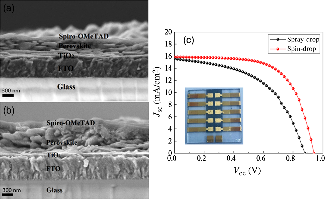 Table 1Photovoltaic performance of the PVSCs fabricated using spin-drop and spray-drop methods.
4.ConclusionThis study focused on optimization of the spray-coating parameters to achieve a fully covered spray-on film as the first step in a sequential deposition of methylammonium lead iodide perovskite layer. Then in the second step, the MAI solution was deposited atop the spray-on and spun-on films by pulsed-spray and also by drop casting as two facile and scalable techniques as well as by conventional dip-coating technique. The optimum concentration of in DMF was found to be to 0.7 M within the experimental conditions of this work. Then, for the spray nozzle used in the work, the spraying conditions were optimized systematically, where the approach can be generalized to other sprays. The optimum number of spray passes varies with the substrate temperature. If the substrate is kept at room temperature, the application of additional spray passes may deteriorate the coverage, whereas at elevated substrate temperatures, where the impinged spray droplets dry rather quickly, application of additional passes improves the coverage. Using multiple spray passes also increases the roughness and thickness of the film, thus reducing the chance of conversion to perovskite, due to higher film thicknesses. As the substrate temperature increases and approaches the boiling point of the solvent, viz. DMF (153°C), the best coverage occurs, even using one spray pass. However, we observed that at elevated substrate temperatures, due to partial sintering and hardening of the crystals, the MAI solution cannot infiltrate the hardened film, thus a full conversion of MAI and precursors to perovskite was not observed. Consequently, for the nozzle and flow rate used in this study, based on a trade-off between coverage, roughness, thickness, and full conversion, the optimum substrate temperature in a sequential deposition is identified to be around 50°C using two spray passes. Subsequently, drop casting and pulsed-spray coating, as well as dip coating, were applied on spun-on films (as the reference samples) and also on spray-on films, to make perovskite films, where the samples fabricated through the three foregoing techniques on spray-on films showed lower absorbance compared to their counterparts fabricated on spun-on films, due to the higher roughness of spray-on films. However, the three techniques used in the second step for deposition of the MAI solution led to the comparable absorbance, both on spun-on and spray-on films. Moreover, it was shown that the consumption of the MAI solution in drop casting is much less than those in dip and spray coating. Finally, devices were fabricated using spin-drop and spray-drop methods, where the best spin-drop device showed higher PCE of 9.48% compared to 6.92% for the best spray-drop device. The results reveal the capability of spray coating and drop casting for the low-cost fabrication of perovskite SCs. AcknowledgmentsResearch funding from the Shanghai Municipal Education Commission in the framework of oriental scholar and funding from the National Natural Science Foundation of China (NSFC) is acknowledged. ReferencesQ. Wang et al.,
“Progress in emerging solution-processed thin film solar cells—Part I: polymer solar cells,”
Renewable Sustainable Energy Rev., 56 347
–361
(2016). http://dx.doi.org/10.1016/j.rser.2015.11.063 Google Scholar
M. Habibi et al.,
“Progress in emerging solution-processed thin film solar cells—Part II: perovskite solar cells,”
Renewable Sustainable Energy Rev., 62 1012
–1031
(2016). http://dx.doi.org/10.1016/j.rser.2016.05.042 Google Scholar
National Renewable Energy Laboratory, “Research cell record efficiency chart,”
(2017) https://www.nrel.gov/pv/assets/images/efficiency-chart.png ( December 2016). Google Scholar
J. Burschka et al.,
“Sequential deposition as a route to high-performance perovskite-sensitized solar cells,”
Nat. Photonics, 499 316
–319
(2013). http://dx.doi.org/10.1038/nature12340 Google Scholar
F. Zabihi, M.-R. Ahmadian-Yazdi and M. Eslamian,
“Fundamental study on the fabrication of inverted planar perovskite solar cells using two-step sequential substrate vibration-assisted spray coating (2S-SVASC),”
Nanoscale Res. Lett., 11 71
(2016). http://dx.doi.org/10.1186/s11671-016-1259-2 Google Scholar
C. Huang et al.,
“Highly efficient perovskite solar cells with precursor composition-dependent morphology,”
Sol. Energy Mater. Sol. Cells, 145 231
–237
(2016). http://dx.doi.org/10.1016/j.solmat.2015.10.032 Google Scholar
C. C. Chen et al.,
“One-step, low-temperature deposited perovskite solar cell utilizing small molecule additive,”
J. Photonics Energy, 5 057405
(2015). http://dx.doi.org/10.1117/1.JPE.5.057405 Google Scholar
M. Liu, M. B. Johnston and H. J. Snaith,
“Efficient planar heterojunction perovskite solar cells by vapour deposition,”
Nature, 501 395
–398
(2013). http://dx.doi.org/10.1038/nature12509 Google Scholar
J. H. Im et al.,
“Growth of cuboids with controlled size for high-efficiency perovskite solar cells,”
Nat. Nanotechnol., 9 927
–932
(2014). http://dx.doi.org/10.1038/nnano.2014.181 Google Scholar
L. Wengeler et al.,
“Comparison of large scale coating techniques for organic and hybrid films in polymer based solar cells,”
Chem. Eng. Process. Process Intensif., 68 38
–44
(2013). http://dx.doi.org/10.1016/j.cep.2012.03.004 Google Scholar
M. Habibi et al.,
“Defect-free large-area () light absorbing perovskite thin films made by spray coating,”
Coatings, 7 42
(2017). http://dx.doi.org/10.3390/coatings7030042 Google Scholar
M. Eslamian and F. Zabihi,
“Ultrasonic substrate vibration-assisted drop casting (SVADC) for the fabrication of photovoltaic solar cell arrays and thin-film devices,”
Nanoscale Res. Lett., 10 462
(2015). http://dx.doi.org/10.1186/s11671-015-1168-9 Google Scholar
M. Habibi, A. Rahimzadeh and M. Eslamian,
“On dewetting of thin films due to crystallization (crystallization dewetting),”
Eur. Phys. J. E., 39 30
(2016). http://dx.doi.org/10.1140/epje/i2016-16030-9 Google Scholar
M. Hçsel, H. F. Dam and F. C. Krebs,
“Development of lab-to-fab production equipment across several length scales for printed energy technologies, including solar cells,”
Energy Technol., 3 293
–304
(2015). http://dx.doi.org/10.1002/ente.201402140 Google Scholar
J. H. Lee, S. Yoshikawa and T. Sagawa,
“Fabrication of efficient organic and hybrid solar cells by fine channel mist spray coating,”
Sol. Energy Mater. Sol. Cells, 127 111
–121
(2014). http://dx.doi.org/10.1016/j.solmat.2014.04.010 Google Scholar
Y. J. Kang et al.,
“Progress towards fully spray-coated semitransparent inverted organic solar cells with a silver nanowire electrode,”
Org. Electron., 15 2173
–2177
(2014). http://dx.doi.org/10.1016/j.orgel.2014.06.016 Google Scholar
J. G. Tait et al.,
“Spray coated high-conductivity PEDOT:PSS transparent electrodes for stretchable and mechanically-robust organic solar cells,”
Sol. Energy Mater. Sol. Cells, 110 98
–106
(2013). http://dx.doi.org/10.1016/j.solmat.2012.09.005 Google Scholar
M. Eslamian and J. Newton,
“Spray-on PEDOT:PSS and P3HT:PCBM thin films for polymer solar cells,”
Coatings, 4 85
–97
(2014). http://dx.doi.org/10.3390/coatings4010085 Google Scholar
Y. Xie, S. Gao and M. Eslamian,
“Fundamental study on the effect of spray parameters on characteristics of P3HT:PCBM active layers made by spray coating,”
Coatings, 5 488
–510
(2015). http://dx.doi.org/10.3390/coatings5030488 Google Scholar
Y. J. Noh et al.,
“Cost-effective ITO-free organic solar cells with silver nanowire-PEDOT:PSS composite electrodes via a one-step spray deposition method,”
Sol. Energy Mater. Sol. Cells, 120 226
–230
(2014). http://dx.doi.org/10.1016/j.solmat.2013.09.007 Google Scholar
A. T. Barrows et al.,
“Efficient planar heterojunction mixed-halide perovskite solar cells deposited via spray-deposition,”
Energy Environ. Sci., 7 2944
–2950
(2014). http://dx.doi.org/10.1039/C4EE01546K Google Scholar
B. A. Nejand et al.,
“New scalable cold-roll pressing for post-treatment of perovskite microstructure in perovskite solar cells,”
J. Phys. Chem. C, 120 2520
–2528
(2016). http://dx.doi.org/10.1021/acs.jpcc.5b11596 Google Scholar
S. Das et al.,
“High-performance flexible perovskite solar cells by using a combination of ultrasonic spray-coating and low thermal budget photonic curing,”
ACS Photonics, 2 680
–686
(2015). http://dx.doi.org/10.1021/acsphotonics.5b00119 Google Scholar
J. G. Tait et al.,
“Rapid composition screening for perovskite photovoltaics via concurrently pumped ultrasonic spray coating,”
J. Mater. Chem. A, 4 3792
–3797
(2016). http://dx.doi.org/10.1039/C6TA00739B Google Scholar
Y. S. Jung et al.,
“Differentially pumped spray deposition as a rapid screening tool for organic and perovskite solar cells,”
Sci. Rep., 6 20357
(2016). http://dx.doi.org/10.1038/srep20357 Google Scholar
P. S. Chandrasekhar et al.,
“Fabrication of perovskite films using an electrostatic assisted spray technique: the effect of the electric field on morphology, crystallinity and solar cell performance,”
Nanoscale, 8 6792
–6800
(2016). http://dx.doi.org/10.1039/C5NR08350H Google Scholar
Z. Liang, X. Xu and J. Wang,
“A facile spray deposition route for uniform perovskite solar cells processed in air international photonics and optoelectronics,”
in Int. Photonics and OptoElectronics Conf.,
(2015). Google Scholar
F. Li et al.,
“A facile spray-assisted fabrication of homogenous flat films for high performance mesostructure perovskite solar cells,”
Mater. Lett., 157 38
–41
(2015). http://dx.doi.org/10.1016/j.matlet.2015.05.106 Google Scholar
Z. Liang et al.,
“A large grain size perovskite thin film with a dense structure for planar heterojunction solar cells via spray deposition under ambient conditions,”
RSC Adv., 5 60562
(2015). http://dx.doi.org/10.1039/C5RA09110A Google Scholar
N. Mohammadian et al.,
“A two-step spin-spray deposition processing route for production of halide perovskite solar cell,”
Thin Solid Films, 616 754
–759
(2016). http://dx.doi.org/10.1016/j.tsf.2016.09.039 Google Scholar
A. K. Chilvery et al.,
“Efficient planar perovskite solar cell by spray and brush solution-processing methods,”
J. Photonics Energy, 5 053093
(2015). http://dx.doi.org/10.1117/1.JPE.5.053093 Google Scholar
Z. Bi et al.,
“Fast preparation of uniform large grain size perovskite thin film in air condition via spray deposition method for high efficient planar solar cells,”
Sol. Energy Mater. Sol. Cells, 162 13
–20
(2017). http://dx.doi.org/10.1016/j.solmat.2016.12.032 Google Scholar
H. Huang et al.,
“Two-step ultrasonic spray deposition of for efficient and large-area perovskite solar cell,”
Nano Energy, 27 352
–358
(2016). http://dx.doi.org/10.1016/j.nanoen.2016.07.026 Google Scholar
C. Girotto et al.,
“High-performance organic solar cells with spray-coated hole-transport and active layers,”
Adv. Funct. Mater., 21 64
–72
(2011). http://dx.doi.org/10.1002/adfm.201001562 Google Scholar
G. Susanna et al.,
“Airbrush spray-coating of polymer bulk-heterojunction solar cells,”
Sol. Energy Mater. Sol. Cells, 95 1775
–1778
(2011). http://dx.doi.org/10.1016/j.solmat.2011.01.047 Google Scholar
S. Y. Park et al.,
“Spray-coated organic solar cells with large-area of ,”
Sol. Energy Mater. Sol. Cells, 95 852
–855
(2011). http://dx.doi.org/10.1016/j.solmat.2010.10.033 Google Scholar
M. Ramesh et al.,
“Using an airbrush pen for layer-by-layer growth of continuous perovskite thin films for hybrid solar cells,”
Appl. Mater. Interfaces, 7 2359
–2366
(2015). http://dx.doi.org/10.1021/am506886d Google Scholar
C. Sun et al.,
“Solvent-assisted growth of organic–inorganic hybrid perovskites with enhanced photovoltaic performances,”
Sol. Energy Mater. Sol. Cells, 143 360
–368
(2015). http://dx.doi.org/10.1016/j.solmat.2015.07.021 Google Scholar
M. Eslamian,
“A mathematical model for the design and fabrication of polymer solar cells by spray coating,”
Drying Technol., 31 405
–413
(2013). http://dx.doi.org/10.1080/07373937.2012.737397 Google Scholar
M. Eslamian,
“Spray-on thin film PV solar cells: advances, potentials and challenges,”
Coatings, 4 60
–84
(2014). http://dx.doi.org/10.3390/coatings4010060 Google Scholar
T. Supasai et al.,
“Compact nanostructured deposited by aerosol spray pyrolysis for the hole-blocking layer in a perovskite solar cell,”
Solar Energy, 136 515
–524
(2016). http://dx.doi.org/10.1016/j.solener.2016.07.035 Google Scholar
F. Zabihi and M. Eslamian,
“Low-cost transparent graphene electrodes made by ultrasonic substrate vibration-assisted spray coating (SVASC) for thin film devices,”
Graphene Technol., 1
–11
(2017). http://dx.doi.org/10.1007/s41127-017-0003-8 Google Scholar
K. Yang et al.,
“All-solution processed semi-transparent perovskite solar cells with silver nanowires electrode,”
Nanotechnology, 27 095202
(2016). http://dx.doi.org/10.1088/0957-4484/27/9/095202 Google Scholar
BiographyMehran Habibi is a PhD student at the University of Michigan-Shanghai Jiao Tong University Joint Institute and focuses on the fabrication of thin film perovskite solar cells and transistors using scalable methods, such as spray and blade coating. Mohammad-Reza Ahmadian-Yazdi is an MS degree student at the University of Michigan-Shanghai Jiao Tong University Joint Institute and focuses on the fabrication of perovskite solar cells using ultrasonic vibration-assisted deposition of the perovskite layer for the development of post annealing-free devices. Morteza Eslamian is an associate professor at the University of Michigan-Shanghai Jiao Tong University Joint Institute and cross appointed at the State Key Lab for Composite Materials, School of Materials Science and Engineering, Shanghai Jiao Tong University. He focuses on thermal fluid sciences and their applications in materials synthesis, such as thin film photovoltaics. |