|
|
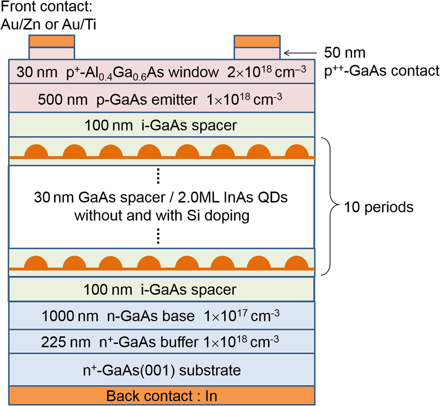
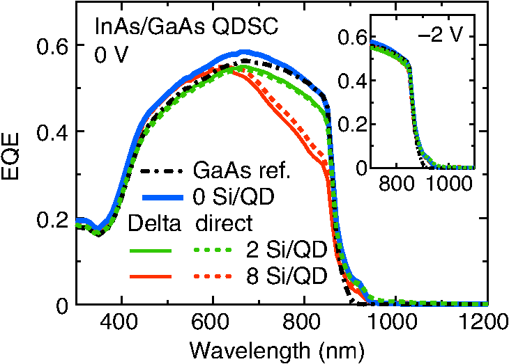
1.IntroductionA high-density array of quantum dots (QDs) incorporated in the active region of a p-i-n single-junction solar cell (SC) has attracted significant interest as a potential intermediate band solar cell (IBSC), which can harvest the subbandgap infrared solar photons to generate an additive photocurrent to that corresponding to the valence-to-conduction band (VB–CB) optical absorption, through two-step photon absorption via intermediate band (IB).1 If such a nanostructured SC was realized, the theoretical conversion efficiency of IBSC has been shown to exceed the Shockley–Queisser limit of conventional single-junction SC,2 and the maximum efficiency for an optimized SC incorporating one IB is shown to be under one sun and 63% under full solar concentration.1,3 In QD-IBSCs, QDs are required to be homogeneous and small in size and should also be regularly and tightly placed. This structural configuration then leads to formation of an IB that is well separated in energy from the higher energy states.4 Second, the IB states need to be partially filled or ideally be half-filled with electrons to ensure an efficient pumping of electrons, thereby providing both the empty states to receive electrons being photoexcited from the valence band (VB) and filled states to promote electrons from IB to the conduction band (CB) via absorption of second subbandgap photons.1,3 Thus, the proposed implementation of QD-IBSCs must accompany an efficient two-step carrier generation via IB states, however, it has been a challenge to notably demonstrate this operation principle particularly at room temperature,5 which is owed to a relatively small optical generation rate from the QD-IB states to CB. The rate of thermal escape of electrons from IB to CB continuum as well as recombination from CB to IB transitions (reverse process) increases significantly with increasing temperature,6–8 and these processes inevitably lead to a drop in the open-circuit voltage and eventually outweigh the current gained by QD absorption. The present development of QD-IBSCs is thus undergoing three stages. The first is to develop technology to fabricate high-density QDs array with low interface defect density and longer carrier lifetimes in an optimized QD/host material bandgap system.1 The fabrication of QDs array is most commonly achieved by taking advantage of spontaneous self-assembly of coherent three-dimensional islands in lattice-mismatched epitaxy, well known as Stranski–Krastanov (S–K) growth. The second is to minimize thermal escape of carriers out of QDs at room temperature. The QD-IBSCs, where the matrix material is a wide-bandgap semiconductor, have been studied to demonstrate a larger band offset between the IB and the host material.6,9–11 The third stage is to realize partially filled or ideally half-filled IB states to maximize the photocurrent generation by two-step photon absorption. Martí et al.9 and the works that follow12–19 have employed the modulation-doping technique to fabricate QD-IBSCs, in which each GaAs barrier/spacer layer was delta ()-doped with Si with a sheet density equal to or larger than the InAs QDs areal density. On the other hand, Strandberg and Reenaas20 have performed a simulation and have shown that under radiative limit, IB must be partially filled by means of doping within a reasonable optical length to achieve high efficiency if QD-IBSCs were to be operated under one sun condition. It would, however, become possible to sustain a reasonable population of photogenerated electrons even in a nondoped QD-IBSC under concentrated sunlight, typically 100 to 1000 suns. Yoshida et al.21,22 also reported similar calculated results based on a self-consistent device simulation method. Although the theoretical analysis of IBSCs commonly adopts a detailed balanced model,2 Sullivan et al.23 have recently shown that the optical and nonradiative electrical trapping cross sections of impurities in the IB region determine the performance of IBSCs in the case of the nonradiative recombination lifetimes dominating over radiative lifetimes. Recently, Si has been commonly studied as an -type dopant in InAs/GaAs QD structures by two doping methods: -doping9,12–19 and direct doping.5,24–26 In -doping, Si is doped into GaAs barrier/spacer layers among InAs QD layers. In direct doping, Si is supplied directly into InAs QDs during the assembling stage of S–K growth. It has been demonstrated that Si doping improves photoluminescence (PL) intensity from QDs and increases the thermal activation energy of QD states for both the -doped and direct-doped QDs. For SC application, an enhancement of short-circuit current density () in -doped quantum dots solar cells (QDSCs)5,15,19 and recovery of in direct-doped QDSCs have been observed.16,26,27 The purpose of this work is to investigate the effect of Si-doping density, Si-doping methods by both the modulation/-doping, and the direct doping, and the sunlight concentration on the performance of InAs/GaAs QDSCs. Particular attention is paid to study the effect of changing the filling ratio of IB states by the Si doping and the photofilling by sunlight concentration on recovery of from the viewpoint of understanding and demonstrating the control of filling ratio of IB in SC operation. 2.Simulated Performance of Intermediate Band Solar Cells with Doping and Under ConcentrationA self-consistent drift-diffusion simulation21,22 was performed to clarify the effect of doping in the QD-IB region and the effect of sunlight concentration on the SC characteristics. Here, the optical generation () and recombination () rates between VB–IB and IB–CB are assumed to be locally balanced, i.e., It is noted that and are roughly proportional to and , respectively, where is the filling or occupancy ratio of IB states as shown in Fig. 1. Thus, the subbandgap optical absorptions via IB depend critically on the filling ratio of IB and the potential profile, where the charge density at each position is given by where is the hole density in VB, is the electron density in CB, is the electron density in IB, and are the ionized donor and acceptor densities, and is the elementary charge, respectively.Fig. 1Schematic drawing of IBSC structure and energy band diagram considered for device simulation. The IB region is assumed to be thick and either nondoped or doped (-doping) such that the filling ratio in IB can be varied. Possible photoabsorption and recombination processes are shown in the energy diagram. 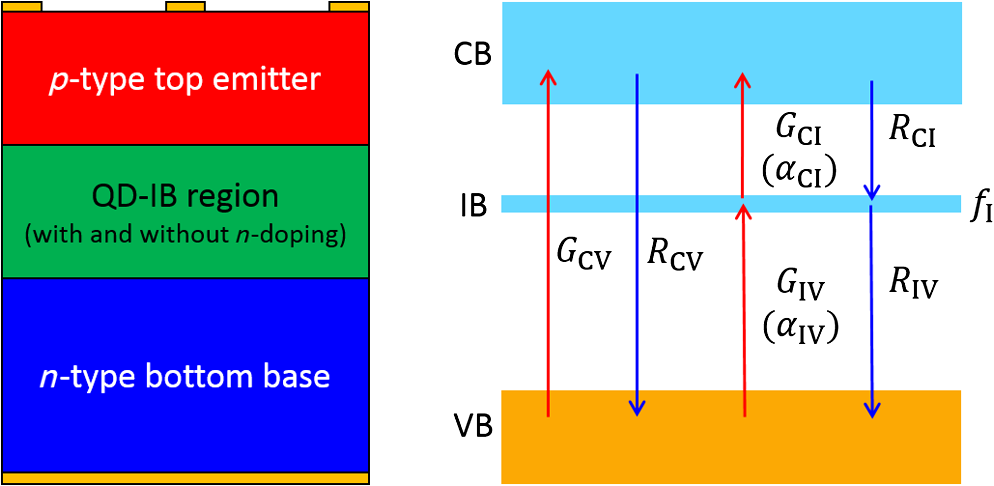 For the simulation, a solar spectrum from a blackbody at 5800 K was used. For the SCs, ideal Ohmic contacts were assumed for the majority carrier current flow as well as zero surface recombination velocity for the minority carriers. The zero surface recombination velocity refers to an ideal passivation of the surface and equivalently a lossless window layer. The dark current can then be determined by the total amount of recombination processes inside the cell. Two cases of IBSCs as schematically shown in Fig. 1 were modeled; IB region of thickness was (1) nondoped, written as , and (2) -doped for which the filling ratio of IB states with electrons or 0.5. We believe that a -thick IB region is almost an optimum thickness from the viewpoint of carrier lifetime and diffusion length. The material parameters used were from the database available for GaAs at 300 K except for the values of absorption coefficients as reported previously.21,22 The energy gaps of CB–VB and IB–VB were taken as 1.43 and 0.95 eV, respectively, and the simulation assumes an equivalent QD in-plane density of , which is about the same as QDs fabricated experimentally. To understand the intrinsic effects of impurity doping in IB and sunlight concentration, a simple case for the absorption coefficients was employed, in which the absorption coefficients for VB to CB () and for VB to IB () were taken to be , and the ratio of was then varied in the range of 0.01 to 1.0 while was fixed. Furthermore, nonradiative recombination processes were not considered and the overlap of absorption coefficients among various transitions was also assumed ideal as zero.20–22 The simulated as given by normalized by , , and cell efficiency are plotted as a function of sunlight concentration ratio for IBSCs and for single-junction GaAs reference SC as shown in Figs. 2(a) through 2(c), respectively. As shown in Fig. 2(a), in the case of , where the absorption coefficients are large and equal, in IBSC (dashed line) with nondoped IB () shows a strong nonlinear dependence on compared with IBSC with doped IB. For the half-filled case (), (solid line) shows a marginal increase with increasing . Further, in nondoped IBSC approaches that of doped IBSC as becomes larger than 1000 suns as a result of the photofilling effect. However, in the case of , shows only a small increase with increasing regardless of whether IB is nondoped or doped, though the half-filled IBSC () still produces the highest (solid line). Fig. 2(a) , (b) , and (c) cell efficiency calculated for IBSCs with nondoped and doped (-doping) IB region as a function of sunlight concentration ratio , respectively. The is normalized by the concentration ratio . 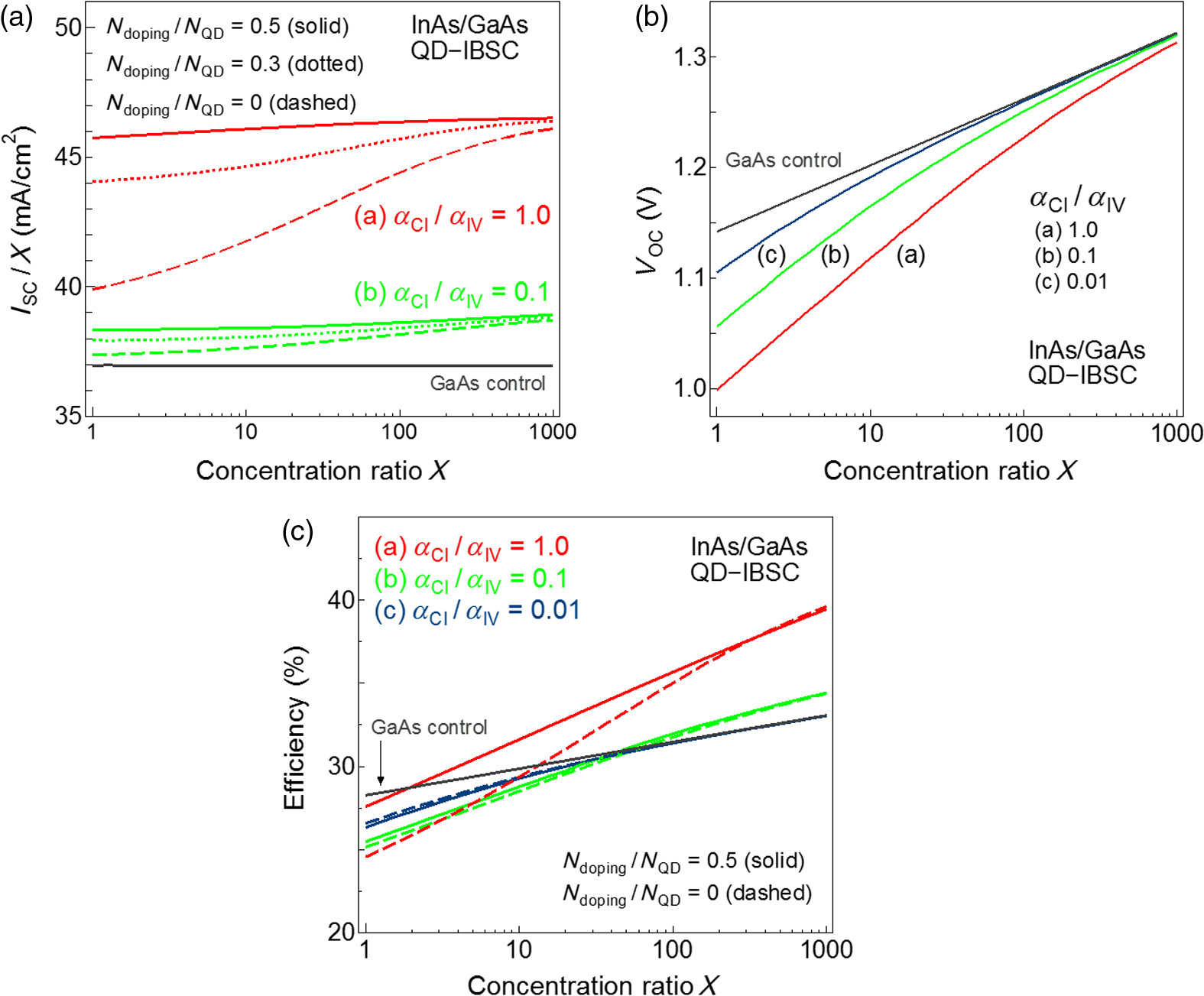 On the other hand, is strongly dependent on in both IBSCs and no noticeable difference in is observed for nondoped or doped cases as shown in Fig. 2(b). This is because the radiative recombination process between CB and VB dominates in low bias range under high compared with recombination rates via IB. Thus, the operation of IBSCs becomes similar to that of GaAs single-junction SC under a high sunlight concentration and results in a value of which is similar to that of GaAs single-junction SC. One further point to be noted is that IBSC with a small absorption ratio of shows a higher than for and an even higher value compared with the case of , although a higher ratio is more desirable from the view point of producing a higher as determined from Fig. 2(a). This is the case because of the reciprocity nature of absorption and recombination processes. A higher absorption coefficient results in a higher optical generation rate as of Fig. 1, but at the same time, also increases. Therefore, for a given value of filling ratio of IB, approximated by , becomes smaller for . However, of close to unity still needs to be realized to achieve the cell efficiency toward 40% as shown in Fig. 2(c). 3.Experiments and ResultsWe have fabricated three types of InAs/GaAs QDSCs with different Si-doping concentrations by either -doping or direct-doping method. Though the characterization on the filling factor of QDs is important, the analysis is complicated by the fact that the filling of QDs with electrons is unlikely to be uniform. It is possible that larger QDs are filled with more electrons than smaller QDs and that some are trapped to passivate the defects. To this end, we express the average number of doped Si, per QD as, Si/QD. A schematic of QDSC structure fabricated is shown in Fig. 3, and a 10-layer multistacked InAs/GaAs QD structure was inserted in the -region of a GaAs p-i-n SC. Although the experimental IB region in this study is limited to thickness with 10 stacked QD layers, we believe that the key features observed in the characterization can still be well addressed based on the simulation results as of Fig. 2, which assumes thick IB region. All samples were grown by molecular beam epitaxy.28 Each QD pair consisted of a 2.0 monolayer InAs QD layer and a 30-nm GaAs spacer/barrier layer. The growth temperature was 580°C except for the -GaAs spacer layer and InAs/GaAs QD layer, for which the temperature was lowered to 480°C. The growth rates were for GaAs and layers and for InAs QD layers, respectively. The Si doping was varied among 0, 2, and 8 Si/QD. The in-plane density of InAs QDs was acquired from the atomic force microscope (AFM) image of a separately grown sample without capping the topmost QD surface of 10-period InAs/GaAs QD sample. The average size of the QDs was in diameter and in height, and the in-plane QD density was . The variations in size and in-plane density of QDs for all samples with different Si-doping concentrations and doping method were practically within the experimental variation and hence considered the same. For the current–voltage () measurements at one sun and external quantum efficiency (EQE) characterization, Au/Zn ohmic contact was used as the top electrode, and In was used as the bottom contact. Each device was cleaved to an area of . For high sunlight intensity measurements, Au/Ti ohmic contact was deposited using an electron beam evaporator as the top contact and In for the bottom contact. Here, each concentrator SC was mesa etched to an area of . In the three types of InAs/GaAs QDSCs (0, 2, and 8 Si/QD), Si was doped by either -doping or direct doping.28 In -doping, Si was doped into the GaAs spacer layer at a position of 11.0 to 11.8 nm above the QD layer, whereas in direct doping, Si was supplied during the self-assembling step of QD growth.5,24 3.1.Effect of Si Doping on InAs/GaAs Quantum Dots Solar Cell CharacteristicsThe curves were measured under one sun illumination with air mass (AM) 1.5 spectrum at room temperature. As shown in Fig. 4, a recovery of is clearly observed for QDSCs with Si doping. The gradually recovers with increasing Si doping in both QDSCs grown with -doping and direct doping and increases by and 80 mV for Si-doped QDSCs with 2 and 8 Si/QD, respectively, as compared with nondoped QDSC (0 Si/QD). Based on the simulation as of Fig. 2(b), the filling ratio of IB, , and hence the optical generation rate by -doping fundamentally affect . Recently, the recovery of in -doped QDSCs has been attributed to reduce nonradiative recombination via QD states.16,26,27 Thus, we believe that -doping plays an important role in controlling the optical processes via QD states and also in reducing the nonradiative processes. Fig. 4characteristics of InAs/GaAs QDSCs measured under one sun illumination with AM 1.5 spectrum at room temperature. The doping of QDs was varied as 0, 2, and 8 Si/QD both by -doping and direct doping methods. 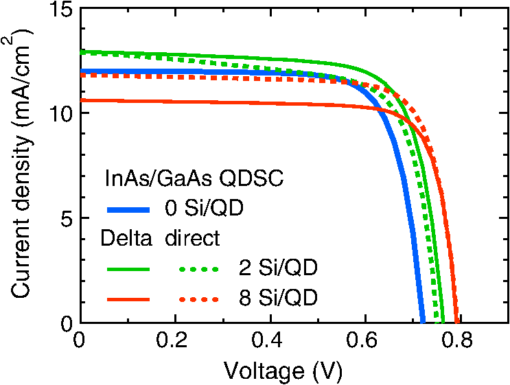 On the other hand, the shows a more complex behavior in which increases for 2 Si/QDSCs but becomes lower for 8 Si/QDSCs. From the EQE data, as shown in Fig. 5, the EQE response in the wavelength range of 700 to 900 nm is degraded especially for 8 Si/QDSCs compared with nondoped SCs. This reduction in EQE is responsible for smaller . However, we believe that this does not originate from the crystal quality of QDs and interfaces because the EQE is fully recovered when measured under a reverse bias of as can be clearly seen from the inset of Fig. 5. Apart from the partial filling of QD states as well as defect reduction achieved by Si doping, Sellers et al.17 have shown that electron doping produces negatively charged QDs that could exert a repulsive Coulomb force on the free electrons in CB, thereby reducing the probability of electron capture into QDs. Hence, a higher collection efficiency of photocarriers is expected. This model could also qualitatively explain our results of an increased obtained for 2 Si/QDSCs compared with 0 Si/QDSCs. A heavier doping as in the case of 8 Si/QDSCs then decreases the photocarrier collection due to an increased rate of electron capture into QDs for which the energy band of the QD region is more flattened by the heavier doping.18 A more comprehensive analysis is necessary to fully understand the effect of doping on carrier transport and collection processes in QDSCs. 3.2.Effect of Sunlight Concentration on InAs/GaAs Quantum Dots Solar Cell CharacteristicsThe measurements were also performed under concentrated sunlight illumination. The light emitted from a Xe flash lamp was filtered using an AM 1.5 filter. To minimize the effect of cell temperature variation, each scan was completed within 2-ms light pulse duration, and the cell temperature was kept at 298 K using a Peltier-controlled sample stage. Figures 6(a) and 6(b) plot the dependence of for -doped and direct-doped QDSCs, respectively, as a function of the sunlight concentration ratio, . For reference, the measured plot for a GaAs SC is also shown.29 Fig. 6Measured for (a) -doped and (b) direct-doped QDSCs as a function of concentration ratio . The Si doping of QDs was varied as 0, 2, and 8 Si/QD. 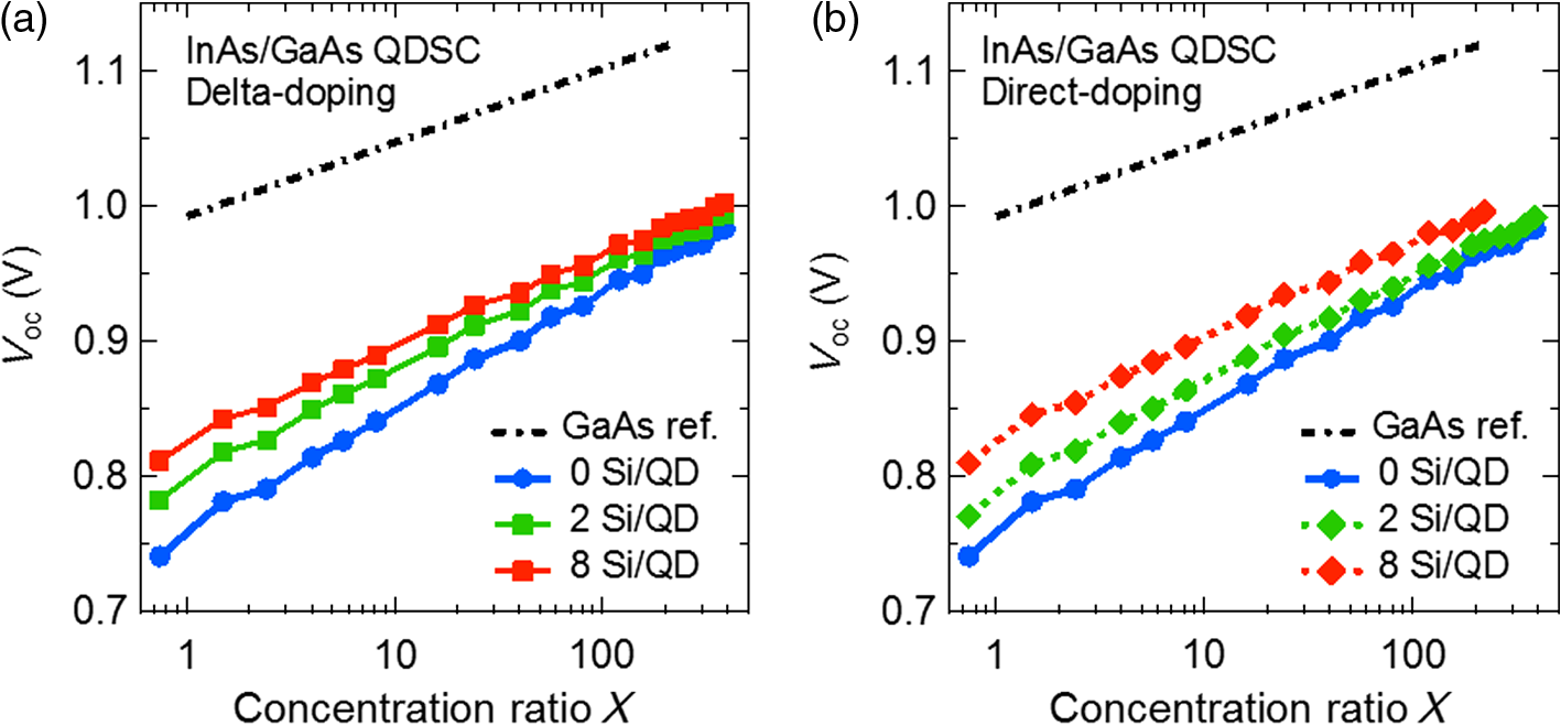 In the low sunlight concentration range, is expected to increase with increasing Si doping, as shown in Fig. 4. A enhancement with logarithmic is attributed to an increase in the ratio of photocurrent to dark current.30 The for heavily doped QDSCs (8 Si/QD) are larger than those with lower doped QDSCs (0 and 2 Si/QD) in all ranges of sunlight concentration ratio up to 400 suns. On the other hand, larger amounts of recovery are obtained for the lower Si-doped QDSCs as compared with 8 Si/QDSCs. The general trend of obtained for different Si-doping densities agrees with the simulation result as of Fig. 2(b) for which curves are plotted for different absorption or recombination rates. An increase of in -doped QDSCs means a decrease of recombination via QD states. Furthermore, under high-concentrated sunlight illumination, in addition to the predoping effect, the QD states become additionally filled by excessively generated photocarriers, i.e., photofilling effect. In this situation, the impact of the photofilling effect becomes dominant, and the effect of predoping by Si becomes small in relative comparison. As a result, for nondoped (0 Si/QD) SC approaches that for the doped QDSCs under high sunlight concentration ratios. Therefore, the results shown in Fig. 6 indicate that both the prefilling of QDs by Si doping and the photofilling by sunlight concentration are effective in obtaining a higher recovery rate and efficiency. Finally, we observe that these features do not seem to depend on the method of Si doping by -doping or direct doping. 4.SummaryIn this work, we have systematically investigated the effect of doping on InAs/GaAs QDs by both simulation and experiments. The prefilling by Si doping of InAs/GaAs QDs was performed using two methods: -doping and direct doping. First, we did not observe clear differences in the Si-doping method between the direct doping and -doping, at least through the characterization of QDs by AFM, PL, and SC characteristics studied in this work. Further, the analysis is complicated by the fact that the filling of QDs with electrons is unlikely to be uniform. It is expected that larger QDs are filled with more electrons than smaller QDs and that some are trapped to passivate the defects. Second, an increase in with increasing Si-doping density was observed, which in turn suggested a decrease of recombination via QD states by Si doping. Moreover, under high-concentrated sunlight illumination, QD states were additionally filled by excessively generated photocarriers or by the photofilling effect. In this situation, the impact of the photofilling effect became dominant, and the effect of predoping by Si became small in relative comparison. The observed features did not seem to depend on the method of Si doping using -doping or direct doping in our studies. On the other hand, the showed a more complex behavior because the Si doping would affect the potential profile and hence carrier collection in SCs. A more comprehensive analysis is necessary to fully understand the effect of doping on carrier transport and collection processes in QDSCs. The control of filling ratio of QD-IB states is important to ensure an efficient pumping of electrons, thereby providing both the empty states to receive electrons being photoexcited from VB and filled states to promote electrons from IB to CB via absorption of second subbandgap photons. To address this issue, we have studied the effect of both the predoping by Si doping and the photofilling by sunlight concentration on the SC characteristics, although further optimization is needed to enhance the two-step photon absorption via the QD states and hence increase the current for higher efficiency operation. AcknowledgmentsThis work has received support from the New Energy and Industrial Technology Development Organization (NEDO) and Ministry of Economy, Trade and Industry (METI), and Japan Society for the Promotion of Science (JSPS) KAKENHI #26246017. One of the authors (S.N.) also thanks support by the JSPS through Program for Leading Graduate Schools (MERIT). ReferencesA. Luque and A. Martí,
“Increasing the efficiency of ideal solar cells by photon induced transitions at intermediate levels,”
Phys. Rev. Lett., 78 5014
–5017
(1997). http://dx.doi.org/10.1103/PhysRevLett.78.5014 PRLTAO 0031-9007 Google Scholar
W. Shockley and H. J. Queisser,
“Detailed balance limit of efficiency of p-n junction solar cells,”
J. Appl. Phys., 32 510
–519
(1961). http://dx.doi.org/10.1063/1.1736034 JAPIAU 0021-8979 Google Scholar
Y. Okada et al.,
“Intermediate band solar cells: recent progress and future directions,”
Appl. Phys. Rev., 2 021302
(2015). http://dx.doi.org/10.1063/1.4916561 Google Scholar
S. Tomić, T. S. Jones and N. M. Harrison,
“Absorption characteristics of a quantum dot array induced intermediate band: implications for solar cell design,”
Appl. Phys. Lett., 93 263105
(2008). http://dx.doi.org/10.1063/1.3058716 APPLAB 0003-6951 Google Scholar
Y. Okada et al.,
“Increase in photocurrent by optical transitions via intermediate quantum states in direct-doped InAs/GaNAs strain-compensated quantum dot solar cell,”
J. Appl. Phys., 109 024301
(2011). http://dx.doi.org/10.1063/1.3533423 JAPIAU 0021-8979 Google Scholar
R. Tamaki et al.,
“Spectrally resolved intraband transitions on two-step photon absorption in InGaAs/GaAs quantum dot solar cell,”
Appl. Phys. Lett., 105 073118
(2014). http://dx.doi.org/10.1063/1.4893879 APPLAB 0003-6951 Google Scholar
T. Kada et al.,
“Two-step photon absorption in InAs/GaAs quantum-dot superlattice solar cells,”
Phys. Rev. B, 91 201303
(2015). http://dx.doi.org/10.1103/PhysRevB.91.201303 Google Scholar
A. Datas et al.,
“Intermediate band solar cell with extreme broadband spectrum quantum efficiency,”
Phys. Rev. Lett., 114 157701
(2015). http://dx.doi.org/10.1103/PhysRevLett.114.157701 PRLTAO 0031-9007 Google Scholar
A. Martí, L. Cuadra and A. Luque,
“Partial filling of a quantum dot intermediate band for solar cells,”
IEEE Trans. Electron. Dev., 48 2394
–2399
(2001). http://dx.doi.org/10.1109/16.954482 IETDAI 0018-9383 Google Scholar
T. Sugaya et al.,
“InGaP-based InGaAs quantum dot solar cells with GaAs spacer layer fabricated using solid-source molecular beam epitaxy,”
Appl. Phys. Lett., 101 133110
(2012). http://dx.doi.org/10.1063/1.4755757 APPLAB 0003-6951 Google Scholar
I. Ramiro et al.,
“Wide-bandgap InAs/InGaP quantum-dot intermediate band solar cells,”
IEEE J. Photovoltaics, 5 840
–845
(2015). http://dx.doi.org/10.1109/JPHOTOV.2015.2402439 IJPEG8 2156-3381 Google Scholar
A. Luque et al.,
“Operation of the intermediate band solar cell under nonideal space charge region conditions and half filling of the intermediate band,”
J. Appl. Phys., 99 094503
(2006). http://dx.doi.org/10.1063/1.2193063 JAPIAU 0021-8979 Google Scholar
Y. D. Jang et al.,
“Enhanced room-temperature quantum-dot effects in modulation-doped InAs/GaAs quantum dots,”
Appl. Phys. Lett., 95 171902
(2009). http://dx.doi.org/10.1063/1.3255017 APPLAB 0003-6951 Google Scholar
K. Wang et al.,
“Si delta doping inside InAs/GaAs quantum dots with different doping densities,”
J. Vac. Sci. Technol. B, 30 041808
(2012). http://dx.doi.org/10.1116/1.4732462 JVTBD9 1071-1023 Google Scholar
K. A. Sablon et al.,
“Strong enhancement of solar cell efficiency due to quantum dots with built-in charge,”
Nano Lett., 11 2311
–2317
(2011). http://dx.doi.org/10.1021/nl200543v NALEFD 1530-6984 Google Scholar
X. Yang et al.,
“Improved efficiency of InAs/GaAs quantum dots solar cells by Si-doping,”
Sol. Energy Mater. Sol. Cells, 113 144
–147
(2013). http://dx.doi.org/10.1016/j.solmat.2013.02.005 SEMCEQ 0927-0248 Google Scholar
D. G. Sellers et al.,
“Analyzing carrier escape mechanisms in InAs/GaAs quantum dot p-i-n junction photovoltaic cells,”
Appl. Phys. Lett., 104 223903
(2014). http://dx.doi.org/10.1063/1.4881181 APPLAB 0003-6951 Google Scholar
S. J. Polly et al.,
“Delta-doping effects on quantum-dot solar cells,”
IEEE J. Photovoltaics, 4 1079
–1085
(2014). http://dx.doi.org/10.1109/JPHOTOV.2014.2316677 IJPEG8 2156-3381 Google Scholar
T. Li et al.,
“Enhanced carrier collection efficiency and reduced quantum state absorption by electron doping in self-assembled quantum dot solar cells,”
Appl. Phys. Lett., 106 053902
(2015). http://dx.doi.org/10.1063/1.4907348 APPLAB 0003-6951 Google Scholar
R. Strandberg and T. W. Reenaas,
“Drift-diffusion model for intermediate band solar cells including photofilling effects,”
Prog. Photovoltaics Res. Appl., 19 21
–32
(2011). http://dx.doi.org/10.1002/pip.v19.1 PPHOED 1062-7995 Google Scholar
K. Yoshida, Y. Okada and N. Sano,
“Self-consistent simulation of intermediate band solar cells: effect of occupation rates on device characteristics,”
Appl. Phys. Lett., 97 133503
(2010). http://dx.doi.org/10.1063/1.3488815 APPLAB 0003-6951 Google Scholar
K. Yoshida, Y. Okada and N. Sano,
“Device simulation of intermediate band solar cells: effects of doping and concentration,”
J. Appl. Phys., 112 084510
(2012). http://dx.doi.org/10.1063/1.4759134 JAPIAU 0021-8979 Google Scholar
J. T. Sullivan et al.,
“Targeted search for effective intermediate band solar cell materials,”
IEEE J. Photovoltaics, 5 212
–218
(2015). http://dx.doi.org/10.1109/JPHOTOV.2014.2363560 IJPEG8 2156-3381 Google Scholar
T. Inoue et al.,
“Impurity doping in self-assembled InAs/GaAs quantum dots by selection of growth steps,”
J. Appl. Phys., 108 063524
(2010). http://dx.doi.org/10.1063/1.3483252 JAPIAU 0021-8979 Google Scholar
T. Kita, R. Hasegawa and T. Inoue,
“Suppression of nonradiative recombination process in directly Si-doped InAs/GaAs quantum dots,”
J. Appl. Phys., 110 103511
(2011). http://dx.doi.org/10.1063/1.3660794 JAPIAU 0021-8979 Google Scholar
P. Lam et al.,
“Voltage recovery in charged InAs/GaAs quantum dot solar cells,”
Nano Energy, 6 159
–166
(2014). http://dx.doi.org/10.1016/j.nanoen.2014.03.016 Google Scholar
F. Cappelluti, M. Gioannini and A. Khalili,
“Impact of doping on InAs/GaAs quantum-dot solar cells: a numerical study on photovoltaic and photoluminescence behavior,”
Sol. Energy Mater. Sol. Cells, 157 209
–220
(2016). http://dx.doi.org/10.1016/j.solmat.2016.05.049 SEMCEQ 0927-0248 Google Scholar
S. Naitoh et al.,
“Effect of Si doping on performance of quantum dot solar cells,”
in 31st European Photovoltaic Solar Energy Conf. and Exhibition,
(2015). Google Scholar
K. Watanabe et al.,
“Open-circuit-voltage enhancement of the III-V super-lattice solar cells under optical concentration,”
in AIP Conf. Proc.,
40
–43
(2012). http://dx.doi.org/10.1063/1.4753829 Google Scholar
S. A. Blokhin et al.,
“AlGaAs/GaAs photovoltaic cells with an array of InGaAs QDs,”
Semiconductors, 43 514
–518
(2009). http://dx.doi.org/10.1134/S1063782609040204 SMICES 1063-7826 Google Scholar
|